Unit-1
Small Signal Amplifiers
Common Base Configuration
- The notation and symbols of pnp and npn transistors are given below:
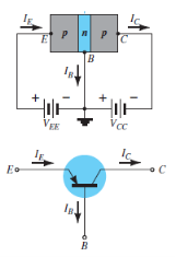 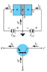 |
Fig. 1: PNP CB and NPN CB (Ref. 2)
- Here the base is common to both the input and output sides of the configuration.
- The flow of holes will govern the direction of current.
- Hence, Ic = Ib + Ie
Where Ic, Ib, Ie are the collector, base and emitter currents respectively.
- The graphical symbol of the PNP common base configuration is
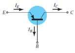 |
Fig. 2: PNP common base (Ref. 2)
- The arrow in the above symbol shows the direction of emitter current in the device.
- Now, to study the behaviour of the device we require two characteristics:
Input Characteristic Curve
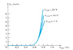 |
Fig.3: Input Characteristic Curve (Ref. 2)
- It is the relation between the input current IE to the input voltage VBE for various levels of output voltage VCB.
- It is also known as driving point characteristics.
Output Characteristic Curve
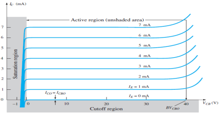 |
Fig.4: Output Characteristic Curve (Ref. 2)
- It is the relation between the output current IC to the output voltage VCB for various levels of input current IE.
- It is also known as collector set of characteristics.
- It has three basic regions:
- Active Region
- Here, base-emitter junction is forward biased and collector-base junction is reverse biased.
- As input current IE increases above zero, output current IC increases to a magnitude equal to IE as determined by the basic transistor current relationship.
- So the first approximation determined by the curve is
IC ≈ IE
2. Cut-off Region
- It is defined as the region where the collector current IC is equal to 0A.
- Here, the base-emitter junction and the collector-base junction both are in reverse bias.
3. Saturation Region
- It is the region that lies towards the left of VCB = 0V.
- Here, the base-emitter junction and the collector-base junction both are in forward bias.
Common Emitter Configuration
- The notation and symbols of npn and pnp transistors are given below:
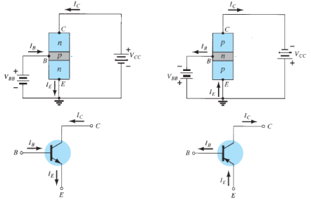 |
Fig. 5: NPN CE and PNP CE (Ref. 2)
- In the above figure all the currents are shown in their actual conventional directions.
- The current relation developed earlier is still applicable,
IE = IB + IC
Where IE , IB , IC are the collector, base and emitter currents respectively.
- The graphical symbol of the PNP common emitter configuration is
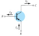 |
Fig.6: PNP common emitter (Ref. 2)
- Now, to study the behaviour of the device we require two characteristics:
Input Characteristic Curve
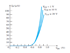 |
Fig.7: Input Characteristic Curve (Ref. 2)
- It is the graph between the input current IB to the input voltage VBE for a range of values of output voltage VCE.
- Note that the magnitude IB of is in micro amperes and that of IC is in milli amperes.
Output Characteristic Curve
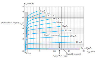 |
Fig.8: Output Characteristic Curve (Ref. 2)
- It is the graph between the output current IC to the output voltage VCE for a range of values of input current IB.
- It has three basic regions:
Active Region
- Here, the base-emitter junction is forward biased and collector base junction is reverse biased.
- These are the same conditions that existed in the active region of the common base configuration.
- This can be employed for voltage, current or power amplification.
Cut-off Region
- Here IC is not equal to zero when IB is zero.
- For linear amplification purposes, it is defined as IC = ICEO .
- The region below IB = 0µA is to be avoided for undistorted output signal.
- When the transistor is used as a switch, the condition should be ideally IC = 0mA for a chosen VCE voltage.
Saturation Region
- It is the region that lies towards the left of VCE = 0V.
Common Collector Configuration
- The notation and symbols of npn and pnp transistors are given below:
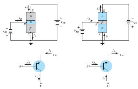 |
Fig. 9: NPN CC and PNP CC (Ref. 2)
- In the above figure all the currents are shown in their actual conventional directions.
- It is used for impedence matching purposes as it has high input impedence and low output impedence.
- It can be designed using common emitter characteristics.
- The output characteristics of common collector is same as that of common emitter configuration for all practical purposes.
- The output characteristics are a plot between IE versus VCE for all values of IB.
- The input current of common collector is same as that of common emitter configuration.
- Here the region of operation will ensure that maximum ratings are not being exceeded and output ratings have minimum distortion.
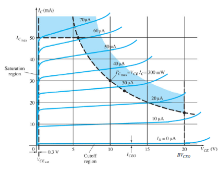 |
Fig.10: Output Characteristic Curve (Ref. 2)
- The characteristics specifying the minimum VCE that can be applied without entering the non-linear region is saturation region.
- The maximum power dissipation is given by,
P = VCE . IC
Key takeaway
 |
Q1) In a CB IE= 2mA, IC=1.5mA. Calculate IB?
Sol: IE =IB+IC
2= IB+1.5
IB=0.5mA
Q2) In a CB current amplification factor is 0.9. If emitter current is 1.2mA. Determine the value of base current?
Sol: α = 0.9
IE =1.2mA
α = IC/ IE
IC = α IE =0.9 x 1.2 = 1.08mA
IE =IB+IC
1.2= IB+1.08
IB= 0.12mA
Q3) In a CB connection IC=1.0mA and IB= 0.02mA. Find the value of current amplification factor?
Sol: IE =IB+IC =1+0.02 = 1.02mA
α = IC/ IE
α = 1.0/1.02 = 0.98
Q4) In a CB connection the emitter current is 0.98mA. If the emitter circuit is open the collector current becomes 40 A. Find total collector current. α =0.92
Sol: ICBO=40 A
A
IC = α IE+ICBO
= (0.92 x 0.98x10-3) + 40x10-6
IC =0.94mA
Q5) In a common base connection, α = 0.95. The voltage drop across 3 kΩ resistance which is connected in the collector is 2.5 V. Find the base current.
Sol: IC = 2.5/3000 = 0.83mA
α = IC/ IE
IE = IC/α =0.83/0.95=0.87mA
IE =IB+IC
0.87 =IB+0.83
IB=0.04mA
Q6) Find the value of β if (i) α = 0.9 (ii) α = 0.98 (iii) α = 0.99.
Sol:  = α/1- α = 0.9/1-0.9 = 9
 = α/1- α = 0.98/1-0.98 = 49
 = α/1- α = 0.99/1-0.99 = 99
Q7) The collector leakage current in a transistor is 200 μA in CE arrangement. If now the transistor is connected in CB arrangement, what will be the leakage current? Given that β = 120.
Sol: ICEO=200 μA
 = 120
= 120
α = /1+
/1+ = 120/121=0.99
ICEO=ICBO/1- α
ICBO= 1.6 μA
Q8) For a certain transistor, IB = 18 μA; IC = 2 mA and β = 60. Calculate ICBO.
Sol: IC =  IB+ICEO
ICEO= IC -  IB= 2x10⁻³-(60x18x10-6) = 0.92mA
α = /1+
/1+ = 60/61=0.98
ICBO= (1- α) ICEO = (1-0.98)x 0.92=15.08 μA
The hybrid two port model is shown below.
 |
Fig 11 Hybrid model of transistor
Vi = h11Ii + h12Vo
Io = h21Ii + h22Vo
h11 = hi = Vi/Io for Vo =0 [Input resistance]
h12 = hr = Vi/Vo for Ii =0 [Reverse voltage gain]
h21 = hf = Io/Ii for Vo =0 [forward current gain]
h22 = ho = Io/Vo for Ii =0 [output admittance]
The hybrid equivalent model is shown below
 |
Fig 12 hybrid equivalent mode
The transistor model has three terminals with two ports.
hi = input resistance
ho= output conductance
hr= Vi/Vo = reverse transfer voltage
hf= Io/Ii = forward transfer current ratio
The simplified model is shown below
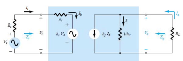 |
Fig 13 Simplified model
Finding current gain Ai
Applying KCL at the output of above circuit
Io =I + hf Ib = Vo ho + hf Ib
Vo = -Io RL
Io = -Io RL ho + hf Ib
Io (1 + RL ho) = hf Ib
Ai = Io/ Ib = hf/(1 + RL ho)
Finding Voltage Gain AV
Applying KVL at input of the above h-model
Vi = hi Ib + hr Vo
But Ib = (1 + ho RL)/hf
Io = - Vo/RL
Substituting in above equation and solving for Vo/Vi we get
Av = - hf RL/hi + (hi ho- hf hr) RL
Finding Input Impedance Zi
Vi = hi Ib + hr Vo
Io = - Vo/RL
Ai = Io/ Ib
Vi = hi Ib - hrRLAiIb
Zi = Vi/Ib = hi - hrRLAi
Finding Output impedance Zo
It is ratio of output voltage to output current with Vs =0
Io = Voho + hfIb
Ii = -hrVo/Rs + hi
Zo = Vo/Io = 1/[ho – (hfhr/hi+ Rs)]
Key takeaway
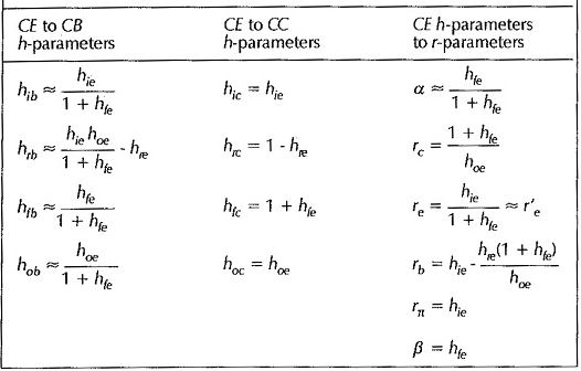
Table of hybrid parameters for CE, CB and CC
 |
It is used for voltage amplification. There are two capacitors one is coupling capacitor Cc connected to output of first stage and base of second stage. The resistances R1, R2 and RE are biasing and stabilisation network. The capacitor CC blocks DC signal and transmits AC signals.
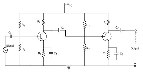 |
Fig 14 RC Coupled Amplifier
When AC signal is applied to base of first transistor it is amplified and appears across its collector Rc. This signal id fed to base of next stage. The second stage amplifies the signal and is received through RL.
Frequency Response: At low frequency the reactance of CC is high and hence very small part of signal passes from first stage to second. At high frequency the reactance of CC is small and it behaves as short circuit. The capacitive reactance of base-emitter junction is low and causes decrease in current amplification factor  . At mid-frequency the voltage gain is constant. As frequency increases gain increases as reactance of CC decreases. This result is higher loading effect of first stage to the next and hence gain decreases. These two factors cancel each other and result in uniform gain.
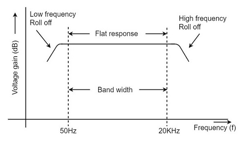 |
Fig 15 Frequency Response of RC coupled Amplifier
Key takeaway
It is used for voltage amplification. There are two capacitors one is coupling capacitor Cc connected to output of first stage and base of second stage. At low frequency the reactance of CC is high and hence very small part of signal passes from first stage to second. At high frequency the reactance of CC is small and it behaves as short circuit. The capacitive reactance of base-emitter junction is low and causes decrease in current amplification factor  .
.
The mid band gain of transistor is the transistors gain at its mid frequencies where the transistors gain is at the highest.
The mid band gain is the most important region of transistor amplification. This is because this is the region of frequencies where a transistor produces a constant and high level of gain. When a transistor is rated for its gain or amplification factor, it is the mid band region that this is referring to.
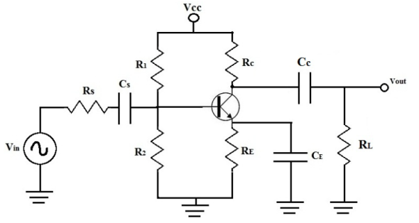 Fig 16 Transistor for mid band gain  Fig 17 AC equivalent Circuit of transistor for mid band gain
|
The mid band gain of the transistor circuit is
AM = Vout/Vin
Let us consider the below circuit.
Now calculating the impedance
RB = R1||R2 = [(R1+R2)/R1R2]
Now the value of resistance RB’ is
RB’ = RB||r = [(RB r
 )/ RB r
 ]
]
The value of output resistance RL’
RL’ = r0||Rc||RL
The value of voltage drops across r is
is
V = [RB’Vin/(RB’+RS)]
The reduced circuit now can be redrawn as
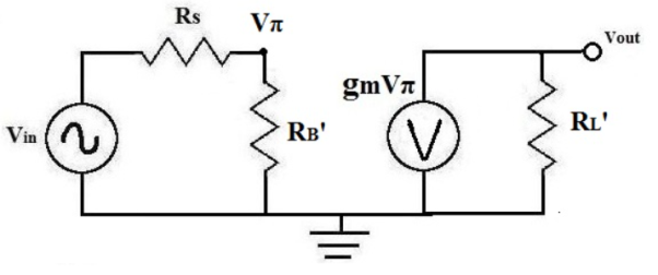 |
Fig 18 Reduced Equivalent Circuit
Vout = -gm V RL’= - gm RL’[RB’Vin/(RB’+RS)]
The mid-band gain is given as
AM= Vout/Vin = - gm RL’[RB’Vin/(RB’+RS)]/Vin
AM= - gm RL’[RB’/(RB’+RS)]
Key takeaway
The value of output resistance RL’
RL’ = r0||Rc||RL
The value of voltage drops across r is
is
V = [RB’Vin/(RB’+RS)]
The mid-band gain is given as
AM= - gm RL’[RB’/(RB’+RS)]
 |
1.6.1 Emitter Follower
This is also called as common collector amplifier. It is basically used to provide current gain and for impedance matching. The circuit is shown below where the input is applied through base and output is obtained from emitter. The voltage gain is always<1 and output voltage are in phase with input voltage. The output follows the input hence it is called as emitter follower.
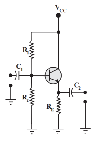 |
Fig 19 Emitter Follower
The base voltage can be obtained by applying voltage division rule on R2 and R1
VB =  VCC
VCC
The emitter voltage is VE = VB – 0.7
The emitter current is IE = 
VCEQ = VCC-VE
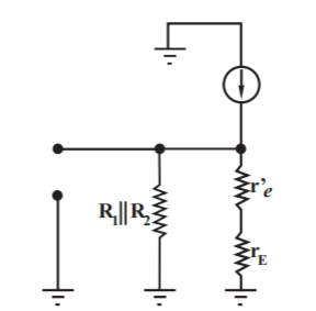
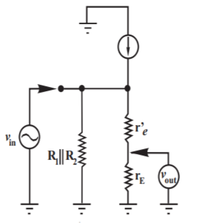
For A.C analysis the circuit can be drawn as shown below
|
Fig 20 A.C equivalent circuit
The total equivalent ac emitter resistance is rE which is
rE = RE||RL
- The voltage gain AV = rE/(re’ +rE)
Practically re’ << rE. The voltage gain then becomes
AV = 1
- Current Gain Ai = hfe (Zin rE/Zbase RL)
This relationship is due to the current divisions that occur in both the input and output circuits. We have used in place of hfe. We are assuming that is approximately equal to hfe. The subscript “c” merely indicates that the parameter applies to the emitter follower (common collector) rather than the common emitter amplifier. The exact equation for hfc is
hfc = hfe +1
Since is normally much greater than 1, we normally assume that they are approximately equal.
- Input Impedance Zin = R1||R2||Zbase
- Base Input Impedance Zbase = hfe (re’+rE)
Where:
hfe= transistor current gain
re’= the ac emitter resistance
rE = RL||RE
- Output Impedance (Zout)
The output impedance is the impedance that the circuit presents to its load. When a load is connected to the circuit, the output impedance of the circuit acts as the source impedance for that load.
Zout = RE|| [re’ + (Rin’/hfe)]
1.6.2 Darlington Pair –
The Darlington pair is a combination of two common collector cascade configuration. In Darlington pair the collectors of the two transistors are connected together, emitter of Q1 is connected to the base of Q2 and emitter of Q2 acts as the emitter of Darlington connection.
The important feature of the Darlington connection is that the composite will act as a single unit, the current gain of which is equal to the product of the individual current gains β1 and β2 .
Fig 21: Darlington connection of transistors
In general Darlington connection with more than 2 transistors is not used because
1) With increase in transistors, leakage current increases.
2) The voltage gain of CC is approximately 1 but that of the Darlington is much less than 1. With increase in transistor, voltage gain will decrease further.
Advantages:
1) Very high current gain.
2) Very low voltage gain.
3) Very high input impendence.
4) Very low output impendence.
Disadvantage – more than 2 transistors cannot be used.
Analysis of Darlington emitter follower –
The circuit diagram of the Darlington emitter follower is shown above.
Assumptions –
1) Both Q1 and Q2 are identical.
2) hoe  0.1 i.e. approximate analysis.
3) hfe RE >> hie
1.Current gain of the Darlington emitter follower (AI):
a) current gain of Q2 :
AI2  = (1 + hfe)
b) current gain of Q1 :
The input resistance of stage 2 acts as the load for Q1
 Ri2 = hie + (1 + hfe)RL2
= hie + AI2RE {where RL2 = RE}
As Ri2 is large, the condition hoe RL’ < 0.1 is not satisfied by first stage
Where RL’ = RL2 = RE
Hence using exact analysis for Q1
 AI1 =
AI1 = 
Substitute  and
and  , we get
 AI1 =
AI1 =  -------------(1)
But  hence, RL1 = Ri2 = hie + hfeRE
Substituting the expression for RL1 in equation (1)
AI1 = 
hoehie is very small so neglecting it,
AI1 = 
Overall current gain : AI = 
i.e. AI = AI1  AI2
AI2
= 
AI -------------(2)
The above equation shows that overall current gain of the Darlington connection is much higher than that of the single emitter follower (common collector).
2.Overall input resistance (Ri) :
The overall input resistance will be same as the input resistance of first stage Q1
 Ri = Ri1
Ri1 = hie + AI1RL1 where RL1 = Ri2
Substituting the value of AI1 and Ri2, we get
Ri1 = hie RE --------------(3)
2nd term in equation (3) is much larger than first term, so neglecting hie
Input resistance, Ri1 = RE
RE
If hoehfeRE << 1, then
Ri1 = RE ----------------(4)
For a single CC amplifier Ri = hie +  RE
RE
Equation (4) shows that due to Darlington connection, there is tremendous increase in input resistance.
3.Voltage Gain of Darlington connection (AV) :
Overall voltage gain AV = 
AV2 is calculated using approximate analysis.
AV1 is obtained by exact analysis.
a) Voltage gain AV2 = 
AI2 = 1 + hfe
Ri2 = hie + (1 + hfe)RL2
RL2 = RE
 {Adding and subtracting hie in numerator}
AV2 = 1  ----------(5)
b) Voltage gain AV1: AV1 = AI1
But for single emitter follower,
AI1 = (1 + hFe),
Ri1 = hie + AI1RL1
AV1 =  where RL1 = Ri2
Adding and subtracting hie in numerator of right-hand side, we get
AV1 = 
AV1 = 1 - 
AV1 = 1 -  -----------(6)
Overall voltage gain = AV = AV1 × AV2
i.e. AV = AV2 = 
AV = 
It is evident that Ri1 >> Ri2 hence 3rd and 4th term in above equation can be neglected
AV = 1 -  -------------(7)
Comparing (5) and (7)
AV  AV2
AV2
The overall voltage gain is approximately equal to the voltage gain of second stage.
4.Overall output resistance RO :
The overall output resistance of the emitter follower Darlington circuit is same as the output resistance of second stage.
YO = hoc 
Hence YO2 = hOC 
Hence YO2 = hOC 
RS for 2nd stage is R01 i.e. output resistance of 1st stage.
But hrc = 1 , hOC = hOe , hFC = - (1 + hFe) and hiC = hie
YO2 = hoe + 
Neglect hOe because we are performing approximate analysis for the second stage we get,
YO2 = 
Hence, RO2 = 
But, RO1 = 

RO = RO2 =  +
+ 
Neglect the 2nd term due to  in denominator

The above equation tells us that the RO of Darlington emitter follower is much less than that of a single emitter follower.
Key takeaway
For emitter follower
The value of Z is typically higher than the common emitter amplifier. The voltage gain is always less than 1 The heavy swamping of the circuit virtually eliminates the effect of r’ on the voltage gain.
Que. For T1 hie1 = 6 KΩ hFe1 = 80 hre1 = hoe1 = 0
For T2 hie2 = 1 KΩ hFe2 = 100 hre2 = hoe2 = 0
For the Darlington pair emitter follower, shown in figure, determine:
a) Input impendence R1
b) Voltage gain VO / VS
c) Current gain IO / IS
d) Output impendence
Sol – Given: hie1 = 6 KΩ hFe1 = 80 hre1 = hoe1 = 0
hie2 = 1 KΩ hFe2 = 100 hre2 = hoe2 = 0
Amplifier configuration:
Q1 → CC Q2 → CC
Therefore, approximate analysis is used, for both stages
For second stage:
Current gain (Ai2)
AI2 =  = 1 + 100 = 101
Input resistance (Ri2)
RL1 = Ri2 = hie2 + (1 + hFe2)RL = 1 × 10³ + (1 + 100) × 103 = 102 KΩ
Voltage gain (AV2):
AV2 =  =1 -
=1 -  0.99
0.99
For first stage:
Current gain (Ai1):
Ai1 = 1 + hFe1 = 81
Input resistance (Ri1):
Ri1 = hie1 + (1 + hFe1 )RL
= 6 × 10³ + (1 + 80) × 102 × 103 = 8.268 MΩ
Voltage gain (AV1):
AV1 =  = 1 -
= 1 -  0.999
0.999
RO1 =  86.42 Ω
RO2 =  10.76 Ω
Overall voltage gain (AV):
AV = AV1 × AV2 = 0.999 × 0.99 = 0.989
AVS
Figure shows equivalent circuit of the input side
 0.998
0.998
AVS = 0.989 × 0.998 = 0.987
Overall voltage gain:
AI = Ai = Ai1 × Ai2 = 81 × 101 = 8181 Ans.
Input impendence:
Ri = 0.89 MΩ Ans.
Overall voltage gain:
AV = 0.989 Ans.
Voltage gain include source:
AVS = 0.987 Ans.
Output Impendence:
RO = 10.76 Ω Ans.
Que. For the bootstrap circuit shown, calculate AI , Ri and AV. The transistor parameters are hie = 2 KΩ , hFe = 100 ,  = 40 K and hre = 2.5 × 10⁻⁴.
Sol – Given : hie = 2 KΩ , hFe = 100 ,  = 40 K , hre = 2.5 × 10⁻⁴.
Amplifier configuration : common emitter with Re
AC analysis : For a.c. Analysis of amplifier we consider the d.c. Supply voltage as ground and capacitor as short circuit and apply Miller’s theorem across feedback resistor (10K) then modified circuit is given as :
The circuit down in fig. (a) represents a CE amplifier. But to analyse the bootstrapped element we need to consider the CC voltage gain first.
AV =  common collector voltage gain
RL’ = 2K || 4K || 4K ||  1 K || 490 K = 1 KΩ
Assume AV  0.98
0.98
Checking approximation :
hoeRL’  0.1
0.1
0.025 < 0.1
Hence , valid approximation
Approximate analysis :
AI = 1 + hFe = 101
Ri = hie + (1 + hFe)RL’ = 2 + 101 = 103 KΩ Ans.
AV = AI = 0.98
From fig. (a) : R1  500 KΩ
Now, fig. (a) can be analysed by CE and the modified circuit is given as,
Checking approximation :
hoe (Re + RL)  0.1
0.1

Hence, valid approximation
Approximate analysis :
AI’=  -hFe = -100
Ri’= hie + (1 + hFe)Re’ = 2 + 101 × 1 = 103 KΩ
AV’ = 
AV = AV’ = -2.9126
From fig. (b) : Ri = Ri’ || 500K = 100 || 500 = 85.406 KΩ
AI = 
= (-1) × 100 × 
From fig. (c) :  -
-  = 0.8291
Hence, AI = - 100 × 0.82918 = -82.918
Que. The bootstrapped Darlington pair uses identical transistors with the following h-parameters.
hie = 1 KΩ , hre = 2.5 × 10⁻⁴ , hoe = 2.5 × 10⁻⁴ A/V , hFe = 100
Find 
Sol - Given : hie = 1 KΩ , hre = 2.5 × 10⁻⁴ , hoe = 2.5 × 10⁻⁴ A/V , hFe = 100
Q1 – CC , Q2 - CC
For a.c. Analysis of amplifier we consider the d.c. supply voltage as ground and capacitor as short circuit.
Apply Miller’s theorem across R3 = (100K)
Voltage Gain :
AV =  AV1 × AV2
Let us assume AV = 0.98
Where ,  = 4900 KΩ
RL’ = 0.1K || 82K || 10K ||  0.1 K || 82 K || 10 K || 4900 K = 0.0988 KΩ
Analysis for Q2 [CC] :
Checking approximation :
hoeRL’ =  0.0988 = 2.47 × 10⁻³ < 0.1
Approximate analysis :
AI2 = 1 + hFe = 101
Ri2 = hie + (1 + hFe)RL’ = 1 + 101 × 0.0988 = 10.9788 KΩ
AV2 = AI2 = 0.908915
Analysis for Q1 [CC] :
RL = Ri2
hoeRL1 =  = 0.27447 > 0.1
Exact analysis :
AI2 =  = 79.2486
Ri1 = hie + AI1hrcRL1 = 1 + 79.2486 × 10.9788
= 871.054 KΩ (hrc  1)
1)
AV1 = 
= 0.99885
AV  AV1 × AV2 = 0.99885 × 0.908915
= 0.9079 (Ans)
Ri = R || Ri1 = 1085.78 || 871.054 {Fig. (a)}
= 483.32 KΩ
 AI1 = 79.2486
AI = 
= 


AI = (-0.9889) × (-101) × (-1) × (-79.2486) × 0.55487
= 4391.94 (Ans)
Equation for VO/Vi :
Analysis of Q2 [CC] :
hoe(Re+RL)
 ×[0.0988 + 1] = 0.02747 < 0.1
Approximate analysis
AI2 = - hFe = -100
Ri2 = hie + (1 + hFe)Re
= 1 +(1 + 100)0.0988 = 10.9788 KΩ
AV2 =  =
=  -9.1084
Analysis of Q1 [CC] :
RL1 = Ri2 = 10.9788 KΩ
hoeRL1 =  = 0.27447 > 0.1
Exact analysis :
AI1 =  = 79.2486
RL1 = hie + AI1RL1 = 1 + 79.2486 × 10.9788
= 871.054 KΩ
AV1 =  =
= 
 AV = AV1 × AV2 = -9.0975
Hence, -AI1 =  79.248

Ri = 483.32 KΩ
 -9.0975 (Ans)
Que. A bootstrapped Darlington amplifier shown in fig. Uses identical transistor with h-parameters, hie = 1.5 KΩ , hoe = 50 μA/V. If the circuit is to have Ri of 268 MΩ. Find the value of hFe for the transistor used.
Sol – Given : hie = 1.5 KΩ , hoe = 50 μA/V, Ri = 2.68 MΩ, R1 = 1 MΩ , R2 = 1 MΩ , Re2 = 1 KΩ
RLeft = RC1 || RC2 = ∞ || 1 K = 1 KΩ
Amplifier configuration : bootstrapped Darlington pair amplifier [CC - CC]
Checking for approximation :
hoeRLeft  0.1
0.1
hoeRLeft = 25 × 10-6 × 1 K = 0.025 < 0.1
Which is less than 0.1
Approximate analysis :
Calculation for hFe
Ai2 = 1 + hFe
Ri2 = hie2 + Ai2RLeft = 1.5 K + (1 + hFe)1 K
Ai1= 1 + hFe
Ri1 = hie1 + Ai1RL1
Where RL1 = Ri2
Ri1 = 1.5K + (1 + hFe)[1.5K + (1 + hFe)1K]
2.68 MΩ = 1.5K + 1.5K + (1 + hFe)1K + 1.5Khfe + (1+hFe) 1KhFe
= 3K + 1K + 1KhFe + 1.5KhFe + 1KhFe + 1KhFe2
= 4K + 3.5KhFe + 1KhFe2
= (4 + 3.5hFe + hFe2) × 103
 hFe2 + 3.5hFe + 4 = 2680
 hFe2 + 3.5hFe - 2676 = 0
The quadratic equation can be solved as,
hFe = 
Substituting values we get,
hFe 
=  50 or -53.5
hFe is always positive.
 hFe = 50 Ans.
Overall voltage gain :
(AV) : AV = AV1 × AV2 = ( 1 -  )( 1 -
  )
)
= ( 1 -  )( 1 -
  )
)
= 0.999 × 0.971 = 0.97
Overall current gain –
Ai = Ai1 × Ai2
= (1 + hFe) (1 + hFe)
= (51)(51)
= 26.01
Key takeaway
Sr. No. | Parameter | Expression |
1 | Current gain (AI) | AI  |
2 | Input resistance (Ri) | Ri =  |
3 | Voltage gain (AV) | AV = 1 -  |
4 | Output resistance (RO) | RO =   |
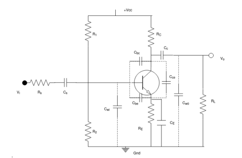 Fig 22 Transistor model  Fig 23 Hybrid equivalent pi-model
|
Ci = cwi + cbe + cbc( 1-av) Co = cwo + cce + cbc( 1-AV)
= cwi + cbe + cmi = cwo + cce + cmo
Where cmi = input miller capacitance where cmo = o/p miller capacitance
At increasing frequencies, the reactance xc will decrease in magnitude resulting in a shorting effect across the output and a decrease in gain.
For high frequency response, various parasite capacitances (cbe, cbc, cce) of the transistors are included along with the wiring capacitors ( cwi, cwo) for analysis.
For high frequency response, cs, cc, ce are assumed to be in short circuit state.
Input capacitance ci includes wiring capacitance cwi, the transistor capacitance.
Cbe and miller capacitance cmi.
The o/p capacitance co includes wiring cce and miller capacitance cmo
Cmi = cbc (1-av)
Cmo = cbc (1−11−1/av)
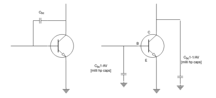
|
Fig 24 Output capacitance
For the input network, the – 3db frequency is defined by

Rthi = rsrs // r1r1 // r2r2 // rππ
Ci = cwi + cbc + cmi
Cmi = cbc (1-av)
At very high frequency, the effect of ci is to reduce the total impedance of the parallel combination of r1r1, r2r2 , rπrπ & ci. The route is a reduced level of voltage across ci, a reduction in In and a gain for the system.

Rtho = rc // rlrl // re
c0c0 = cwot + cce + cmo
Cme = cbe ( 1 - 1av)1av)
∵∵ 1 >> yav cmo = cbc
At very high frequency, XCO will decrease and consequently reduced the total impedance of o/p parallel branches. The net result is vo will also decline towards ‘o’ as the reactance xc becomes (zero) or smaller.
Reference:
1 “Electronic Devices and Circuit Theory”, Boylestad and Nashelsky, PEARSON
PUBLICATION.
2 “Electronic devices and circuits”, Salivahanan, Suresh Kumar, Vallavaraj,
TMH, 1999
3 “Integrated Electronics, Analog and Digital Circuits and Systems”, J. Millman
And Halkias, TMH, 2000
4 “Micro Electronic Circuits”, Sedra and Smith, Oxford University Press, 2000
5 “Electronic Devices and Circuits”, David A Bell, Oxford University Press, 2000