Unit-4
Oscillators
In many of the electronic applications, electrical energy at a specific frequency is required. It is done with the help of a device called on oscillator. An oscillator is just an electronic circuit which converts Dc energy into Ac energy of required frequency. It can produce oscillation of frequency ranging from small values to extremely high value (100MHz). It is a static device with no moving parts.
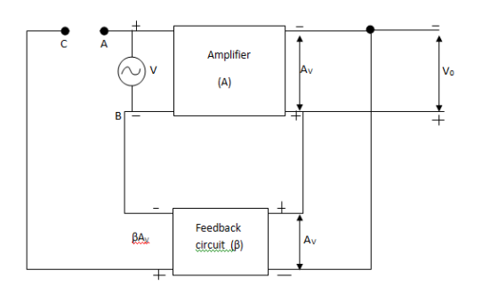 |
Positive feedback amplifier as an Oscillator- An oscillator is a device that generates AC output signals without any input AC signal. A fraction of output is feedback to the input.
Fig 1 Positive Feedback Circuit
A= Gain of amplifier (open 100Þ)
Β= Feedback gain
V= input signal
Av= Amplified signal at output
A fraction of the signal βAv is feedback to the input. It must be ensured by the feedback circuit that feedback signal βAv must be in phase with input signal v.
Now C is connected to A and input signal is removed. The only signal which is to drive the amplifier is feedback (βAv)
Case (1)- If βA<1, βAv>V and the output signal will die out (damped oscillation)
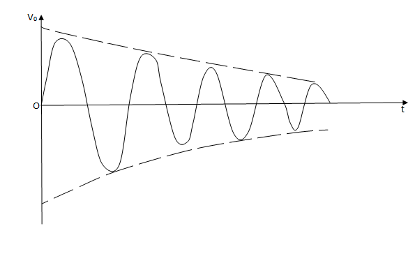 |
Fig 2 Damped Oscillations
Case (2)- If βA>1, βAv>V and the output signal will built up (growing oscillations)
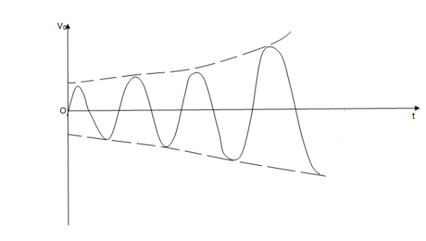 |
Fig 3 Growing Oscillations
Case(3)- If βA=1, no change occurs in the output and we get an output with constant magnitude (undamped or Sustained oscillations)
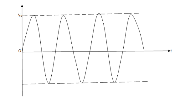 |
Fig 4 Sustained Oscillations
Thus to obtain Sustained oscillations, the loop gain βA of a positive feedback amplifier must be unity(1).
Derivation of overall gain of positive feedback amplifier
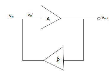 |
Fig 5 Positive Feedback
V= Vin + β Vout
Vout = Av1
Vout = A(Vin+β Vout )
Vout (1-Aβ)= AVin
Or 

 AF=
AF= 
Barkhausen Condition – Condition that are required to be satisfied to operate the circuit as an oscillator are called as Barkhausen condition.
In oscillator circuit there is no input signal hence the feedback signal it say should be sufficient to maintain the oscillations.
Barkhausen condition states that
- The loop gain (Aβ) is equal to unity i.e.
 =1
=1 - The phase shift around the loop is zero or an inteqer multiple of 2
 , i.e. <βA = 2n
Where n=0,1,2,……..
Key takeaway
Barkhausen condition states that
- The loop gain (Aβ) is equal to unity i.e.
 =1
=1 - The phase shift around the loop is zero or an inteqer multiple of 2
 , i.e. <βA = 2n
These are known as harmonic oscillators and are LC tuned feedback or RC tuned feedback type oscillators that generate purely sinusoidal waveform which is constant in amplitude and frequency.
RC phase-shift oscillators use resistor-capacitor (RC) network as shown in Figure below to provide the phase-shift required by the feedback signal. They have excellent frequency stability and can yield a pure sine wave for a wide range of loads.
 |
Fig 6 RC network
Ideally a simple RC network is expected to have an output which leads the input by 90o.The phase-difference will be less than this as the capacitor used in the circuit cannot be ideal.
Mathematically the phase angle of the RC network is expressed as
ɸ = tan -1 Xc / R
where, XC = 1/(2πfC) is the reactance of the capacitor C and R is the resistor. In oscillators, these kind of RC phase-shift networks, each offering a definite phase-shift can be cascaded to satisfy the phase-shift condition led by the Barkhausen Criterion.
LC Oscillators:
These are positive feedback oscillators. These oscillators produce regenerative feedback at the required frequency with the circuit components L, C and R forming a tank circuit. This feedback network is an attenuation network which has a gain of less than one ( β <1 ) and starts oscillations when Aβ >1 which returns to unity ( Aβ =1 ). The oscillator frequency is controlled by LC with the circuit output frequency.
The working of LC tank circuit is explained below. The simple way to understand the working is by understanding the working of components L and C. The capacitor stores the electrostatic energy in the form of potential, the inductor stores energy in its coil in the form of electromagnetic energy.
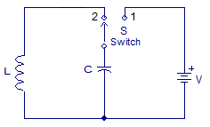 |
Fig 7: LC Tank Circuit
The capacitor is charged to voltage V, after it gets fully charged the switch changes its position. This charged capacitor then discharges itself through the inductor. The current through L increases and voltage across C decreases. As there is now no external voltage in the circuit to maintain the current within the coil, it starts to fall as the electromagnetic field begins to collapse.
A back emf is induced in the coil (e = -Ldi/dt) keeping the current flowing in the original direction. This current charge up capacitor, C with the opposite polarity to its original charge. C continues to charge up until the current reduces to zero and the electromagnetic field of the coil has collapsed completely. The above process is repeated and the LC oscillator works.
The frequency of oscillator voltage depends on L and C. The circuit is at resonance when XC =XL. The resonant frequency curve is shown below.
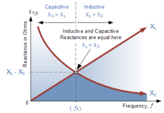 |
Fig 8: Resonant Curve
XL = 2 f L
f L
XC = 
At resonance XL = XC
2 f L =
f L = 
The resonant frequency is then given as
fr = 
LC oscillator using BJT
Here the LC circuit is connected across the load. The coil L2 is connected between base and emitter of transistor which is mutually coupled with coil L. Due to mutual induction the current flowing in one is induced in the other.
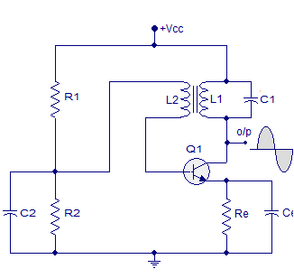 |
Fig 9 LC Oscillator using BJT
The electromagnetic energy is transferred from coil L to coil L2 and a voltage of the same frequency as that in the tuned circuit is applied between the base and emitter of the transistor. The circuit impedance at oscillation is resistive and the CB voltages are 180o out of phase. So, additional 180o phase shift is introduced through feedback path.
Key takeaway
These are known as harmonic oscillators and are LC tuned feedback or RC tuned feedback type oscillators that generate purely sinusoidal waveform which is constant in amplitude and frequency.
A typical RC phase shift oscillator using transistor as an active device is shown below
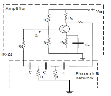 |
Fig 10 RC phase shift oscillator
The output V0of the single stage CE amplifier has been connected as an input to the RC phase shift network. The output of the phase shift network is connected at the input of the amplifier.
As the amplifier is CE type it introduces phase shift of 180°. The phase shift network will introduce an additional 180° phase shift
Resistance R3 + Zi = R
Where Ziis input impedance of CE amplifier
Zi = hie || (R1 || R2)
Therefore, R1 and R2 are large, we can neglect them
Therefore Zi = hie
So R3 = R- hie
Frequency of Oscillations is given by
F =  *
*  where k =
Derivation: voltage source.
 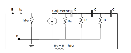 |
For this transistor is replaced by hybrid model and current source is replaced by
Fig 11 Hybrid Model of RC phase shift circuit
Replace R3 + hie = R and Rc= KR
Apply KVL tw various loops
Loop I therefore hfe IbRc + I1 Rc +  + I1 R – I2 R =0
Where RC = KR
hfe IbkR+ I1kR +  + I1 R – I2 R =0
Put S = jw
I1 – I2R = - I2R = - hfe IbkR ………(1)
Loop 2 :-  + I2R – I3R + I2R – I1R = 0
Put S = jw
I2 – I1R – I3R =0 …………….(2)
Loop 3:-  + I3R + I3R – I2R = 0
Put S = jw
I3 – I2R = 0 ……………..(3)
Rearranging (1), (2) and (3)
I1 – I2R = - hfeIb kR
-I1R + I2 – I3R = 0
And
-I2R + I3 = 0
= 0
Solving above equation for I3 using Cramer’s rule
 =
= 
I3= 
∆ =  - R2
- R2 -R2
-R2
∆ =  -
-  -
- 
∆ = 
Simplifying we get,
∆ = 
 =
= 
 = -hfe IbkR × R2 = - K hfeIb R3
I3=  ………..(4)
 Aββ =
Aββ =  but IC = hfeIb
β = 
Gain A =  = hfe
= hfe
Therefore Aβ =  × hfe =
Substituting valve of I3 from (4)
Aβ = 
Put S = jw , then S2= -w2, S3 = -w2, S3 = -jw3
Aβ = 
Dividing the numerator and denominator by –jw3R3C3 we get,
Aβ = 
Substituting  = X
= X
Aβ = 
According to Barkhausen Criterion <Aβ = 0° for that the imaginary term of the denominator should be equal to 0
i.e.
X3-4kx-6x = 0
X(X2 -4k -6) = 0
X=0 or X2 = 4k + 6 or X = 
 =
= 
Or W = 
Or F = 
This is the required expression of frequency
Key takeaway
Frequency of Oscillations is given by
F =  *
*  where k =
Please refer above section.
The Wien -bridge oscillator
In this, phase shift is produced by using 2 transistors. Each produces a phase shift of 180° and hence phase shift of 360° is obtained
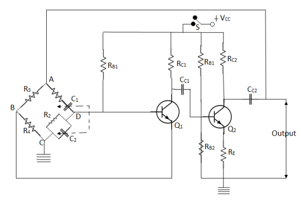 |
Fig 12 Wein Bridge Oscillator
It is a 2 stage amplifier with R-C bridge circuit. The bridge circuit has 4 arms each containing components R1C1 in Series, R2 C2 in parallel, R3 and R4. Q1 acts as an oscillator and amplifier where as Q2 Serves as an inverter
When circuit is closed through switch S, the bridge circuit produces the oscillations of frequency whose expression is given by-
F= 
If R1=R2=R and C1= C2 = C then
F = 
A total phase shift of 360° is obtained at the output of the second transistor. A fraction of this output energy is fed back to the oscillatory circuit (bridge) at the upper terminal. This positive feedback is to meet with the losses in the oscillator and hence undamped oscillations are produced.
Advantages-
- It has better stability
- Output is constant
- Overall gain is high
- Frequency can be adjusted by varying C1 and C2
Disadvantages-
- Costly
- Cannot generate frequency>1MHz.
Que) In the RC network of a Weinbridge oscillator R1 = R2 = 200kΩ, determine the value of each of the capacitor to obtain a frequency of 5kHz.
Solution-
F = 
F = 5kHz, = 5000Hz
R1= R2= 200kΩ = 200×103Ω
5000 = 
C =  = 159.15 pF
Expression for feedback factor (β) and frequency (f)
In order to obtain expression for β and f, we will consider only frequency sensitive arms AD and CD as shown in figure below
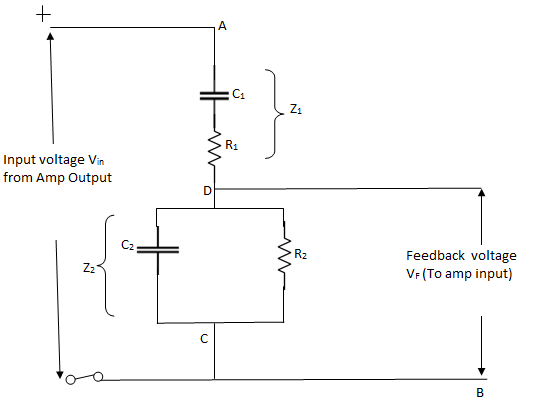 |
Vin is actually the output voltage V0which comes from the amplifier output and voltage across R2C2acts as a feedback voltage VF
Feedback factor β = 
Let impedance of arm AD be Z1 and that of DC be Z2
Therefore VF =  ×Vin{ using voltage divider}
β =  =
=  ………….(1)
Z1= R1 +  =
=  …………..(2)
Z2 = R2 || Xc2=  =
=  ………….(3)
Substituting equation (2) and (3) in (1)
β = 
Substituting jw = S
β = 
β = 
β = 
β = 
Resubstitute jw = S , S2 = j2 w2 = -w2
β = 
β = 
Rationalize the above equation
β =  ……………(4)
The phase shift introduced by the wien bridge circuit at the desired output frequency should be 0°. For that the imaginary part of equation (4) should have a zero value.
WC1R2(1-w2R1R2C1C2) = 0
w2R1R2C1C2 = 1
 =
= 
W = 
F = 
The above equation is the expression for the oscillator frequency.
If we substitute R1 = R2 = R and C1 = C2 = C
F =  or w =
For β, if R1 = R2 = R, C1= C2 = C
β = 
Substituting
W = 
β =  =
=  =
= 
Thus, at the oscillator frequency F, the value of feedback factor β is 
Key takeaway
- It has better stability
- Output is constant
- Overall gain is high
- Frequency can be adjusted by varying C1 and C2
Crystal Oscillator can be designed by connecting the crystal into the circuit such that it offers low impedance when operated in series-resonant mode and high impedance when operated in anti-resonant or parallel resonant mode as shown below in figure a and b respectively.
 |
Fig 13(a) Series Resonance Fig 13(b) Parallel Resonance
In the circuits shown, the resistor R1 and R2 form the voltage divider network while the emitter resistor RE stabilizes the circuit. Further, CE (Figure a) acts as an AC bypass capacitor while the coupling capacitor CC (Figure a) is used to block DC signal propagation between the collector and the base terminals. Next, the capacitors C1 and C2 form the capacitive voltage divider network in the case of Figure b.
In addition, there is also a Radio Frequency Coil (RFC) in the circuits (both in Figure a and b) which offers dual advantage as it provides even the DC bias as well as frees the circuit-output from being affected by the AC signal on the power lines.
On supplying the power to the oscillator, the amplitude of the oscillations in the circuit increases until a point is reached wherein the nonlinearities in the amplifier reduce the loop gain to unity. Next, on reaching the steady-state, the crystal in the feedback loop highly influences the frequency of the operating circuit.
Further, here, the frequency will self-adjust so as to facilitate the crystal to present a reactance to the circuit such that the Barkhausen phase requirement is fulfilled.
In general, the frequency of the crystal oscillators will be fixed to be the crystal’s fundamental or characteristic frequency which will be decided by the physical size and shape of the crystal.
However, if the crystal is non-parallel or of non-uniform thickness, then it might resonate at multiple frequencies, resulting in harmonics. Further, the crystal oscillators can be tuned to either even or odd harmonic of the fundamental frequency, which are called Harmonic and Overtone Oscillators, respectively.
Key takeaway
Crystal Oscillator can be designed by connecting the crystal into the circuit such that it offers low impedance when operated in series-resonant mode and high impedance when operated in anti-resonant or parallel resonant mode.
Hartley Oscillator
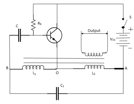 |
It is most popular oscillator and is commonly used in radio receivers. It consists of 2 coil L1 and L2 wound over the same core. Thus, mutual inductance exists between terms. A capacitor C1 is connected to from L-C circuit. Rb provides the necessary biasing. The capacitor C block DC component.
Fig 14 Hartley Oscillator
The frequency of oscillation is determined by L1,L2, and C1.
When Switch C1 discharge through L1 and L2, setting up oscillation of frequency f, given by
F =  =
= 
The oscillation between 0 and B drives the transistor and output appears at the collector which supplies the losses.
It may be noted that L1 and L2 are magnetically linked with each other so that points B and A are 180° out of phase. A further shift of 180° is produced by transistor. Thus, it ensures proper positive feedback and results in undamped oscillations.
Que2) In a transistor Hartley oscillator if L1 = 0.1 m H, L2 = 10  H and mutual inductance between the two coil M = 20
  H, calculate the value of capacitor C1 of oscillatory circuit to obtain frequency of 4110 kHz
Sol-
L1 = 100  H
H
L2 = 10  H
H
M = 20  H
H
Total inductance, L = L1 + L2 + 2M
= 100 + 10 + 2 × 20
= 150  H
H
F = 
4110× 103 = 
 × 150 × 10-6 × C =
C =  = 10pf
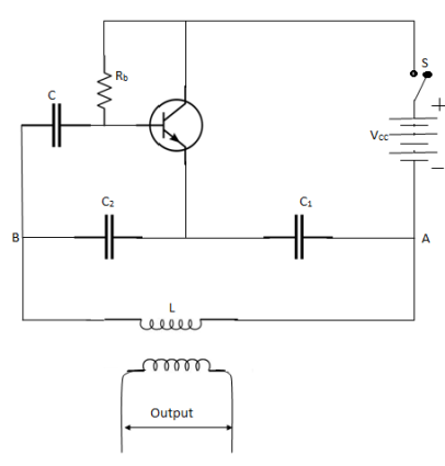 |
Colpitt’s Oscillator – It is similar to Hartley. The only difference is that in case of Colpitt’s oscillator, coupling is capacitive instead of being inductive.
Fig 15 Colpitts Oscillator
In this the tank circuit consist of inductor L in parallel with 2 capacitors C1 and C2 which are in series. The resistor Rb provider the necessary biasing and capacitor C blocks the d.c. Component. The frequency of oscillations is given by
F = 
Where CT – Total Capacitance 
When switch S is closed, capacitor C1 and C2 are charged. These capacitors discharge through L, setting up of oscillation of frequency F
The oscillation across C2 is applied to transistor which gets amplified. This amplified output is fed to the oscillatory circuit in order to supply the losses. In this way it ensures undamped oscillations.
A phase difference of 180° is created between A and B and a further phase shift of 180° is produced by transistor action.
Que) Find the operating frequency of a transistor Colpitt’s oscillator if C1 = 30 pf, C2 = 60Þf and L = 10  H
H
Sol- Total capacitance, CT =  =
=  = 20 pf = 20× 10-12 F
Inductance, L = 10 H = 10× 10-6 H
F = 
=  = 11.25 MH
Clapp’s Oscillator
This oscillator has only one difference from Colpitts that C3 capacitor is added in the tank circuit a shown below.
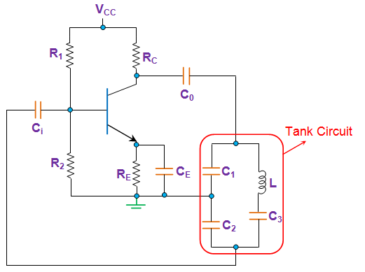 |
Fig 16 Clapp Oscillator
The working is similar to Colpitts Oscillator and the frequency of oscillation is given by
f = 
Usually, the value of C3 is chosen to be much smaller than the other two capacitors. This is because, at higher frequencies, smaller the C3, larger will be the inductor, which eases the implementation as well as reduces the influence of stray inductance.
Nevertheless, the value of C3 is to be chosen with utmost care. This is because, if it is chosen to be very small, then the oscillations will not be generated as the L-C branch will fail to have a net inductive reactance. However, here it is to be noted that when C3 is chosen to be smaller in comparison with C1 and C2, the net capacitance governing the circuit will be more dependent on it.
The approximate value of frequency is
f = 
The Clapp Oscillator can be used for variable frequency.
Key takeaway
The frequency of the oscillations is determined by the value of the capacitors and inductor in the tank circuit. Thus, the main difference between a Colpitts Oscillator and a Hartley Oscillator is that the former uses tapped capacitance, while the latter uses tapped inductance.
Reference:
1 “Electronic Devices and Circuit Theory”, Boylestad and Nashelsky, PEARSON
PUBLICATION.
2 “Electronic devices and circuits”, Salivahanan, Suresh Kumar, Vallavaraj,
TMH, 1999
3 “Integrated Electronics, Analog and Digital Circuits and Systems”, J. Millman
And Halkias, TMH, 2000
4 “Micro Electronic Circuits”, Sedra and Smith, Oxford University Press, 2000
5 “Electronic Devices and Circuits”, David A Bell, Oxford University Press, 2000