Unit-5
Power Amplifiers
When a transistor conducts current between collector and emitter, it also drops voltage between those two points. At any given time, the power dissipated by a transistor is equal to the product of collector current and collector-emitter voltage. Just like resistors, transistors are rated for how many watts each can safely dissipate without sustaining damage.
High temperature is the mortal enemy of all semiconductor devices, and bipolar transistors tend to be more susceptible to thermal damage than most. Power ratings are always referenced to the temperature of ambient (surrounding) air. When transistors are to be used in hotter environments >25o, their power ratings must be derated to avoid a shortened service life.
The position of the Q-point and the extent of the characteristics that is being used, decides the class of operation of power amplifiers.
The various classes of power amplifiers are –
(i ) Class A power amplifier
(ii ) Class B power amplifier
( iii ) Class C power amplifier
( iv ) Class AB power amplifier
1). The intersection of the output characteristics curve and the load line is known as operating point or Q-point of transistor.
2). On this quiescent operating point, if an a.c. Signal is superimposed by the application of a.c. Sinusoidal voltage at the input, the base current varies sinusoidally about its quiescent value IBQ.
3). Since the transistor is biased to operate in the active region, the output is linearly proportional to the input i.e. IC = βIB
4). Hence the collector current also varies sinusoidally about its quiescent value IBQ.
Class A amplifier: A class-A amplifier is the amplifier in which the Q-point of the input signal are selected such that the output signal is obtained for a full input cycle. For this purpose, the position of the Q-point is approximately at the midpoint of the load line.
For all the values of the input signal, the transistor remains in the active region and never enters into cut-off or saturation region.
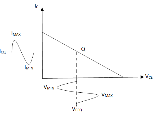 |
Fig 1 Output characteristics of CE Amplifier
The collector current IC flow for complete 3600 (full cycle) of the input cycle. Thus, the angle of the collector current flow is 3600.
Class A amplifier are of 2 types –
( i ) Directly coupled class A amplifier – In directly coupled type, the load is directly connected in the collector circuit.
( ii ) Transformer coupled class A amplifier – In this the load is coupled to the collector using a transformer called an output transformer.
( i ) Directly coupled class A amplifier –
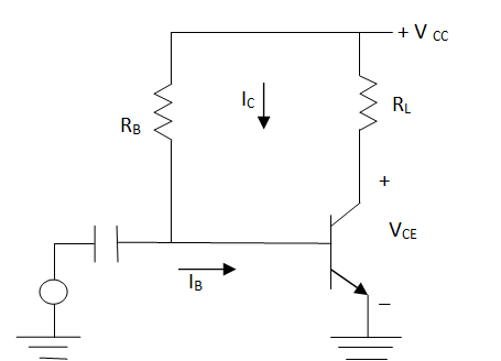 |
Fig 2 Directly coupled class A amplifier
The value of RB is selected such that Q point lies at the centre of d.c. Load line.
VCC = ICRL + VCE
IBQ = VCC – 0.7 / RB
ICQ = βIBQ
VCEQ = VCC - ICQRL
DC power input : PDC = VCCICQ Watts
The d.c. Power input is provided by the supply:
- With no a.c. Input signal, the d.c. current drawn is the collector bias current ICQ.
- Even if any a.c. Input signal is applied, the average current drawn from the d.c. supply remains same.
A.C. Power Output:
Vpp = Vmax - Vmin
Vmin = Min instantaneous value of collector output voltage
Vmax = Max instantaneous value of collector output voltage
Vpp = Peak of a.c. Output voltage
Vm = Vpp / 2 = Vmax – Vmin / 2 = Amplitude of a.c. Output voltage
Im = Ipp / 2 = Imax – Imin / 2
The r.m.s value of alternating output voltage and current is given as
Vrms = Vm / √2 ;Irms = Im / √2
Pac = VrmsIrms = I2rmsRL = V2rms / RL
Pac = Vm /√ 2 : Im /√ 2 = 1/2Vmax – Vmin /√ 2 . Imax – Imin /√ 2
Pac = ( Vmax - Vmin )( Imax - Imin ) / 8
Efficiency:
% n = Pac / Pdc x 100 %
= [(Vmax - Vmin) (Imax - Imin) / 8 x Vcc x ICQ] x 100%
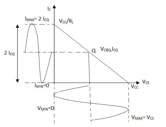 |
Fig 3 AC Power Output
Maximum Efficiency:
Vmax = Vcc, Vmin = 0
Imax = 2ICQ, Imin = 0 { As Q is in middle }
n = (Vmax - Vmin) (Imax - Imin) / 8 x Vcc. ICQ x 100 %
= (Vcc - 0)(2ICQ - 0) / 8 x Vcc.ICQ x 100 %
Nmax = 25 % { Biggest disadvantage }
Power dissipation ( Pd ) : Pd = Pdc - Pac
Power dissipation = D.C. Power input – AC power output
( i ) When there is no input signal, then Pac = 0 and the entire d.c power gets dissipated in the form of heat which is maximum PD.
(Pd)max = PDC = VCCICQ when Pac = 0
( ii ) When input signal is larger, more power is delivered to load ( Pac is more ) and less is the power dissipation.
Thus class A amplifier dissipated less power when delivers maximum power to the load while it dissipates maximum power while delivering zero power to the load.
Disadvantages:
( i ) The load resistance is connected directly to collector, hence quiescent current passes through this resistance. This current represents a considerable waste of power, since it doesn’t contribute to the a.c. Component of the power. Also it is inadvisable to pass the d.c. Component of current through the output device.
( ii ) Efficiency is poor.
( ii ) Transformer coupled Amplifier :
Generally the output impedance of the transistor is much higher than the input impedance ( RL ) of the loudspeaker. Hence most of the power generated would be lost in the transistor.
To transfer a significant amount of power to the load, it is necessary to use an output matching transistor.
Applying KVL : VCC – VCEQ = 0 => VCEQ = VCC
DC power input : PDC = VCCICQ
Where,
RL = load on secondary
R2 = Reflected load on the primary or effective load as seen by primary
RL1 = ( N1 / N2 )2 RL
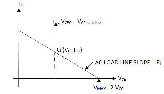 |
Fig 4 Load Line
AC power output Pac :
Pac = (Vmax - Vmin) (Imax - Imin) / 8
Pac = I12rmsRL1 = I22rmsRL = V1rmsI1rms = V2rmsI2rms
Where V1rms = RMS value of primary voltage
V2rms = RMS value of secondary voltage
Efficiency (n) : n = Pac / Pdc x 100 %
Max efficiency :
Vmin = 0, Vmax = 2VCC
Imin = 0, Imax = 2ICQ
% nmax = 50 %
Class B amplifier– In class B amplifiers, the Q point and the input signal is selected, such that the output signal is obtained only for one half cycle for a full input cycle.
Either the quiescent current or the quiescent voltage is approximately zero. If quiescent current is zero, then the transistor is in cut off region, and the transistor remains in active region only for the half cycle of the input signal. Hence at output we get only the half cycle.
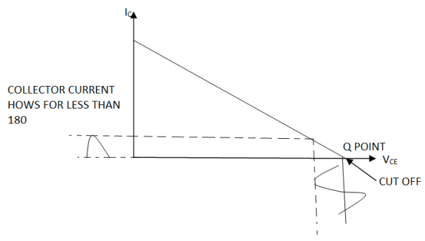 |
Fig 5 Load line characteristics of class B amplifier
If instead of ICQ = 0, we would have taken VCEQ = 0( i.e. Q point on Y-axis ) then the transistor would have been in saturation region and the collector current flows only for negative half cycle of the input signal.
Efficiency of this mode is higher than class A mode.
Since in this mode, collector current flows only for half cycle, so that output signal is distorted. To get the full cycle, a pair of transistors is used in class B operation. The 2 transistors conduct in alternate half cycles of the input signal abd so a full cycle across the load is obtained. The two transistors are identical in characteristics and are called matched transistors.
Depending upon the types of 2 transistors, the two different circuit configurations of Class B are –
( i ) Push Pull Class B amplifier
( ii ) Complimentary Symmetry Class B
( i ) Push Pull Class B amplifier : When both the transistors are of some type i.e. either n-p-n or p-n-p, then the circuit is called push-pull class B audio frequency power amplifier.
The push pull circuit requires 2 transformers, one as input transformer called driver transformer and the other to connect the load called output transformer. The input signal is applied to the primary of the driver transformer. Both the transformer is centre tapped transformers.
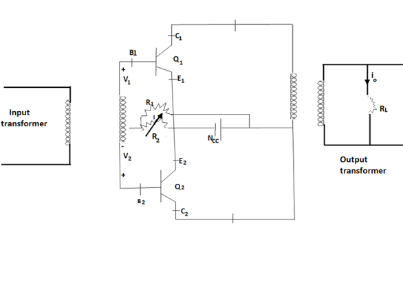 |
Fig 6 Push pull amplifier
In the circuit, both Q1 and Q2 are of n-p-n type. p-n-p can also be used but with -VCC. Both are in CE configuration.
Operation:
Case ( i ) – During positive half cycle,
Q1 = ON, Q2 = OFF
IO1α iC1
 |
Fig 7 Positive half cycle output
Case ( ii ) – During negative half cycle,
Q1 = OFF, Q2 = ON
IO2α iC2
 |
Fig 8 Positive half cycle output
Case ( iii ) When signal is absent i.e. V1 = V2 = 0
If R2 = 0 then,
VBE1 = VBE2 = 0
Both Q1, Q2 are in cut off [ Class B operation]
Case ( iv ) If R2 increases then IR2 increases and when IR2 = Vr then
VBE1 = VBE2 = Vr [ Class AB operation]
Case ( v ) If R2 increases more, then IR2 increases VBE increases and Q point will move towards saturation.
The total d.c. Power is given by,
Pdc = VCC x Idc
= 2 / ∏ VCC Im
a.c. Power, Pac = Vrms.Irms
= I2rmsR1L = V2rms / R1L
Efficiency:
% n = Pac / Pdc x 100 %
= ( Vm.Im / 2 ) / 2 / ∏VCCIm
% n = ∏ / 4 Vm / VCC x 100 %
Max Efficiency:
Max efficiency is possible only if, Vm = VCC
% nmax = ∏ / 4 VCC / Vcc x 100 = 78.5 %
Power dissipation:
Pd = Pdc - Pac
= 2 / ∏ VCCIm - Vm.Im / 2
= 2 / ∏ VCCVm/ R1L - Vm2 / 2 R1L
Maximum power dissipation:
For max power dissipation,
DPd / dVm = 2 / ∏ VCC / R1L - 2Vm/ 2 R1L = 0
2 / ∏ VCC / R1L = Vm/ R1L
Vm = 2 / ∏ VCC
This is the condition for max power dissipation,
Hence max power dissipation is given by,
(Pd)max= 2 / ∏ VCC x 2 / ∏ VCC / R1L - 4 / ∏2 VCC2 / 2R1L
= 4 / ∏2 VCC2 / R1L - 2 / ∏2 VCC2 / R1L
(Pd)max= 2 / ∏2 VCC2 / R1L
For max efficiency Vm = VCC hence the dissipation is not maximum when the efficiency is maximum and when power dissipation is maximum, efficiency is not maximum.
The a.c. Power is given by,
Pac = Vm2 / 2RL1
Where Vm = VCC is the maximum condition.
The maximum a.c. Power is given by
(Pac)max = VCC2 / 2RL1
(Pd)max = 2VCC2 / ∏2RL1 = 4 / ∏2( VCC2 / 2RL1 )
(Pd)max = 4 / ∏2 (Pac)max
The maximum power dissipation per transistor is given by,
(Pd)max per transistor = 4 / ∏2 (Pac)max / 2
= 2 / ∏2 (Pac)max
Advantages:
- Efficiency is much higher than the class A operation.
- When there is no input signal, the power dissipation is zero.
- Ripples present in supply voltage also get eliminated.
- Due to transformers, impedance matching is possible.
Disadvantages:
- 2 centre tap transformers are necessary
- Transformers make the circuit bulky and costlier.
- Frequency response is poor.
- Complementary Symmetry Class B push pull amplifier –
This circuit is transformer less circuit. But with common emitter configuration, it becomes difficult to match the output impedance for maximum power transfer with output transformer. Hence the matched pair of complementary transistors is used in common collector (emitter follower) configuration in this circuit.
This is because common collector configuration has lowest output impedance and hence the impedance matching is possible.
 |
Fig 9 Complimentary symmetry Push pull amplifier
The circuit is driven from a dual supply of +-VCC. The transistor Q1 is n-p-n while Q2 is p-n-p type.
Operation:
During positive half cycle:
 |
Fig 10 Positive half cycle operation
During negative half cycle:
 |
Fig 11 Negative half cycle operation
Cross over distortion :
 |
Fig 13 Crossover Distortion
Advantages:
(i) As the circuit is transformer less, its weight, size and cost are less.
(ii) Due to common collector configuration, impedance matching is possible.
(iii) The frequency response improves due to transformer less class B amplifier circuit.
Disadvantages:
(i) The circuit needs two separate voltage supplies.
(ii) The output is distorted to cross-over distortion.
Class AB amplifiers (between A and B):
In class AB amplifiers, the Q-point and the input signal are selected such that the output signal is obtained for more than a half cycle but less than a full cycle.
 |
Fig 14 Characteristic curve for class AB operation
The Q point is below the midpoint but above X-axis or above the midpoint but to the right of Y-axis. Its efficiency is more than class A but less than class B. Efficiency increases as the Q-point moves away from the centre of the load line.
Key takeaway
 |
Numerical:
Q-1 – Determine the input power, output power and efficiency resulting in a class B push-pull amplifier providing a signal 20V peak to a 16 Ω load, using a single supply of VCC = 30V.
Soln.Given: VL(p) = 20 V, RL = 16 Ω, VCC = 30 V
The input power is given by,
Pi(dc) = VCC(2 / ∏ I / p) = VCC.2 / ∏.VL(p) / RL
= 30 x 2 / ∏ x 20 / 16 = 23.87 W Ans.
The output power is given by,
PO(ac) = VL2(p) / 2RL = VL2(rms) / 2RL = (20)2 / 2 x 16 = 12.5 W Ans.
Thus efficiency is given by,
n = PO(ac) / Pi(dc) x 100 = 12.5 / 23.87 x 100 = 52.37 % Ans.
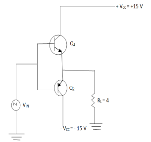
Q-2 – Class B complementary A.F. Power amplifier shown in the below figure
 |
Calculate:
- Maximum a.c. Power which can be developed.
- Collector dissipation while developing maximum a.c. Power.
- Efficiency
- Maximum power dissipation per transistor.
- Efficiency under maximum power dissipation condition Assume sinusoidal input.
Soln.Given: VC = 15 V, RL = 4 Ω
Use the expression derived for push pull class B.
- The maximum a.c. Power is,
(Pac)max = 1/2VCC2 / RL = 1/2(15)2 / 4 = 28.125 W Ans
- When power developed is maximum, Vm = VCC
RL = Vm / Im
Im= Vm / RL = VCC / RL = 15 / 4 = 3.75 A
Pdc = 2 / ∏VCCIm = 2 / ∏ x 1.5 x 3.75 = 35.809 W
Pd = Pdc – Pac = 35.809 – 28.125 = 7.684 W Ans.
This is the total collector dissipation under maximum power conditions.
- Efficiency:
% n = Pac / Pdc x 100 = 28.125 / 38.809 x 100 = 78.5 % Ans.
The efficiency is maximum possible for class B, due to the fact that the power developed is at its maximum.
- For maximum power dissipation,
Vm = 2 / ∏ VCC = 2 / ∏ x 15 = 9.5492 V
Im = Vm / RL = 9.5492 / 4 = 2.3873 A
Pdc = 2 / ∏ VCC Im= 2 / ∏ x 15 x 2.3873 = 22.797 W
While Pac = 1/2Vm2 / RL = 1/2(9.5492)2 / 4 = 11.398 W
(Pd)max = Pdc – Pac = 22.797 – 11.398 = 11.39 W
(Pd)max = 11.39 / 2 = 5.699 W [ Per transistor]
Alternatively, we can directly use the result,
(Pd)max = 2 / ∏2 (Pac)max per transistor
= 2 / ∏2 x 28.125 = 5.699 W per transistor Ans.
- Efficiency under (Pd)max condition,
% n = Pac under (Pd)max / Pdc under (Pd)max x 100
= 11.398 / 22.797 x 100 = 50 % Ans.
This shows that when efficiency is maximum, power dissipation is not maximum and when power dissipation is maximum, efficiency is not maximum.
Q-3 – (A ) A series fed class A amplifier uses a supply voltage of 10 V and load resistance of 20 Ω. The a.c. Input voltage results in a base current of 4 mA peak. Calculate,
- D.C. Input power
- A.C. Output power
- % efficiency
Assume β of the transistor as 25 and the collector bias current of 50 mA.
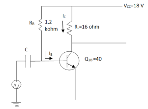
(B) Calculate the input power, output power & the efficiency of class A amplifier shown in figure. The input voltage causes a base current 5mA rms.
 |
Sol :(A) Given : VCC = 10 V, (ib)m = 4 mA, β = 25, ICQ = 50 mA, RL = 20 Ω
- D.C. Input power :
PDC = VCCICQ = 10 x 50 x 10-3 = 0.5 W Ans.
- A.C. Output power :
(ic)m = β(ib)m = 25 x 4 = 100 mA
But ic is the output current I.
Im = 100 mA
Pac = I2mRL / 2 = (100 x 10-3)2 x 20 / 2 = 0.1 W Ans.
- % Efficiency :
% n = Pac / Pdc x 100 = 0.1 / 0.5 x 100 = 20 % Ans
(B) Given class A amplifier is shown in below figure
 |
Current IBQ can be written as,
IBQ = VCC – 0.7 / RB = 18 – 0.7 / 1.2 x 103 = 14.4167 mA
Now, ICQ = βIBQ = 40 x 14.4167 = 576.67 mA
And, VCEQ = VCC – ICQ RL = 18 – 576.67 x 10-7 x 16 = 8.7733 V
So, Pdc = VCCICQ = 18 x 576.67 = 10.38 W Ans.
This is the input power.
(Ib)rms = 5 mA
(Ic)rms = β(Ib)rms = 40 x 5 = 200 mA
This is nothing but the output collector current r.m.s value Irms.
Irms = 200 mA
Output power can be written as,
Pac = I2rms RL = (200 x 10-3) x 16 = 640 mW
This is the power delivered to the load.
Hence the efficiency of the amplifier is,
% n = Pac / Pdc x 100 = 640 x 10-3 / 10.38 x 100
% n = 6.165 % Ans.
Q-4 - For a class B amplifier using common collector configuration, the supply voltage is 25 V while the load resistance is 16 Ω. If the input a.c. Signal of 20 V peak is su[[lied, determine the input power, output power and the efficiency.
Sol.Given: VCC = 25 V, Vm = 20 V, RL = 16 Ω
For a common collector configuration, the voltage is 1.
Vin(peak) = Vout(peak) = 20 V
Now, Vm / Im = RL
Im = Vm / RL = 20 / 16 = 1.25 A
The input power is given by,
PDC = 2 / ∏ = VCCIm = 2 / ∏ x 25 x 1.25 = 19.8943 W Ans.
The output power is given by,
Pac = Vm Im / 2 = 20 x 1.25 / 2 = 12.5 W Ans.
Thus, efficiency is given by,
% n = Pac / Pdc x 100 = 12.5 / 19.8943 x 100 = 62.832 % Ans.
( i ) Push Pull Class B amplifier : When both the transistors are of some type i.e. either n-p-n or p-n-p, then the circuit is called push-pull class B audio frequency power amplifier.
The push pull circuit requires 2 transformers, one as input transformer called driver transformer and the other to connect the load called output transformer. The input signal is applied to the primary of the driver transformer. Both the transformer are centre tapped transformers.
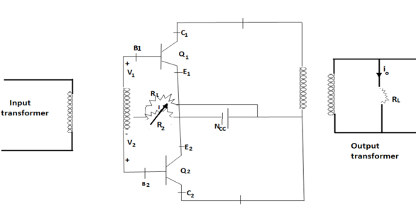 |
Fig 15 Push pull amplifier
In the circuit, both Q1 and Q2 are of n-p-n type. p-n-p can also be used but with -VCC. Both are in CE configuration.
Operation:
Case ( i ) – During positive half cycle,
Q1 = ON, Q2 = OFF
IO1α iC1
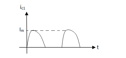 |
Case ( ii ) – During negative half cycle,
Q1 = OFF, Q2 = ON
IO2α iC2
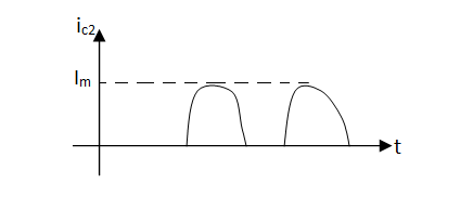 |
Case ( iii ) When signal is absent i.e. V1 = V2 = 0
If R2 = 0 then,
VBE1 = VBE2 = 0
Both Q1, Q2 are in cut off [ Class B operation]
Case ( iv ) If R2 increases then IR2 increases and when IR2 = Vr then
VBE1 = VBE2 = Vr [ Class AB operation]
Case ( v ) If R2 increases more, then IR2 increases VBE increases and Q point will move towards saturation.
The total d.c. Power is given by,
Pdc = VCC x Idc
= 2 / ∏ VCC Im
a.c. Power, Pac = Vrms.Irms
= I2rmsR1L = V2rms / R1L
Efficiency:
% n = Pac / Pdc x 100 %
= ( Vm.Im / 2 ) / 2 / ∏VCCIm
% n = ∏ / 4 Vm / VCC x 100 %
Max Efficiency:
Max efficiency is possible only if, Vm = VCC
% nmax = ∏ / 4 VCC / Vcc x 100 = 78.5 %
Power dissipation:
Pd = Pdc - Pac
= 2 / ∏ VCCIm - Vm.Im / 2
= 2 / ∏ VCCVm/ R1L - Vm2 / 2 R1L
Maximum power dissipation:
For max power dissipation,
DPd / dVm = 2 / ∏ VCC / R1L - 2Vm/ 2 R1L = 0
2 / ∏ VCC / R1L = Vm/ R1L
Vm = 2 / ∏ VCC
This is the condition for max power dissipation,
Hence max power dissipation is given by,
(Pd)max= 2 / ∏ VCC x 2 / ∏ VCC / R1L - 4 / ∏2 VCC2 / 2R1L
= 4 / ∏2 VCC2 / R1L - 2 / ∏2 VCC2 / R1L
(Pd)max= 2 / ∏2 VCC2 / R1L
For max efficiency Vm = VCC hence the dissipation is not maximum when the efficiency is maximum and when power dissipation is maximum, efficiency is not maximum.
The a.c. Power is given by,
Pac = Vm2 / 2RL1
Where Vm = VCC is the maximum condition.
The maximum a.c. Power is given by
(Pac)max = VCC2 / 2RL1
(Pd)max = 2VCC2 / ∏2RL1 = 4 / ∏2( VCC2 / 2RL1 )
(Pd)max = 4 / ∏2 (Pac)max
The maximum power dissipation per transistor is given by,
(Pd)max per transistor = 4 / ∏2 (Pac)max / 2
= 2 / ∏2 (Pac)max
Advantages:
- Efficiency is much higher than the class A operation.
- When there is no input signal, the power dissipation is zero.
- Ripples present in supply voltage also get eliminated.
- Due to transformers, impedance matching is possible.
Disadvantages:
- 2 centre tap transformers are necessary
- Transformers make the circuit bulky and costlier.
- Frequency response is poor.
- Complementary Symmetry Class B push pull amplifier –
This circuit is transformer less circuit. But with common emitter configuration, it becomes difficult to match the output impedance for maximum power transfer with output transformer. Hence the matched pair of complementary transistors is used in common collector (emitter follower) configuration in this circuit.
This is because common collector configuration has lowest output impedance and hence the impedance matching is possible.
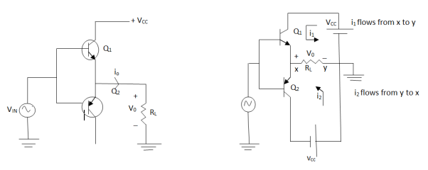 |
Fig 16 Complimentary symmetry Class B push pull amplifier
The circuit is driven from a dual supply of +-VCC. The transistor Q1 is n-p-n while Q2 is p-n-p type.
Operation:
During positive half cycle:
 |
Fig 17 Positive half cycle operation
During negative half cycle:
 |
Fig 18 Negative half cycle operation
Cross over distortion:
 |
Advantages:
(iv) As the circuit is transformer less, its weight, size and cost are less.
(v) Due to common collector configuration, impedance matching is possible.
(vi) The frequency response improves due to transformer less class B amplifier circuit.
Disadvantages:
(iii) The circuit needs two separate voltage supplies.
(iv) The output is distorted to cross-over distortion.
The application of a sinusoidal signal to the input of an ideal amplifier will result in a sinusoidal output wave. Generally, the output wave is not an exact replica of the input signal waveform because of various types of errors. The types of distortion that may exist are –
( i ) Non-linear distortion –We have assumed that the dynamic transfer wave for the transistor is linear i.e. IC = βIB. But the transfer curve is nonlinear of the form,
IC = K1IB + K2IB2 + K3IB3 + - - -
Due to this, the new frequencies at the output is produced which are not present in the input. This type of distortion is sometime referred as ‘amplitude distortion’.
( ii ) Frequency distortion –This type of distortion exist when the signal components of different frequencies are amplified differently.
( iii ) Phase-Shift distortion -It results from the unequal phase shifts of the signals of different frequencies.
Please refer section 5.2 for the detailed analysis.
Sometimes during amplification, it is necessary to select the desired frequency band and reject rest. Desired frequency band and reject rest. For this reason, tuned amplifiers are needed.
Tuning means selecting i.e. in this ride by amplitudes frequency selection is done by using a tuned or resonant circuit at the load. Tuned or resonant circuit at the load. Tuned amplifiers are used for the amplification of a specific frequency signal or a narrowband frequency signal.
An audio amplifier is unable to select a particular frequency signal. Thus, an audio amplifier is not used for the radio frequency signal amplification.
Tuned Circuit and resonant frequency in tuned amplifiers-
As tuned circuit possers the property of resonance. Thus, it allows selection of a particular range of frequency. The resonant frequency of the tuned circuit will be the centre frequency of the detected frequency band.
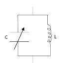 |
Fig 20 Tunned circuit
Tunned amplifiers provided high gain. This is so because a resonant circuit as a load offers high impedance and gain of transistor is dependent on load impedance.
Tuned amplifiers are basically designed for narrow bandwidth frequency signal. The resonance frequency of a tuned circuit
Is given as
Fr = 1/2π √LC
The frequency response curve for a tuned amplifier is given as-
Voltage gain
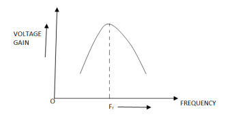 |
Fig 21 Voltage Frequency Response
The above graph shows that the response of tuned amplifier is maximum at resonant frequency ( Fr))
Basic circuit of a tuned amplifier
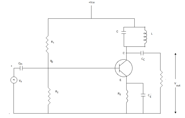 |
Fig 22 Tuned Amplifier
In this amplifier circuit the tuned circuit is connected as a load output is taken across it
Resonance Circuit: The frequency at which inductive reactance become equal to Capacitive reactance, the circuit behaves as purely resistive. This phenomenon is known as resonance and the particular frequency is known as resonant frequency.
Quality factor = at is defined as the ratio of coil impedance of an inductor to its resistance for a better Q factor, resistance must be low.
It is basically measuring the purity of an inductor and is a unitless quantity.
Ø=Xl/R
= 2πfr L/ R
Where fr = 1/= 2π√LC
Bandwidth of tuned amplifiers – It is defined as that frequency range where the gain of the amplifier reduces, to 70.7 % of its highest value
Relation between Ø and BW is given by
Ø = fr/BW
Classification of Tuned amplifiers-
Tuned Amplifiers
Small signal amplifier
Large signal amplifier
Single tuned amplifier
Double tunnel amplifier
Stagger tuned amplifiers
Large signal tuned amplifiers-
These are used for amplification purpose but for the radio frequency signal having a large magnitude as it requires large power for operations, thus operated under class B or C operation.
Small Signal tuned amplifiers- they are used to amplify signals of small magnitude for its operation is small, thus operated under class A operation
Further these are classified as (1) single tuned
(2) Double tuned
(3) stagger tuned
Single Tuned Amplifiers:
Single tuned amplifiers are multistage amplifier circuit that employs a parallel tuned circuit as load. However, the tuned circuit in each stage is require to be tuned to similar frequencies.
CE configuration can be used as a single tuned amplifier which includes which includes the parallel tuned circuit.
Construction:
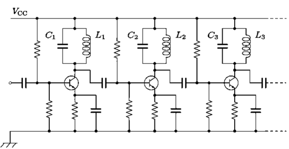 |
Fig 22 Single Tuned Amplifier
The Figure shows the Circuit arrangement of a single tuned amplifier will capacitive coupling.
It is noted that for a tuned circuit, capacitance and inductance value must be so selected that the frequency of resonance must be equivalent to the frequency of the applied signal.
The Capacitor CE employed is bypass capacitor where as biasing and stabilization circuits are followed by R1, R2 and RE.
Tunned LC circuit employed in the collector region asts as the load.
Capacitor is taken variable to vary resonant frequency large signal amplification can be obtained it the frequency of input signal is similar to the frequency of resonance of LC circuit.
Operation:it high frequency signal is applied at the base emitter terminal of the transistor
By varying the capacitor in tuned circuit, the resonant frequency of the circuit can be made equivalent to the frequency of the frequency of the applied input signal. Here, the high impedance is offered to the signal frequency by the tuned circuit. Thus, a large output is achieved.
For an input signal will multiple frequencies only the frequency that corresponds to resonant frequency will get amplified while all other frequencies are rejected by the LC circuit
Hence only the desired frequency signal gets selected and thus amplified by the circuit.
Voltage gain and frequency signal gets selected and thus amplified by the circuit.
Voltage gain and frequency response:
For a tuned amplifier, voltage gain is given
AV = BRac/rm
= BL/CR/rm
Ar = BL/ CRrm
Where Rac:. Impedance of tuned circuit
Rin = input impedance
Diagram
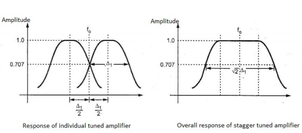 |
Fig 23 Frequency response curve
As we know that the impedance of the circuit is very high and is entirely resistance in nature at resonant frequency. Thus, the maximum at resonant frequency (Fr)
BW = F2 - F1 =Fr/ø
Any frequency with in this range will be amplified by the amplifier.
Advantages:
- It possesses a good signal noise ratio.
- It provides variable bandwidth for signs amplification.
- As it provides ratio wave transmission hence used in radio transmitter and receiver.
Disadvantages:
1) The overall circuity is costly as well bulky due to the presence of inductor and capacitors in tuned circuits.
2) Amplification in the range of the audio frequency cannot be achieved.
3) Increase in Bandwidth leads to complexity in the circuit.
Potential instability in tuned Amplifiers: It is a limitation of tuned amplifiers that result in the bad reproduction of signals.
At tuned amplifier must possess high selective nature. For that ø factor must also be high this high ø will provide a high voltage gain with the reduction in bandwidth.
:. BW = Fr/ ø
This reduction in Bandwidth will deteriorate the quality of amplification Due to this, the complete band of the signal will not be equally, amplified. There by resulting in bad reproduction of the signal. This is known as potential instability.
Double Tuned Amplifiers:
The figure below shows the coupling section of a transformer coupled double tuned amplifier. There is one more simplified figure given below in which the current source is placed in place of transistor. R1 is in series with L1. The C1 and L1 form the tank circuit on the primary side. The L2 and C2 form tank circuit on the secondary side.
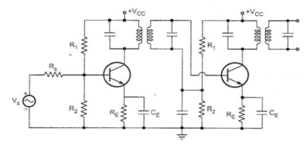 |
Fig 24 Double Tuned Circuit
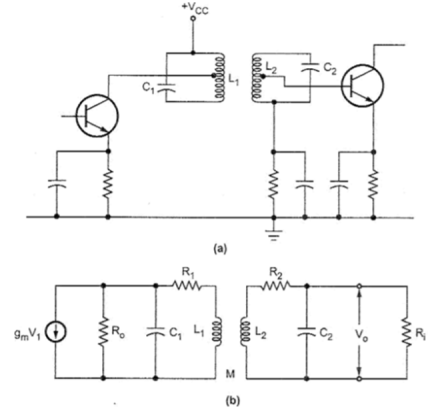 |
Fig 25 Simplified Circuit for Double tuned amplifier
The figure below shows the simplified equivalent model where the series and parallel resistances are combined into series elements.
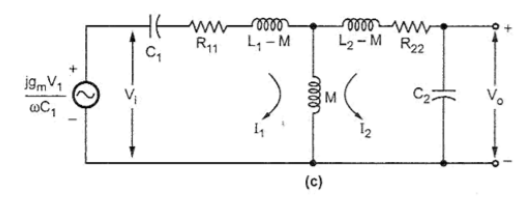 |
Fig 26 Equivalent Circuit for Double Tuned Amplifier
Rp = -
R11 =  + R1
+ R1
R12 =  + R2
+ R2
In simplified circuit the current source is replaced by voltage source which is in series with C1.
Q = 
The Q factor for both the tank circuits will be
Q1 = 
Q2 = 
The Q factor is kept same for both the circuits.
 =
=  =
= 
The output voltage from above figure will be
Vo = - I2
I2
For the above circuit find the value of I2 in terms of V1. The gain will be
AV =  [
[ ]
]
Frequency Response
The coupling between the two tuned circuits determines the frequency response. When there is current carrying coil in the magnetic field emf is induced. In this case the emf is induced in the secondary coil due to the primary coil because of mutual induction.
When the coils are spaced apart, the flux linkages of primary coil L1 will not link the secondary coil L2. At this condition, the coils are said to have Loose coupling. The resistance reflected from the secondary coil at this condition is small and the resonance curve will be sharp and the circuit Q is high as shown in the figure below.
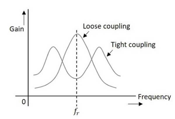 |
Fig 27 Frequency Response
On the other hand, when the primary and secondary coils are brought close together, they have Tight coupling. Under such conditions, the reflected resistance will be large and the circuit Q is lower. Two positions of gain maxima, one above and the other below the resonant frequency are obtained.
The bandwidth is given by
BW =  (f2-f1)
The 3db bandwidth is given by = 3.1fr/Q
Staggered Tuned Amplifier
As we have seen that the double tuned amplifier has flat top and steep sides at 3db bandwidth. SO, in order to rectify this problem two single tuned cascade amplifiers are used and their resonant frequencies are so adjusted that they are separated by an amount equal to the bandwidth of each stage. This allows the staggered tuned amplifier to provide flat and wideband characteristics. The bandwidth is increased in this type of amplifiers.
 |
Fig 28 Response of individual stages Fig 29 Overall response of staggered pair
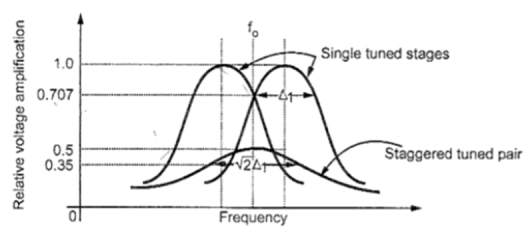 |
Fig 30 Response of individually tuned and staggered tuned pair
The overall gain will be given as
  
 
|
Key takeaway
Tunned amplifiers provided high gain. This is so because a resonant circuit as a load offers high impedance and gain of transistor is dependent on load impedance. Tuned amplifiers are basically designed for narrow bandwidth frequency signal. The resonance frequency of a tuned circuit
Reference:
1 “Electronic Devices and Circuit Theory”, Boylestad and Nashelsky, PEARSON
PUBLICATION.
2 “Electronic devices and circuits”, Salivahanan, Suresh Kumar, Vallavaraj,
TMH, 1999
3 “Integrated Electronics, Analog and Digital Circuits and Systems”, J. Millman
And Halkias, TMH, 2000
4 “Micro Electronic Circuits”, Sedra and Smith, Oxford University Press, 2000
5 “Electronic Devices and Circuits”, David A Bell, Oxford University Press, 2000