Unit 3
DSBSC
DSBFC (Double Side Band Full Wave Carrier)
Time-Domain Representation
Let the modulating signal be,
m(t)=Am cos(2πfmt ) --------------(1)
And the carrier signal be,
c(t)=Ac cos(2πfct)c(t) ---------------(2)
Where, Am and Ac are the amplitude of the modulating signal and the carrier signal respectively.
Fm and fc are the frequency of the modulating signal and the carrier signal respectively.
Then, the equation of Amplitude Modulated wave will be
s(t)=[Ac+ Am cos(2πfmt)] cos(2πfct) -------------------------- (3)
s(t) = [ Ac cos(2πfct) + Ac Am cos(2πfmt) . Cos(2πfct) ] ---------(4)
s(t) = Ac[1 + Am/Ac cos(2πfmt)] cos(2πfct) ----------- (5)
Here the modulation index µ = Am/Ac.
s(t) = Ac[1 + µ cos(2πfmt)] cos(2πfct) -------------- (6)
Modulation index
Let Amax and Amin be the maximum and minimum amplitudes of the modulated wave.
We will get the maximum amplitude of the modulated wave, when cos(2πfmt)
Is 1.
That is Amax=Ac + Am
We will get the minimum amplitude of the modulated wave, when cos(2πfmt)
Is -1.
That is Amin = Ac - Am
Amax + Amin = Ac + Am + Ac –Am = 2Ac
Ac = Amax + Amin/2
Similarly Amax – Amin = Ac + Am – Ac +Am = 2Am
Am = Amax – Amin /2
Therefore
µ = Amax + Amin
Amax - Amin
Bandwidth:
Bandwidth is the difference between the highest and lowest frequencies of the signal.
BW = fmax – fmin
s(t) = Ac[1+ μcos(2πfmt)] cos(2πfct)
s(t) = Ac cos(2πfct) + Ac μcos(2πfmt) cos(2πfct)
s(t) = Ac cos(2πfct) + Ac μ/2 cos 2π (fc + fm)t + Ac μ/2 cos 2π (fc - fm)t
Hence, the amplitude modulated wave has three frequencies.
- Carrier frequency fc
- Upper sideband frequency fc+fm
- And lower sideband frequency fc−fm
Here, fmax=fc+fm and fmin=fc−fm
BW=fc+fm−(fc−fm)
BW=fc+fm−(fc−fm)
BW=2fm
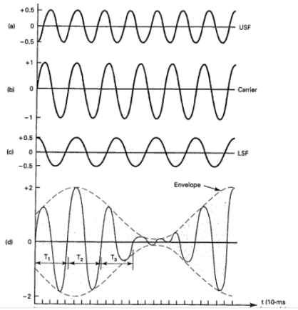
Fig.1: DSBFC
Power Calculation of AM
Consider the following equation of amplitude modulated wave.
s(t)=Ac cos(2πfct)+Acμ 2 cos[2π(fc+fm)t]+ Acμ 2cos[2π(fc−fm)t] -------(1)
Power of AM wave is equal to the sum of powers of carrier, upper sideband, and lower sideband frequency components.
Pt=Pc+ PUSB+ PLSB
We know that the standard formula for power is
P = vrms 2 / R = (vm /  ) 2 /2
Where,
Vrms is the rms value of cos signal.
Vm is the peak value of cos signal.
The powers of the carrier, the upper and lower sideband is given by
Carrier power
Pc=(Ac/√2)2/R=Ac2/2R
Upper sideband power
PUSB=(Acμ/2√2)2/R= Ac2 μ2/ 8R
Similarly, for lower sideband power same as that of the upper side band power.
PLSB=(Acμ/2√2)2 /R
PLSB=Ac2μ2/R
Now, let us add these three powers in order to get the power of AM wave.
Pt=Ac2 /2R+Ac2μ2 /8R+Ac2μ2/8R
Pt= Ac2 /2R[ 1+μ2 /4+μ2 /4]
Pt=Pc ( 1+ μ 2/2 )
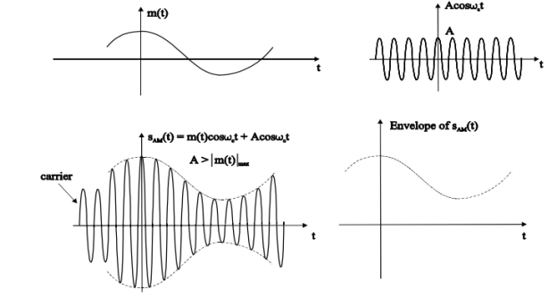
Fig.2: DSBFC
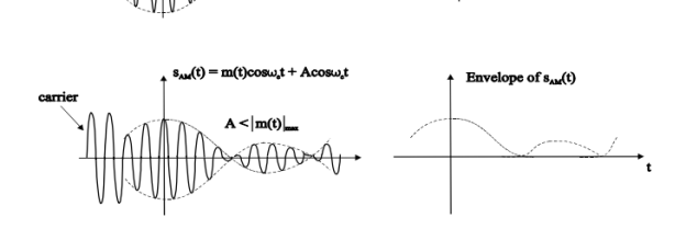
Fig.3: DSBFC
Problems
A modulating signal m(t)=10cos(2π×103t)m(t) is amplitude modulated with a carrier signal c(t)=50cos(2π×105t). Find the modulation index, the carrier power, and the power required for transmitting AM wave.
Solution
Given, the equation of modulating signal as
m(t)=10 cos(2π×103t) m(t)
We know the standard equation of modulating signal as
m(t)=Am cos(2πfmt) m(t)
By comparing the above two equations, we will get
Am=10 volts
And Frequency of modulating signal as
Fm=103Hz=1KHz
Given, the equation of carrier signal is
c(t)=50 cos(2π×105t))
The standard equation of carrier signal is
c(t)=Ac cos(2πfct) c(t)
By comparing these two equations, we will get
Amplitude of carrier signal as Ac=50 volts
And Frequency of carrier signal as fc=105Hz=100KHz
We know the formula for modulation index as
μ=Am/Ac
μ=10/50=0.2
Therefore, the value of modulation index is 0.2 and percentage of modulation is 20%.
The formula for Carrier power, Pc
Pc=Ac2 /2R
Assume R=1ΩR=1Ω and substitute Ac value in the above formula.
Pc=(50)2/2(1)=1250W
Therefore, the Carrier power, Pc is 1250 watts.
We know the formula for power required for transmitting AM wave is
Pt=Pc(1+μ2/2)
Pt=1250(1+(0.2)22)=1275W
Therefore, the power required for transmitting AM wave is 1275 watts.
Key Takeaways:
- Power of AM wave is equal to the sum of powers of carrier, upper sideband, and lower sideband frequency components.
Pt=Pc+ PUSB+ PLSB
2. Bandwidth is the difference between the highest and lowest frequencies of the signal.
BW = fmax – fmin
3. Modulation index is given by µ = Amax + Amin
Amax - Amin
DSBSC (Double Side Band Suppressed Carrier)
In DSBC modulation, the modulated wave consists of only the upper and lower side bands. Transmitted power is saved through the suppression of the carrier wave, but the channel bandwidth requirement is the same.
DSBSC modulators make use of the multiplying action in which the modulating signal multiplies the carrier wave. In this system, the carrier component is eliminated and both upper and lower side bands are transmitted. As the carrier component is suppressed, the power required for transmission is less than that of AM.
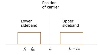
Fig.4: Position of carrier
Carrier is suppressed and base band is allowed for transmission.
If m(t) = Am cos(2πfmt) is the modulating signal and c(t) = Ac cos(2πfct) is the carrier signal then DSBSC wave s(t) is given by
s(t) = c(t) m(t) ------------------- (1)
s(t) =Am cos(2πfmt) Ac cos(2πfct) -------- (2)
s(t) = Am Ac cos(2πfmt) cos(2πfct) ------- (3)
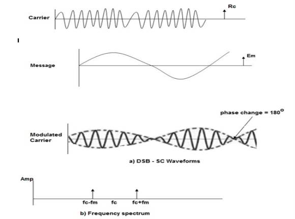
Fig.5: DSBSC
The figure shows the waveform and the frequency spectrum.
The envelope of a DSBSC modulated signal is therefore different from the message signal and the Fourier transform of s(t) is given by
S(f) = Ac/2[ M(f-fc) + M(f + fc)]
When base band signal m(t) is limited to interval –W<fc<W we find the spectrum S(f) of the DSBSC wave s(t) as shown in the figure. We see that there is a change in the scaling factor , the modulation process translates the spectrum of the base band signal by fc. The transmission bandwidth is same as AM.
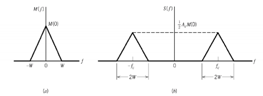
Fig.6: DSBSC transmission bandwidth
Bandwidth of DSBSC Wave
We know the formula for bandwidth (BW) is
BW=fmax−fmin
Consider the equation of DSBSC modulated wave.
s(t)=AmAccos(2πfmt)cos(2πfct)s(t)
s(t)=AmAc2cos[2π(fc+fm)t]+AmAc2cos[2π(fc−fm)t]
The DSBSC modulated wave has only two frequencies. So, the maximum and minimum frequencies are fc+ fm and fc− fm respectively.
i.e.,fmax=fc+fm and fmin=fc−fm
BW=fc+fm−(fc−fm)
BW = 2fm
Thus, the bandwidth of DSBSC wave is same as that of AM wave and it is equal to twice the frequency of the modulating signal.
Power of DSBSC Wave
Consider the following equation of DSBSC modulated wave.
s(t)=AmAc2cos[2π(fc+fm)t]+AmAc2cos[2π(fc−fm)t]
Power of DSBSC wave is equal to the sum of powers of upper sideband and lower sideband frequency components.
Pt=PUSB+PLSB
We know the standard formula for power of cos signal is
P=vrms2 /R=(vm√2)2 /R
First, let us find the powers of upper sideband and lower sideband one by one.
Upper sideband power
PUSB=(AmAc/2√2)2/R=Am2Ac2 / 8R
Similarly, we will get the lower sideband power same as that of upper sideband power.
PLSB=Am2Ac2/8R
Now, let us add these two sideband powers in order to get the power of DSBSC wave.
Pt=Am2Ac2 /8R+Am2Ac2/8R
Pt=Am2Ac2 /4R
Therefore, the power required for transmitting DSBSC wave is equal to the power of both the sidebands.
Generation of DSBSC Waves:
Balanced Modulator (Product Modulator)
A balanced modulator consists of two standard amplitude modulators arranged in a balanced configuration so as to suppress the carrier wave as shown in the following block diagram. It is assumed that the AM modulators are identical, except for the sign reversal of the modulating wave applied to the input of one of them. Thus, the output of the two modulators may be expressed as,
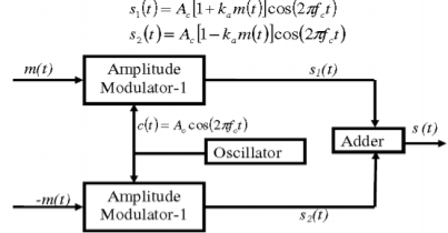
Fig.7: Balanced Modulator
Subtracting s2(t) from s1(t) we get
s(t) = s1(t) – s2(t)
s(t) = 2 ka m(t) cos(2πfct)
Hence, except for the scaling factor 2ka, the balanced modulator output is equal to the product of the modulating wave and the carrier.
Ring Modulator

Fig.8: Ring Modulator
Operation
- In this diagram, the four diodes D1,D2,D3 and D4 are connected in the ring structure. Hence, this modulator is called as the ring modulator.
- Two center tapped transformers are used in this diagram. The message signal m(t) is applied to the input transformer, whereas, the carrier signals c(t) is applied between the two center tapped transformers.
- During the positive half cycle of the carrier signal, the diodes D1 and D3 are switched ON and the other two diodes D2 and D4 are switched OFF.
- In this case, the message signal is multiplied by +1.
- During the negative half cycle of the carrier signal, the diodes D2 and D4 are switched ON and the other two diodes D1 and D3 are switched OFF.
- In this case, the message signal is multiplied by -1. This results in 1800 phase shift in the resulting DSBSC wave.
From the above analysis, we can say that the four diodes D1, D2, D3 and D4 are controlled by the carrier signal.
If the carrier is a square wave, then the Fourier series representation of c(t) is given by
c(t) = 4 / π  n-1 / 2n -1 cos[2πfct(2n−1)]
We will get DSBSC wave s(t) which is just the product of the carrier signal c(t)) and the message signal m(t) i.e.,
s(t) = 4 / π  n-1 / 2n -1 cos[2πfct(2n−1)] m(t)
The ring modulator.
DSBSC modulators are known as product modulators as they produce the output, which is the product of two input signals.
Balanced Modulator using Non-linear resistance
- The DSBSC generation using balanced modulator based on nonlinear resistance characteristics of diode is shown in the figure below.
- The diode in the balanced modulator use the nonlinear resistance property for producing modulated signals.
- Carrier voltage is applied in phase at both the diodes, while modulating voltage appears 180° out of phase at the diode inputs as they are at opposite ends of a center- tapped transformer.
- The modulated output currents of the two diodes are combined in the center tapped primary of the output transformer, which then gets subtracted.
- The output of the balanced modulator contains two sidebands and sum of the harmonic components.
As indicated in the Figure, the input voltage at diode D1 is vc+vm and input voltage at diode D2 is vc−vm.

Fig.9: Balanced Modulator using Non-linear resistance
The primary current of the output transformer is i1=id1−id2.
Where,
Id1=a+ b(vc+vm)+ c(vc+vm)2
Id2=a+ b(vc−vm)+c(vc−vm)2
Thus, we get,
i1= id1−id2=2bvm+4cvmvc
The modulating and carrier voltage are represented as,
Vm=Vmsinωmt and vc=Vcsinωct
Substituting for vm and vc and simplifying, we get,
i1=2bVmsinωmt+4cmVc/2cos(ωc−ωm)t−4cmVc/2cos(ωc+ωm)t
The output voltage v0 is proportional to primary current i1 and assume constant of proportionality as α, which can be expressed as,
v0=αi1=2αbVmsinωmt+4αcmVc/2cos(ωc−ωm)t−4αcmVc/2cos(ωc+ωm)t
Let P=2αbVmP and Q=2αcmVc2.
Thus we have,
v0=Psinωmt+2Qcos(ωc−ωm)t−2Qcos(ωc+ωm)t
The above equation shows that carrier has been cancelled out , leaving only two
Sidebands and the modulating frequencies from the output is eliminated by the tuning of the output transformer, which results in the below equation of the generated DSBSC wave.
v0=2Qcos(ωc−ωm)t−2Qcos(ωc+ωm)t
Switching Modulator
.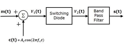
Fig.10 Switching Modulator
Switching modulator is similar to the square law modulator. The only difference is that in the square law modulator, the diode is operated in a non-linear mode, whereas, in the switching modulator, the diode has to operate as an ideal switch.
Let the modulating and carrier signals be denoted as m(t) and c(t)=Accos(2πfct). These two signals are applied as inputs to the summer (adder) block. Summer block produces an output, which is the addition of modulating and carrier signals. Mathematically, we can write it as
V1(t)=m(t)+c(t)=m(t)+Accos(2πfct)
This signal V1(t) is applied as an input of diode.
Assume, the magnitude of the modulating signal is very small when compared to the amplitude of carrier signal Ac. So, the diode’s ON and OFF action is controlled by carrier signal c(t). This means, the diode will be forward biased when c(t)>0 and it will be reverse biased when c(t)<0.
Therefore, the output of the diode is
V2(t)={V1(t)0 if c(t)>0
0 c(t) <0
We can approximate this as
V2(t)=V1(t)x(t)
Where, x(t) is a periodic pulse train with time period T=1fc

The Fourier series representation of this periodic pulse train is
x(t)=1/ 2+2π  n -1 / 2n-1 cos( 2π(2n-1) fc(t))---------------------(1)
= ½ + 2/π cos(2πfct) -2 / 3 π cos(6πfct)+ ………… ----------------(2)
Substituting V1(t) and x(t) we get
V2(t) = [m(t) + Ac cos(2πfct) ] [½ + 2/π cos(2πfct) -2 / 3 π cos(6πfct)+ …………]---------------------------------------(3)
V2(t) = Ac/2 (1+ 4/πAc)m(t) cos(2πfct) + m(t)/2 + 2Ac/π cos (2πfct)- 2m(t)/3π cos(6 πfct)- 2A/3π cos(2πfct) cos(6πfct) + ………………………….
The 1st term of the above equation represents the desired AM wave and the remaining terms are unwanted terms. Thus, with the help of band pass filter, we can pass only AM wave and eliminate the remaining terms.
Therefore, the output of switching modulator is
s(t)=Ac2(1+(4π/Ac)m(t))cos(2πfct)
We know the standard equation of AM wave is
s(t)=Ac[1+kam(t)]cos(2πfct)s(t)
Where, ka is the amplitude sensitivity.
By comparing the output of the switching modulator with the standard equation of AM wave, we will get the scaling factor as 0.5 and amplitude sensitivity ka as 4π/Ac.
SSB-SC
The process of suppressing one of the sidebands along with the carrier and transmitting a single sideband is called as Single Sideband Suppressed Carrier system or simply SSBSC. It is plotted as shown in the following figure.
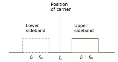
Fig.11 SSB
Carrier and sideband are suppressed and single sideband is allowed for transmission.
Let us consider the
Modulating signal
m(t)=Amcos(2πfmt)
Carrier signal
c(t)=Accos(2πfct)
Mathematically, we can represent the equation of SSB-SC wave as
s(t)=AmAc2cos[2π(fc+fm)t] for the upper sideband
Or
s(t)= AmAc2cos[2π(fc−fm)t] for the lower sideband
Bandwidth of SSB-SC Wave
We know that the DSB-SC modulated wave contains two sidebands and its bandwidth is 2fm. Since the SSB-SC modulated wave contains only one sideband, its bandwidth is half of the bandwidth of DSBSC modulated wave.
i.e., Bandwidth of SSBSC modulated wave =2fm/2=fm
Therefore, the bandwidth of SSB-SC modulated wave is fm and it is equal to the frequency of the modulating signal.
Power Calculations of SSB-SC Wave
Consider the following equation of SSBSC modulated wave.
s(t)=AmAc/2 cos[2π(fc+fm)t] for the upper sideband
Or
s(t)=AmAc/2 cos[2π(fc−fm)t] for the lower sideband
Power of SSB-SC wave is equal to the power of any one sideband frequency components.
Pt=PUSB=PLSB
We know power
P=vrms2 / R
=(vm/√2)2 / R
In this case, the power of the upper sideband is
PUSB=(AmAc/2√2)2 / R = Am2Ac2 /8R.
Similarly, for lower sideband power.
PLSB=Am2Ac2 / 8R
Therefore, the power of SSB-SC wave is
Pt=Am2Ac2 / 8R
Advantages
- Bandwidth or spectrum space occupied is lesser than AM and DSBSC waves.
- Transmission of more number of signals is allowed.
- Power is saved.
- High power signal can be transmitted.
- Less amount of noise is present.
- Signal fading is less likely to occur.
Disadvantages
- The generation and detection of SSBSC wave is a complex process.
- The quality of the signal gets affected unless the SSB transmitter and receiver have an excellent frequency stability.
Applications
- Power saving requirements and low bandwidth requirements.
- In land, air, and maritime mobile communications.
- Point-to-point communications.
- Radio communications.
- Television, telemetry, and radar communications.
- Military communications, such as amateur radio, etc.
Generation of SSB-SC
We can generate SSBSC wave using the following two methods.
- Frequency discrimination method
- Phase discrimination method
Frequency Discrimination Method
In this method the DSB signal is passed through band pass filter to generate SSB signal.
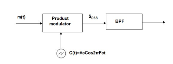
Fig.12 Frequency Discrimination method
The center frequency of the band pass signal decides whether USB or LSB signal is generated.
Suppose we want to transmit USB then using band pass filter with center frequency fc + w/2 we obtain the desired result as shown in the figure.
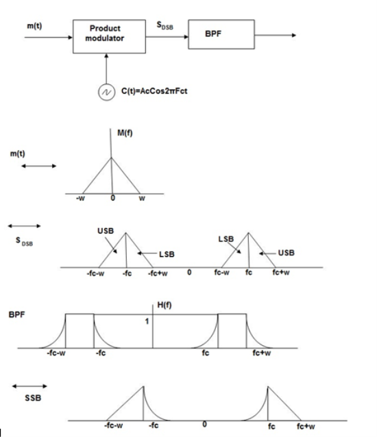
Fig.13: Resultant output
Phase Discriminated Method:
Consider the following block diagram of SSB-SC modulator using phase discrimination method.
.
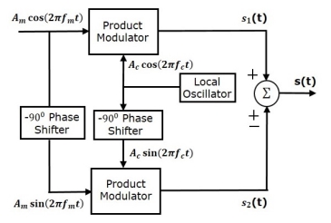
Fig.14 Phase Discriminated Method
- It consists of two product modulators, two −900 phase shifters, one local oscillator and one summer block.
- The product modulator produces an output, which is the product of two inputs.
- The −900 phase shifter produces an output, which has a phase lag of −900 with respect to the input.
- The local oscillator is used to generate the carrier signal.
- Summer block produces an output, which is either the sum of two inputs or the difference of two inputs based on the polarity of inputs.
The modulating signal
m(t) = Amcos(2πfmt) -----------------(1)
The carrier signal
c(t) = Accos(2πfct) -----------------------(2)
Which are directly applied as inputs to the upper product modulator. So, the upper product
Modulator produces an output, which is the product of these two inputs.
The output of upper product modulator is
s1(t)=AmAc cos(2πfmt)cos(2πfct) --------------------(3)
s1(t)=AmAc/2{cos[2π(fc+fm)t]+cos[2π(fc−fm)t]} -----------(4)
The modulating signal Am cos(2πfmt) and the carrier signal Ac cos(2πfct) are phase shifted by −900 before applying as inputs to the lower product modulator. So, the lower product modulator produces an output, which is the product of these two inputs.
The output of lower product modulator is
s2(t)=AmAc cos(2πfmt−900)cos(2πfct−900) ---------------(5)
s2(t)=AmAc sin(2πfmt) sin(2πfct) -------------------(6)
s2(t)=AmAc/2{cos[2π(fc−fm)t]−cos[2π(fc+fm)t]} ----------(7)
Add s1(t) and s2(t) in order to get the SSB-SC modulated wave s(t) having a lower sideband.
s(t)=AmAc/2{cos[2π(fc+fm)t]+cos[2π(fc−fm)t]}+AmAc/2{cos[2π(fc−fm)t]−cos[2π(fc+fm)t]} ----------------------------------(8)
s(t)=AmAc cos[2π(fc−fm)t] ------------------------(9)
Subtract s2(t) from s1(t) in order to get the SSBSC modulated wave s(t) having a upper sideband.
s(t)=AmAc/2{cos[2π(fc+fm)t]+cos[2π(fc−fm)t]}−AmAc/2{cos[2π(fc−fm)t]−cos[2π(fc+fm)t]} ---------------------------------------------------------(10)
s(t)=AmAc cos[2π(fc+fm)t] --------------------------(11)
Hence, by properly choosing the polarities of inputs at summer block, we will get SSB-SC wave having a upper sideband or a lower sideband.
Key Takeaways:
- We can generate SSBSC wave using the following two methods.
- Frequency discrimination method
- Phase discrimination method
2. The power of SSB-SC wave is Pt=Am2Ac2 / 8R
3. The process of suppressing one of the sidebands along with the carrier and transmitting a single sideband is called as Single Sideband Suppressed Carrier system or simply SSBSC.
4. The power of DSB-SC wave is Pt=Am2Ac2 /4R
5. In DSBC modulation, the modulated wave consists of only the upper and lower side bands. Transmitted power is saved through the suppression of the carrier wave, but the channel bandwidth requirement is the same.
De- modulation of double side band with carrier in coherent detector or envelope detector
The message signal m(t) can be recovered from a DSB-SC modulated wave s(t) with the help of a locally generated sine wave and then passing through a low-pass filter.
The local oscillator’s output is synchronised, in both frequency and phase with the carrier wave c(t) and is used in the product modulator to generate s(t).
This method of demodulation is called “Coherent Detection”.
Now, the pass-band of the low-pass filter is extended over the entire message spectrum and must satisfy two requirements:
1. Cutoff frequency : ωB
2. Transmission band : ωB ≤ ω ≤ 2 ωc −ωB
Thus the overall output is given by

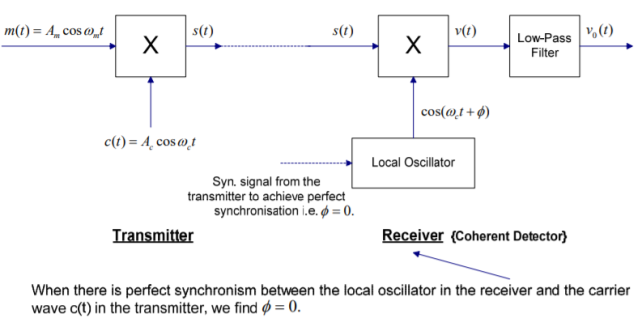
Fig.15 Envelop Detector
Peak diode detector
Rectifier circuit gives average value of input signal; but practically peak value of input signal is required.
This can be achieved by peak detector circuit.
The figure shows a simple peak detector circuit using diode and capacitor.
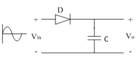
Fig.16 Peak diode Detector
In the positive half cycle, diode D is forward biased and capacitor C begins to charge. When input voltage reaches its peak value, capacitor gets charged to positive peak value.
In negative half cycle, as input voltage decreases, diode D becomes reverse biased and capacitor remains isolated and holds the peak value of previous cycle.
Hence called as peak detector.
But practically, output is taken across some load RL, hence as input voltage decreases capacitor discharges through load RL.
To avoid this, RL is kept at a very large value so that capacitor discharges slowly hence almost holds the charge. Whatever charge it lost through RL is again achieved back in next half cycle.
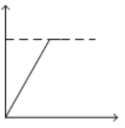
Fig.17 Output
Here, the diode D is acts as an instant switch, so supply gets loaded.
To avoid loading effect while charging capacitor, we use op-amp.
Op-amp is placed between input and diode D so loading is avoided as shown below,

Fig.18 Peak Detector
Coherent or synchronous detection of DSBSC
The process of extracting an original message signal from DSBSC wave is known as detection or demodulation of DSBSC. The following detectors are used for demodulating DSBSC wave.
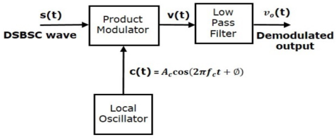
Fig.19 Coherent Detector
Here, the message signal can be obtained from DSBSC wave by multiplying it with a carrier having the same frequency and the phase in the product modulator. The signal is then passed through a Low Pass Filter and the desired message signal is obtained.
Let the DSBSC wave be
s(t)=Ac cos(2πfct) m(t)s(t)
=Ac cos(2πfct) m(t)
The output of the local oscillator is
c(t)=Ac cos(2πfct+ϕ) c(t)=Ac cos(2πfct+ϕ)
Where, ϕ is the phase difference between the oscillator signal and the carrier signal, that is used for DSBSC modulation.
From the figure, we can write the output of product modulator as
v(t)=s(t)c(t)v(t)=s(t)c(t)
Substitute, s(t) and c(t) values in the above equation.
⇒v(t)=Accos(2πfct)m(t)Accos(2πfct+ϕ)⇒v(t)=Accos(2πfct)m(t)Accos(2πfct+ϕ)
=Ac cos(2πfct)cos(2πfct+ϕ)m(t)=Ac cos(2πfct)cos(2πfct+ϕ)m(t)
=Ac [cos(4πfct+ϕ)+cosϕ]m(t)=Ac [cos(4πfct+ϕ)+cosϕ]m(t)
v(t)=Ac cosϕm(t)+Ac cos(4πfct+ϕ)m(t)v(t)
=Ac cosϕm(t)+Ac cos(4πfct+ϕ)m(t)
Here, the first term is the scaled version of the message signal. It can be obtained by passing the above signal through a low pass filter.
Therefore, the output of low pass filter is
v0t=Ac cosϕ m(t) v(t)=Ac cosϕm(t)
The demodulated signal amplitude will be maximum, when ϕ=0. Therefore, the local oscillator signal and the carrier signal should be in phase, i.e., there should not be any phase difference between these two signals.
The demodulated signal amplitude remains zero, when ϕ=±90.
This effect is known as quadrature null effect.
Coherent or synchronous detection of Single side band with suppressed carrier
1. Synchronous Detector
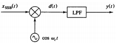
Fig.20 Synchronous Detector
2. Phase shift detector
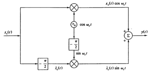
Fig.21 Phase shift detector
References:
- “Electronic communication system”, by Kennedy, TMH
- “Communication system”, by haykin wiley
- “Communication system”, by bruce carison, TMH
- “Modern digital and analog communication”, B.P. LATHI, Oxford