UNIT 1
PN Junction Diode
P-N JUNCTION
When a semi-conductor is doped such that half the portion is doped with the trivalent impurity (Al, Ar, Bi) and the other half is doped with pentavalent impurity (B, P) then the junction formed is known as PN junction.

Its symbol is

At normal condition, the holes from P region diffuse into N region and electrons from N region diffuse in P region.
A thin layer of positive ion is formed in the N region and negative ions in the P region near the junction are formed.
This thin layer that is formed is known as depletion layer.
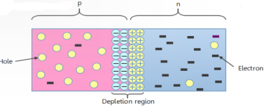
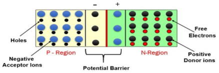
The potential barrier in the PN-junction diode is the barrier in which the charge requires additional force for crossing the depletion region.
Here, the depletion region acts as a barrier and opposes the flow of charge carrier.
Depending on the type of material used, the value of barrier potential lies between 0.3 – 0.7V.
Forward Biased P-N Junction
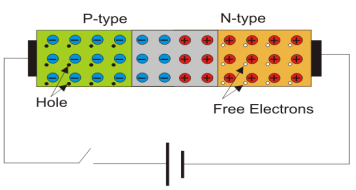
When p-type region is connected with the positive terminal and n-type region with the negative terminal of the voltage source, then the junction is said to be forward biased.
At this condition, due to the attraction of cathode, electrons create covalent bond in p-type material and are attracted towards the terminal.
Hence, numbers of covalent bonds are broken and electrons moves towards the positive terminal increasing the concentration of electrons in the crystal nearer to the terminal and these electrons recombine with holes here.
In this way, the number of holes increases in the p-type region away from the junction, and it is reduced in the portion of p-type region nearer to the terminal.
Due to the higher concentration of holes adjacent to negative impurity ions layer the electrons of negative ions come out and recombine with those holes and create new holes in the layer.
Consequently, the width of this negative ions layer is reduced and finally this layer vanishes.
Reverse Biased PN Junction
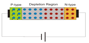
When positive terminal is connected to the n-type region and the negative terminal is connected to the p-type region then the pn junction is said to be in reverse biased condition.
When no voltage applied across the p n junction, the potential developed across the junction is 0.3 volts at 25oC for germanium and 0.7 volts at 25oC for silicon p n junction.
The polarity of this potential barrier is same as the polarity of voltage source applied during reverse biased condition.
Now if reverse biased voltage is increased the barrier potential developed also increases. Hence, the pn junction widens.
The free electrons of the n-type region are attracted towards positive terminal of the source because of that more positive impurity ions are created in the depletion layer which makes the layer thicker.
At the same time, electrons are injected in the p-type region. Due to the positive potential of the n-type region the electrons are drifted towards the junction and combine with holes and create more positive impurity ions in the layer.
Key Takeaways:
- The free electrons from the negative terminal of the battery continue to pour into the n-region while the free electrons in the n-region move towards the junction.
- The electrons travel through the n-region as free electrons hence, current in n-region is by free electrons.
- When these electrons reach the junction, they combine with holes and become valence electrons.
- As valence electron, they move through the holes in the p-region, hence, current in the p-region is by holes.
- When these valence electrons reach the left end of the crystal, they flow into the positive terminal of the battery.
In the reverse bias, the voltage increases in the reverse direction but no current across the p-n junction due to the majority carriers. Only a very small leakage current flows. But at a certain reverse voltage p-n junction breaks in conduction. It is only due to the minority carriers. This amount of voltage is sufficient for these minority carriers to break the depletion region. At this moment sharp current flows through the junction. This breakdown of voltage is of two types.
- Avalanche Breakdown: It is not sharp, rather it is an inclined linear graph i.e. after break down small increase in reverse voltage causes more sharp current.
- Zener Breakdown: It is sharp and there is no need to increase reverse bias voltage to get more current, because current already flows sharply.
In the forward bias, the operational region is in the first quadrant.
The threshold voltage for Germanium is 0.3 V and for Silicon is 0.7 V.
Beyond this, the graph goes upward in a non linear manner.
This graph is for the dynamic Resistance of the junction in the forward bias.
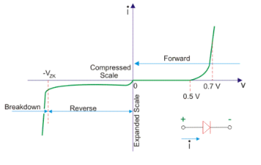
It is the minimum amount of voltage which is required to operate components like for silicon diode it is 0.7 V while for Germanium Diode its 0.3 V
The ideal diode or perfect diode is a two terminal device, which allows the electric current without any loss in forward bias and completely blocks the electric current with infinite loss in reverse bias condition.
Ideal diodes actually do not exist. However, the V-I characteristics of ideal diodes is used to study the diode circuits.
It is not possible to design an ideal diode,however, a well-designed diode behaves almost like a perfect diode or ideal diode.
Ideal diode symbol
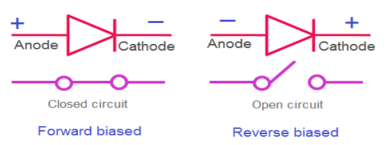
The Forward and reverse characteristics
If the forward voltage (VF) (p terminal is connected to p-side and n terminal is connected to n-side) applied on the diode is equal to zero or greater than zero, the forward electric current (IF) in the ideal diode increases infinitely.
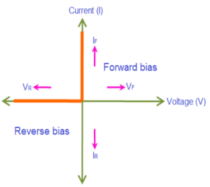
On the other hand, if the reverse voltage (VR) (p terminal is connected to n-side and n-terminal is connected to p-side) applied on the diode is less than zero, no forward electric current (IF) and reverse electric current (IR) flows in the ideal diode.
The ability of the material to store electric charge is called capacitance.
The change of capacitance at the depletion region can be defined as the change in electric charge per change in voltage.
CT = dQ / dV
Where,
CT = Transition capacitance
DQ = Change in electric charge
DV = Change in voltage
Transition Capacitance
The amount of capacitance changes with increase in voltage is called transition capacitance.
The transition capacitance is also known as depletion region capacitance, junction capacitance or barrier capacitance. Transition capacitance is denoted as CT.
The transition capacitance can be mathematically written as,
CT = ε A / W
Where,
ε = Permittivity of the semiconductor
A = Area of plates or p-type and n-type regions
W = Width of depletion region
Diffusion capacitance (CD)
It occurs in a forward biased p-n junction diode.
It is also referred as storage capacitance. It is denoted as CD.
Diffusion capacitance is given by,
CD = dQ / dV
Where,
CD = Diffusion capacitance
DQ = Change in number of minority carriers stored outside the depletion region
DV = Change in voltage applied across diode
A zener diode is a special type of device designed to operate in the zener breakdown region.
It acts like normal p-n junction diode under forward bias condition. When forward biased voltage is applied, it allows large amount of electric current and blocks only a small amount.
It is heavily doped than the normal p-n junction diode. Hence, it has very thin depletion region. Hence, allows more electric current than the normal p-n junction diodes.
It allows electric current in the reverse direction if the applied reverse voltage is greater than the zener voltage.
It is always connected in reverse direction because it is specifically designed to work in reverse direction.
Symbol

V-I characteristics

Advantages :
- Power dissipation capacity is very high
- High accuracy
- Small size
- Low cost
Applications :
- It is normally used as voltage reference
- It is used in voltage stabilizers or shunt regulators, in switching operations.
- It is used in clipping and clamping circuits and in various protection circuits.
Avalanche Diode:
An avalanche diode is a special type of semiconductor device designed to operate in reverse breakdown region. Avalanche diodes are used as relief valves (a type of valve used to control the pressure in a system) to protect electrical systems from excess voltages.
Construction
Avalanche diodes are generally made from silicon or other semiconductor materials. The construction of avalanche diode is similar to zener diode but the doping level in avalanche diode differs from zener diode.
Zener diodes are heavily doped. Therefore, the width of depletion region in zener diode is very thin. Because of this thin depletion layer or region, reverse breakdown occurs at lower voltages in zener diode.
On the other hand, avalanche diodes are lightly doped. Therefore, the width of depletion layer in avalanche diode is very wide compared to the zener diode. Because of this wide depletion region, reverse breakdown occurs at higher voltages in avalanche diode. The breakdown voltage of avalanche diode is carefully set by controlling the doping level during manufacture.
Symbol of avalanche diode
The symbol of avalanche and zener diode is same. Avalanche diode consists of two terminals: anode and cathode. The symbol of avalanche diode is shown in below figure.
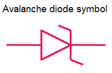
The symbol of avalanche diode is similar to the normal diode but with the bend edges on the vertical bar.
Working:
A normal p-n junction diode allows electric current only in forward direction whereas an avalanche diode allows electric current in both forward and reverse directions. However, avalanche diode is specifically designed to operate in reverse biased condition.
Avalanche diode allows electric current in reverse direction when reverse bias voltage exceeds the breakdown voltage. The point or voltage at which electric current increases suddenly is called breakdown voltage.
When the reverse bias voltage applied to the avalanche diode exceeds the breakdown voltage, a junction breakdown occurs. This junction breakdown is called avalanche breakdown.
When forward bias voltage is applied to the avalanche diode, it works like a normal p-n junction diode by allowing electric current through it.
When reverse bias voltage is applied to the avalanche diode, the free electrons (majority carriers) in the n-type semiconductor and the holes (majority carriers) in the p-type semiconductor are moved away from the junction. As a result, the width of depletion region increases. Therefore, the majority carriers will not carry electric current. However, the minority carriers (free electrons in p-type and holes in n-type) experience a repulsive force from external voltage.
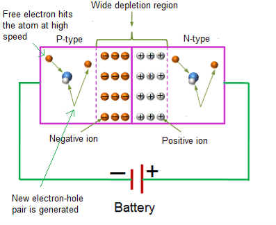
As a result, the minority carriers flow from p-type to n-type and n-type to p-type by carrying the electric current. However, electric current carried by minority carriers is very small. This small electric current carried by minority carriers is called reverse leakage current.
If the reverse bias voltage applied to the avalanche diode is further increased, the minority carriers (free electrons or holes) will gain large amount of energy and accelerated to greater velocities.
The free electrons moving at high speed will collide with the atoms and transfer their energy to the valence electrons.
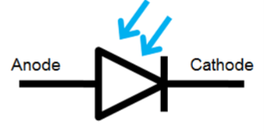
A photodiode is a p-n junction or pin semiconductor device that consumes light energy to generate electric current. It is also sometimes referred as photo-detector, photo-sensor, or light detector.
Photodiodes are specially designed to operate in reverse bias condition. Reverse bias means that the p-side of the photodiode is connected to the negative terminal of the battery and n-side is connected to the positive terminal of the battery.
Photodiode is very sensitive to light so when light or photons falls on the photodiode it easily converts light into electric current. Solar cell is also known as large area photodiode because it converts solar energy or light energy into electric energy.
Symbol
Advantages :
- Low cost
- Small size
- Long lifetime
Applications :
- Compact disc players
- Smoke detectors
- Space applications
- Photodiodes are used in medical applications such as computed tomography, instruments to analyze samples, and pulse oximeters.
Light Emitting Diodes (LEDs) are the most widely used semiconductor diodes.
It emits either visible light or invisible infrared light when forward biased.
It is an optical semiconductor device that emits light when voltage is applied. It converts electrical energy into light energy.
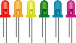
When LED is forward biased, free electrons in the conduction band recombines with the holes in the valence band and releases energy in the form of light.
The process of emitting light in response to the strong electric field or flow of electric current is called electroluminescence.
It works only in forward bias condition. When LED is forward biased, the free electrons from n-side and the holes from p-side are pushed towards the junction.
When free electrons reach the junction or depletion region, some of the free electrons recombine with the holes in the positive ions.

The current flowing through the LED is mathematically written as

Where,
IF = Forward current
VS = Source voltage or supply voltage
VD = Voltage drop across LED
RS = Resistor or current limiting resistor
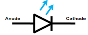
Symbol
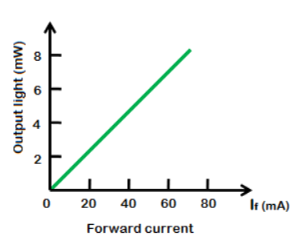
Output characteristics of LED
Advantages :
- LEDs are very cheap and readily available.
- LEDs are light in weight.
- Smaller size.
- LEDs have longer lifetime.
- LEDs operates very fast.
Applications :
- Calculators
- Picture phones
- Traffic signals
- Digital computers
- Multimeters
References:
- “Electronic devices and circuit theory” by Boylestead and Nashelsky, Pearson
- “Electronic principle” by Albert Malvino and Davis J Bates, TMH
- “Integrated Electronics”, By Jacob Millman and Christos Halkias