UNIT 3
BJT Introduction
Bi polar junction transistor (BJT)
It is an electronic device with three terminals namely base, emitter and collector.
It is made of three layers consisting of two n and one p named as npn transistor or one n and two p named as pnp transistor.
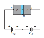

Fig 1 : (a) pnp transistor (b) npn transistor
- The operation is explained by considering the PNP transistor. The operation of NPN transistor varies with a little exchange of roles played by the electrons and holes.
- Now, there is a reduction in the width of the depletion layer due to the applied bias which results in a heavy flow of majority carriers from p to n type material.
- On removing the base emitter bias of pnp transistor we get forward biasing of transistor.
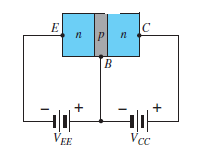
Fig. 2: Forward bias of pnp transistor (Ref. 2)
- Now if the flow of majority carrier is zero then the flow of minority carrier leads to reverse bias condition.
- When both the biasing potentials are applied simultaneously then both the majority and minority carriers start flowing.
- Here the n type material is very small and has less conductivity hence the magnitude of base current is of the order of microamperes
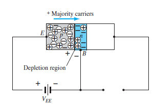
Fig. 3: pnp transistor (Ref. 2)
- Now applying Kirchoff’s law we get
Ie = Ic + Ib
- Hence, the emitter current is sum of the collector current and base current.
- The collector current has two components : the majority (Icm) and minority currents (Ico).
Ic = Icm + Ico
- Ico is known as the leakage current and is measured in micro or nano amperes.
- It is temperature sensitive and can affect the stability of the system with high temperature requirement if not considered properly.
The notation and symbols of pnp and npn transistors are given below:
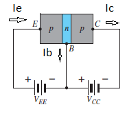
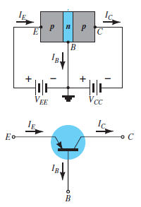
Fig. 4: PNP CB and NPN CB (Ref. 2)
Here the base is common to both the input and output sides of the configuration.
The flow of holes will govern the direction of current.
Hence, Ic = Ib + Ie
Where Ic, Ib, Ie are the collector, base and emitter currents respectively.
The graphical symbol of the PNP common base configuration is
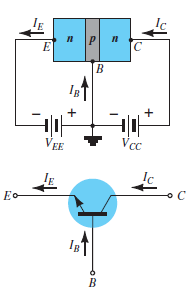
Fig. 5 : PNP common base(Ref. 2)
The arrow in the above symbol shows the direction of emitter current in the device.
Now, to study the behavior of the device we require two characteristics:
Input Characteristic Curve
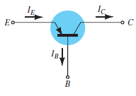
Fig.6: Input Characteristic Curve (Ref. 2)
- It is the relation between the input current IE to the input voltage VBE for various levels of output voltage VCB.
- It is also known as driving point characteristics.
Output Characteristic Curve
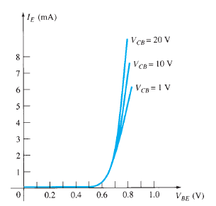
Fig.7 : Output Characteristic Curve (Ref. 2)
- It is the relation between the output current IC to the output voltage VCB for various levels of input current IE.
- It is also known as collector set of characteristics.
- It has three basic regions:
- Active Region
Here, base-emitter junction is forward biased and collector-base junction is reverse biased.
As input current IE increases above zero, output current IC increases to a magnitude equal to IE as determined by the basic transistor current relationship.
So the first approximation determined by the curve is
IC ≈ IE
2. Cut-off Region
It is defined as the region where the collector current IC is equal to 0A.
Here, the base-emitter junction and the collector-base junction both are in reverse bias.
3. Saturation Region
It is the region that lies towards the left of VCB = 0V.
Here, the base-emitter junction and the collector-base junction both are in forward bias.
Common Emitter Configuration
The notation and symbols of npn and pnp transistors are given below:
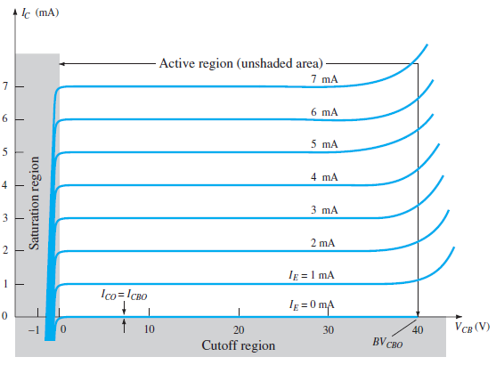
Fig. 8: NPN CE and PNP CE (Ref. 2)
In the above figure all the currents are shown in their actual conventional directions.
The current relation developed earlier is still applicable,
IE = IB + IC
Where IE , IB , IC are the collector, base and emitter currents respectively.
The graphical symbol of the PNP common emitter configuration is
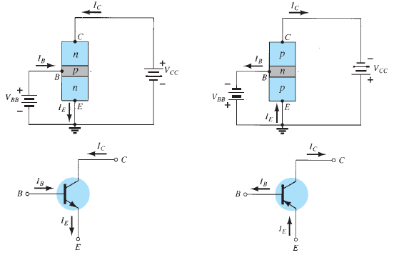
Fig. 9 : PNP common emitter (Ref. 2)
Now, to study the behavior of the device we require two characteristics:
Input Characteristic Curve
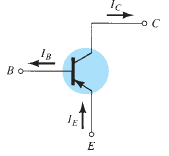
Fig.10: Input Characteristic Curve (Ref. 2)
It is the graph between the input current IB to the input voltage VBE for a range of values of output voltage VCE.
Note that the magnitude IB of is in micro amperes and that of IC is in milli amperes.
Output Characteristic Curve
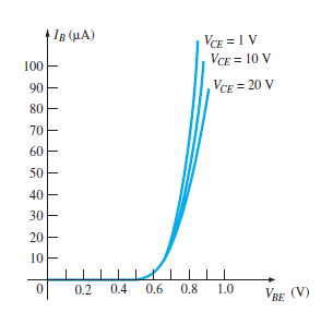
Fig.11: Output Characteristic Curve (Ref. 2)
It is the graph between the output current IC to the output voltage VCE for a range of values of input current IB.
It has three basic regions:
Active Region
- Here, the base-emitter junction is forward biased and collector base junction is reverse biased.
- These are the same conditions that existed in the active region of the common base configuration.
- This can be employed for voltage, current or power amplification.
Cut-off Region
- Here IC is not equal to zero when IB is zero.
- For linear amplification purposes, it is defined as IC = ICEO .
- The region below IB = 0µA is to be avoided for undistorted output signal.
- When the transistor is used as a switch, the condition should be ideally IC = 0mA for a chosen VCE voltage.
Saturation Region
- It is the region that lies towards the left of VCE = 0V.
Common Collector Configuration
The notation and symbols of npn and pnp transistors are given below:
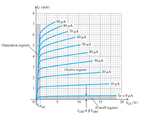
Fig. 12: NPN CC and PNP CC (Ref. 2)
In the above figure all the currents are shown in their actual conventional directions.
It is used for impedence matching purposes as it has high input impedence and low output impedence.
It can be designed using common emitter characteristics.
The output characteristics of common collector is same as that of common emitter configuration for all practical purposes.
The output characteristics are a plot between IE versus VCE for all values of IB.
The input current of common collector is same as that of common emitter configuration.
Here the region of operation will ensure that maximum ratings are not being exceeded and output ratings have minimum distortion.
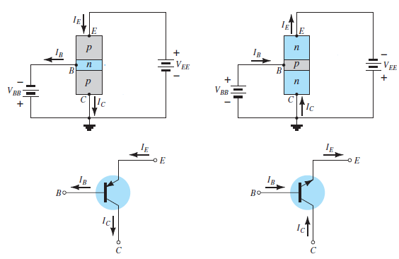
Fig.13: Output Characteristic Curve (Ref. 2)
The characteristics specifying the minimum VCE that can be applied without entering the non-linear region is saturation region.
The maximum power dissipation is given by,
P = VCE . IC
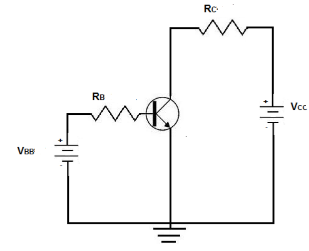
Base bias is the simplest way of biasing a BJT transistor. It ensures that the voltage applied at the base, VBB, is correct, which then supplies this current so that the BJT has enough base current to switch on the transistor.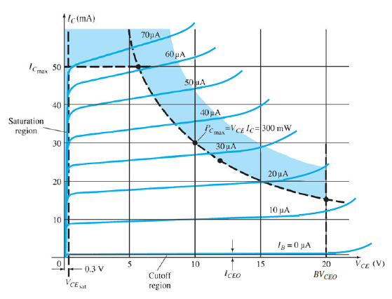
VBB is used to provide sufficient current to turn on the transistor. RB is used to provide the desired value of base current IB. VCC is the collector supply voltage required for a transistor to have sufficient power to operate. This voltage, reverse-biases the transistor, so that the transistor has sufficient power to have an amplified output collector current. The collector resistor, RC provides the desired voltage in the collector circuit
The base current is found by dividing the voltage across resistor RB shown below:
IB= (VBB - VBE)/RB
Since the voltage drop across a silicon junction is 0.7V, the value of VBE=0.7V. Therefore, IB equals:
IB= (VBB - VBE)/RB= (5v - 0.7v)/56kΩ= 76.78µA
The collector current IC can be calculated next:
IC=βdc x IB= 100 x 76.78µA≈ 7.68mA
With IC then known, the collector-emitter voltage, VCE can be calculated.
VCE= VCC - IC x RC= 15v - (7.68mA x 1KΩ)= 7.32v
Base biasing can also be done with a single supply voltage, VCC, omitting VBB. So instead of using VBB in calculations, you use VCC. The result of the calculations remains the same.
Disadvantages:
- βdc of a transistor is one of the most unstable and unpredictable parameters of a transistor.
- βdc is also susceptible to changes due to temperature.
Key Takeaways:
- Base bias ensures that the voltage applied at the base, VBB, is correct, which then supplies this current so that the BJT has enough base current to switch on the transistor.
Emitter feedback bias
When an emitter is added to the base bias circuit, emitter feedback bias is formed.
It is done to make base bias more predictable for negative feedback.
It is used to negate the change in collector current with an opposing change in base current.
When collector current increases, emitter voltage increases.
Hence, base voltage,
VB = VE + VBE
Applying Kirchoff’s voltage law,
-VCC + IB.RB + VBE + IE.RE = 0
Substituting IB = IE / Βdc
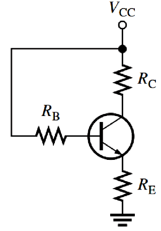
Increase in the base voltage, reduces voltage across RB.
This further reduces the base current and collector current.
Key Takeaways:
- When an emitter is added to the base bias circuit, emitter feedback bias is formed.
- It is done to make base bias more predictable for negative feedback.
Voltage divider bias
In the previous configurations, the bias current and the collector emitter voltage were a function of current gain β of a transistor.
Since β is temperature sensitive, actual value could not be defined .
Hence it is very much desired to develop a bias circuit which is independent of β.
This gives a Voltage divider configuration.
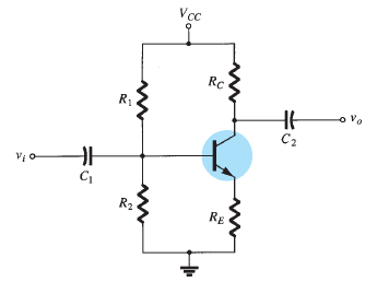
Fig.: Voltage Divider Bias (Ref. 2)
When analysed on exact basis, the sensitivity to changes in β is very small and if circuit parameters are nicely chosen then it can even become independent of β.
IB changes with the change in β but the operating point on the characteristics defined by Ic and Vce remain fixed if proper parameters are employed.
Applying exact analysis, the above circuit is redrawn as,

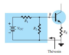
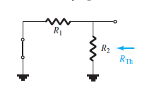
Fig.: Analysis of Voltage Divider circuit (Ref. 2)
The voltage is replaced by a short circuit equivalent (Ref. 2)

Now calculating open circuit thevenin’s voltage and applying voltage divider rule we have (Ref. 2)

Applying kirchoff’s voltage law , (Ref. 2)

Put IE = ( β + 1 ) IB

Once IB is determined then rest of the quantities can be found out (Ref. 2)

The remaining equations for collector, emitter and base voltages are same as obtained for emitter- bias configuration.
Key Takeaways:
- When analysed on exact basis, the sensitivity to changes in β is very small and if circuit parameters are nicely chosen then it can even become independent of β.
- IB changes with the change in β but the operating point on the characteristics defined by Ic and Vce remain fixed if proper parameters are employed.
Numerical
Determine dc bias voltage VCE and current IC for voltage divider configuration. (Ref. 2)
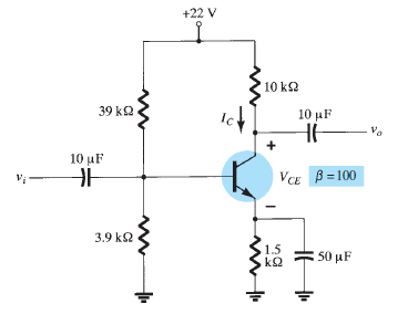
Solution:


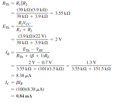

- The load line solution was found by superimposing the actual characteristics on a plot of network equation involving the same network variables.
- It is known as load line analysis as load of network defined the slope of the straight line connecting the points defined by network parameters.
- The smaller the load resistance, the steeper the slope of the network load line.
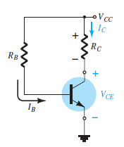
Fig.: DC Load Line (Ref. 2)
- The output equation is given by,

- The characteristic curve is drawn as
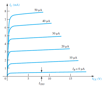
Fig.: DC Load Line characteristic curve (Ref. 2)
- When Ic = 0mA then

- If we choose VCE = 0V then,

Key Takeaways:
- The load line solution was found by superimposing the actual characteristics on a plot of network equation involving the same network variables.
- It is known as load line analysis.
Numerical
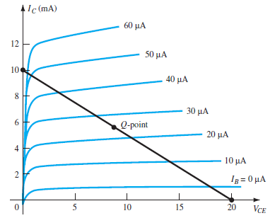
Determine the values of VCC RC and RB of a fixed bias configuration for a given load line and defined Q point.
Solution:
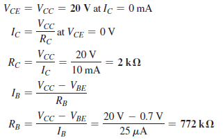
When a line is drawn by joining the saturation and cut off points then such a line is called as Load line.
This line is drawn over the output characteristic curve which contacts at a point called as Operating point.
It is also known as quiescent point or simply Q-point.
The Q-point is selected in such a way that irrespective of AC signal swing, the transistor remains in the active region.
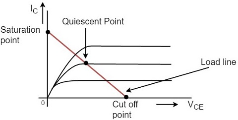
The operating point is not disturbed and remains stable to achieve faithful amplification. Hence the Faithful Amplification is achieved.
Key Takeaways:
- It is also known as quiescent point or simply Q-point.
H parameters of BJT
References:
1 “Electronic devices and circuit theory” by Boylestead and Nashelsky, Pearson
2 “Electronic principle” by Albert Malvino and Davis J Bates, TMH
3 “Integrated Electronics”, By Jacob Millman and Christos Halkias