Unit 4
FET
- An FET is a three-terminal amplifying device.
- Its terminals are source, gate, and drain, which acts respectively like emitter, base, and collector of a normal transistor.
- There are two distinct families of FETs.
- The first is known as ‘junction-gate’ types of FETs or JUGFET or JFET.
- The second family is called ‘insulated-gate’ FETs or Metal Oxide Semiconductor FETs or MOSFET.
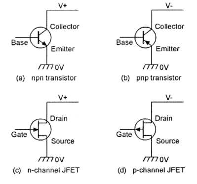
- ‘N-channel’ and ‘p-channel’ are the two versions of both types of FET.
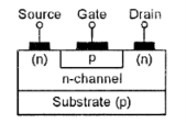
- N-channel FET consists of n-type semiconductor material with a drain terminal and a source terminal at opposite ends.
- A p-type gate is joined in the middle section of the n-type bar, thus forming a p-n junction.
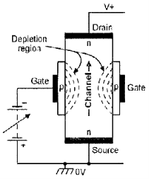
- The drain terminal is connected to a positive supply and the gate is biased at a value that is negative (or equal) to the source voltage, thus reverse-biasing the JFET’s internal p-n junction, and accounting for its very high input impedance.
- When gate = 0V, a current flow from drain to source via a conductive ‘channel’ and the n-type bar is formed.
- When gate = negative , a high resistance region is formed within the junction, thus reduces the magnitude of the drain-to-source current and width of the n-type conduction channel.
- Thus, the basic JFET passes maximum current when its gate bias is zero, and its current is reduced or ‘depleted’ when the gate bias is increased. It is thus known as a ‘depletion-type’ n-channel JFET.
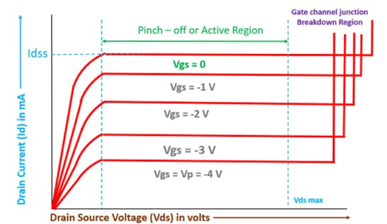
Output Characteristics or Drain Characteristics
- In the absence of external bias: In this case, as there is no voltage between gate and source terminal, thus, the drain current will flow from drain terminal to source terminal. We have already discussed in the working of JFET that majority charge carriers flow from source to drain and as a consequence of which the current flows from drain to source.

2. With external bias: When the external bias is applied to the gate-source terminal, the gate-source terminal becomes reversed bias externally. Obviously, if we are supplying an external voltage, then we can achieve the pinch-off point quite early as compared to the circuit which is not biased.
Transfer Characteristics
The transfer characteristics can be determined by observing different values of drain current with variation in gate-source voltage provided that the drain-source voltage should be constant. The transfer characteristics are just opposite to drain characteristics.

1. Gate Cut Off Voltage
At a fixed drain voltage, the drain current (ID) of a JFET depends on the gate to source voltage (VGS). If the gate to source voltage decreases in n channel JFET, the drain current also gets decreased accordingly.
The relation between gate to source voltage and drain current is given by
2. Shorted Gate Drain Current
When (VGS = 0) and positive drain to source voltage (VDS) is being increased slowly, the drain current gets increased linearly. But after pinch-off voltage (Vp), the drain current increases and gets a constant value. This is the maximum drain current that flows through the channel and is called shorted gated drain current and denoted by IDSS.
3. Transconductance
Transconductance is defined as the ratio of change in drain current (δID) to change in the gate to source voltage (δVGS) with a constant drain to source voltage (VDS = Constant).
4. Dynamic Output Resistance
It is the ratio of change of drain to source voltage (δVDS) to the change of drain current (δID) keeping a constant gate to source voltage (VGS = Constant). The ratio is denoted as rd.

5. Amplification Factor
It is defined as the ratio of change of drain voltage (δVDS) to change of gate voltage (δVGS) at a constant drain current (ID = Constant).
There is a relation between transconductance (gm) and dynamic output resistance (rd) and is given as.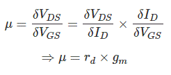
- Small signal amplifiers are made using Field Effect Transistors. They have extremely high input impedance along with a low noise output making them ideal for use in amplifier circuits that have a very small input signal.
- The design of an amplifier circuit is based on the same principle as that for the bipolar transistor circuit used for a Class A amplifier.
- Firstly, a suitable quiescent point or “Q-point” is found for the correct biasing of the JFET amplifier circuit with single amplifier configurations of Common-source (CS), Common-drain (CD) or Source-follower (SF) and the Common-gate (CG).
- These three JFET amplifier configurations corresponds to the common-emitter, emitter-follower and the common-base configurations using bipolar transistors.
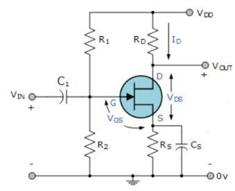
Construction:
- It consists of an N-channel JFET.
- The JFET gate voltage Vg is biased through the potential divider network made by resistors R1 and R2 and its biasing is done within its saturation region.
- JFET takes no input gate current and allows the gate to be treated as an open circuit.
- Hence, no input characteristics curves are required.
- In order to keep the gate-source junction reverse biased, the source voltage, Vs is made higher than the gate voltage, Vg.

- This source voltage is therefore given as:

- Then the Drain current, Id is also equal to the Source current, given as:

- Resistor, Rs and the source by-pass capacitor, Cs serve the same function as the emitter resistor and capacitor in the common emitter bipolar transistor amplifier circuit to provide good stability and prevent a reduction in the loss of the voltage gain.
- The characteristics of a Common Source JFET Amplifier are similar to the common emitter amplifier.
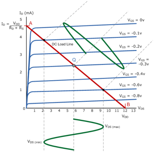
- The actual position of the Q-point is at the mid center point of the load line and is determined by the mean value of Vg.
- The output of the Common Source JFET Amplifier is 180o out of phase with the input signal.
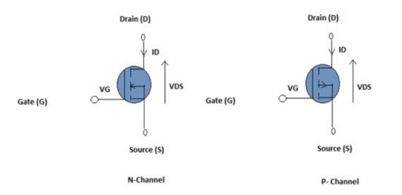
The MOSFET (Metal Oxide Semiconductor Field Effect Transistor) transistor is a semiconductor device which is widely used for switching and amplifying electronic signals in the electronic devices.
It is a core of integrated circuit and is designed and fabricated in a single chip because of its small size.
It is a four terminal device with source(S), gate (G), drain (D) and body (B) terminals.
The body of the MOSFET is connected to the source hence making it a three terminal device like field effect transistor. It can be used in both analog and digital circuits.
The MOSFET works by electronically varying the width of a channel along which charge carriers flow (electrons or holes).
The charge carriers enter the channel through source and exit via the drain.
The width of the channel is controlled by the gate voltage which is located between source and drain.
It is insulated from the channel near an extremely thin layer of metal oxide.
Function:
- Depletion Mode
When there is no voltage on the gate, the channel shows maximum conductance. When the voltage on the gate is either positive or negative, the channel conductivity decreases.
2. Enhancement Mode
The device does not conduct when there is no voltage on the gate. As the voltage increases on the gate, the better the device can conduct.
Working:
The aim of the MOSFET is to be able to control the voltage and current flow between the source and drain. It works like a switch.
The working depends upon the MOS capacitor.
The MOS capacitor is the main part of MOSFET.
The semiconductor surface at the below oxide layer is located between source and drain terminal. It can be inverted from p-type to n-type by applying positive or negative gate voltages respectively.
When the positive gate voltage is applied, the holes present under the oxide layer repel with a repulsive force and holes are pushed downward with the substrate.
The depletion region populated by the negative charges is the acceptor atoms. The positive voltage also attracts electrons. Now, if a voltage is applied between the drain and source, the current flows between the source and drain and the gate voltage controls the electrons in the channel.

References:
1 “Electronic devices and circuit theory” by Boylestead and Nashelsky, Pearson
2 “Electronic principle” by Albert Malvino and Davis J Bates, TMH
3 “Integrated Electronics”, By Jacob Millman and Christos Halkias