UNIT 5
Integrated Circuits
Operational Amplifier
It is commonly known as Op-amp.
It requires an external power source hence is an active device.
It is a versatile device that can be used to amplify ac as well as dc input signals.
It can perform mathematical operations like addition, subtraction, multiplication, integration etc.
Hence was named as Operational Amplifier due to its capability of performing mathematical operations.
When external feedback is provided then the op-amp can be used as ac-dc signal amplifier, oscillator, regulator, active filter etc.
Block Diagram of op-amp

Fig 1: block diagram (Ref: 1)
The block diagram of op-amp consists of :
- Types of inputs
Non-inverting input
Inverting input
- Input stage
It has a dual input.
It is a differential amplifier which provides balanced output.
It provides voltage gain.
Establishes input resistance of op-amp.
- Intermediate stage
It also has a dual input.
It is a differential amplifier which provides unbalanced output.
The output of the input stage becomes input for the intermediate stage.
Due to direct coupling, the dc voltage is well above 0V.
- Level shifting stage
The output of the intermediate stage becomes input for the level shifting stage.
It is an emitter follower with constant current source.
It is used to shift dc level at the output to 0V wrto ground.
- Output stage
This is the final stage.
It’s a push pull amplifier.
It raises swing in output voltage as well as increases current supply capability of op-amp.
Schematic Symbol
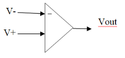
V+ : voltage at inverting input
V- : voltage at non-inverting input
A : voltage gain of op-amp
An ideal op-amp is a differential input, single output device.
It has the following characteristics:
- Infinite input resistance [Ri =∞]
- Zero output resistance [RO = 0]
- Infinite voltage gain [AV = ∞]
- Infinite bandwidth [BW = ∞]
- Infinite Common Mode Rejection Ratio
- Infinite slew rate
- Zero offset [ ie,V1 = V2 , VO =0]
- The above characteristics do not change with the change in temperature.
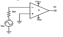
Fig 2: inverting op-amp (Ref: 1)
- As seen in the above figure, input is applied to only one terminal i.e. inverting input terminal.
- The other input terminal is supplied 0V i.e. grounded.
- Hence,
V1 = 0V and V2 = Vin
- Therefore output voltage Vout is given by,
- Vout = A( - Vin )
- Where, A is the voltage gain of op-amp.
- The negative sign implies that the output voltage is 1800 out of phase w.r.to the input voltage.
- Hence, the inverting amplifier amplifies the input signal by voltage gain A and inverts it at the output.
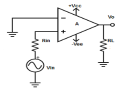
Fig 3: Non inverting amplifier (Ref: 1)
- As seen in the above figure, input is applied to only one terminal i.e. non-inverting input terminal.
- The other input terminal is supplied 0V i.e. grounded.
- Hence,
V1 = Vin and V2 = 0V
- Therefore output voltage Vout is given by,
Vout = AVin
Where, A is the voltage gain of op-amp.
- Here, the output voltage is more than the input voltage by voltage gain A and are also in phase with each other.
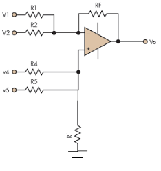
Fig. 4: Summing amplifier (Ref: 1)
- In the above figure, each terminal is connected with two input sources through resistors. V1 and V2 is connected to the inverting terminal and V4 and V5 is connected to the non-inverting terminal.
- Assuming R1=R2=R4=R5=RF=R.
- Now, on applying superposition theorem, for finding output voltage due to V1 alone, keep V2=V4=V5=0V.
- Hence, now the circuit acts as an inverting amplifier.
- Therefore,

- Similarly,

- Now, for V4, voltages V1=V2=V5=0V then the circuit behaves as a non-inverting amplifier.


Hence,


Similarly,

So, the resultant output voltage by all the 4 input voltages is given by,
Vo = V01 + V02 + V04 +V05
Vo = -V1 – V2 +V4 + V5
The output voltage Vo is equivalent to the sum all input voltages applied at both the terminals.
Numerical 1:
In a summing amplifier, if R = 1kΩ, Va = +3V, Vb = +8V, Vc = +9V, Vd = +5V and supply voltage is ±15V. Find the output voltage Vo.
Solution:
Vo = Sum of all input voltages applied at both the terminals
Vo = Va + Vb + Vc +Vd
Vo = -3 -8 +9 +5
Vo = +3V
Numerical 2:
Find the output voltage for the given circuit diagram if Rf = 5kΩ.
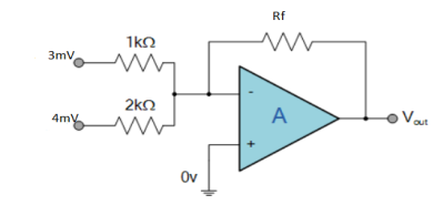
Solution :
We know,
Gain (Av) = =
= 
Hence,
Av1 = 
Av2 = 
Now, Output voltage Vo = Sum of the two amplified input signals
Vo = Av1 x V1 + Av2 x V2
Vo =(-5 x 3) + ( -2.5x 4) mV
Vo = -25mV
As the above output voltage is negative hence it is an inverting amplifier.
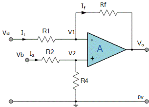
Fig. 5: Difference amplifier
Here input can be provided simultaneously at both the terminals of amplifier.
Voltage signal Va is applied at one input terminal and another voltage signal Vb onto the other input terminal then resultant output voltage is proportional to the “Difference” between the input voltages Va and Vb.
Vo = Vb - Va
Now by applying superposition theorem we get,


Summing point, V1 = V2 and
V2 = Vb 
If Vb = 0 then 
And Va = 0 then 
Vo = -V01 + V02
Vo =  +
+ 
If R1 = R2 and Rf = R4 then

And if R1 = R2 = Rf = R4 =R then
Vo = Vb – Va
Hence, is known as a Unity Gain Differential Amplifier.
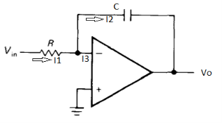
Fig 6 : Integrator
It is a circuit which provides output voltage Vo as an integral form of input voltage Vin.
It is obtained by using an inverting amplifier and replacing its feedback resistor Rf with a capacitor C.
Hence,

Ignoring I3 we have, I3 ≈ 0
So, I1 ≈ I2.
We know current across the capacitor is given by,

Now by applying Kirchoffs current law,

However, V = 0 because gain A is very large

Integrating both sides we get


 + Q
+ Q
Where Q is the integration constant and is proportional to Vo at t = 0 sec .
Therefore, voltage Vo is directly proportional to Vin and inversely proportional to constant RC.
Frequency response of basic integrator circuit is given by,
 ( for 0 db gain)
- A differentiator is a circuit that performs differentiation operation. Hence, the output is a derivative of input.
- In an inverting amplifier, if input resistor is replaced by a capacitor then a differentiator circuit is formed.
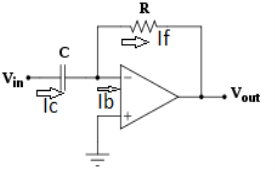
Fig. 7 : Differentiator
- In the above fig. On applying Kirchoff’s law we get,

Since Ib = 0 then,
Ic ≈ If

Since Gain A is very large hence, V1 = 0

Or 
- So, the output voltage is RC times the negative rate of change of input voltage.
- When input is a cosine wave , output is a sine wave i.e. it performs the inverse function of integrator circuit.
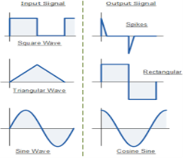
Fig.8: Input and output waveform of differentiator (Ref. 1)
- Frequency response of basic differentiator circuit is given by,
 ( for 0 db gain)
The feedback-amplifier can be defined as an amplifier which has feedback lane that exists between o/p to input. In this type of amplifier, feedback is the limitation which calculates the sum of feedback given in the following amplifier. The feedback factor is the ratio of the feedback signal and the input signal.
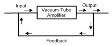
Fig.9 Feedback Amplifier
TYPES
- POSITIVE FEEDBACK AMPLIFIER
The positive feedback can be defined as when the feedback current otherwise voltage is applied for increasing the i/p voltage, then it is named as positive feedback. Direct feedback is another name of this positive feedback. Because positive feedback generates unnecessary distortion; it is not often used in amplifiers. But, it amplifies the original signal power and can be used in oscillator circuits.
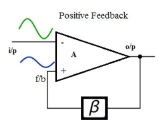
2. NEGATIVE FEEDBACK AMPLIFIER
The negative feedback can be defined as if the feedback current otherwise voltage can be applied for reducing the amplifier i/p, then it is called as negative feedback. Inverse feedback is another name of this negative feedback. This kind of feedback is regularly used in amplifier circuits.

Advantages:
• The amplifier’s gain can be stabilized by the negative feedback
• The particular feedback configurations can be increased by the input resistance.
• Output resistance will be decreased for particular feedback configurations.
• The operating point is stabilized.
Disadvantages:
• The disadvantage of this amplifier is a gain reduction.
Applications:
• Large band width amplifier
• RPS
• Electronic amplifier
References:
1 “Electronic devices and circuit theory” by Boylestead and Nashelsky, Pearson
2 “Electronic principle” by Albert Malvino and Davis J Bates, TMH
3 “Integrated Electronics”, By Jacob Millman and Christos Halkias