Unit 3
Analysis and synthesis of Combinational logic circuits
A comparator is a logic circuit, used to compare the magnitude of two binary numbers.
The following figure shows the block diagram of a n-bit comparator.
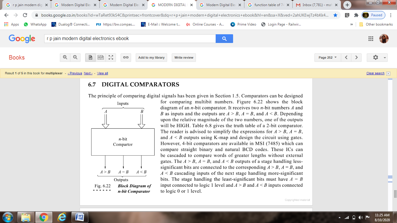
Fig.1: Comparator
It receives two n-bit numbers A and B as inputs and the outputs are A>B,A=B and A<B. Depending upon the relative magnitude of the two numbers, one of the outputs will be high.
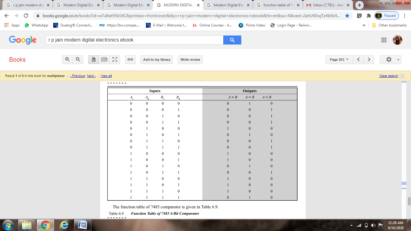
The following is the truth table of a 2-bit comparator.
MULTIPLEXER
Multiplexing means sharing. A multiplexer (MUX) or data selector is a logic circuit that accepts several data inputs and allows only one of them at a time to get through to the output. The routing of the desired data input to the output is controlled by SELECT lines. Block diagram of a MUX with n inputs and one output is shown below:
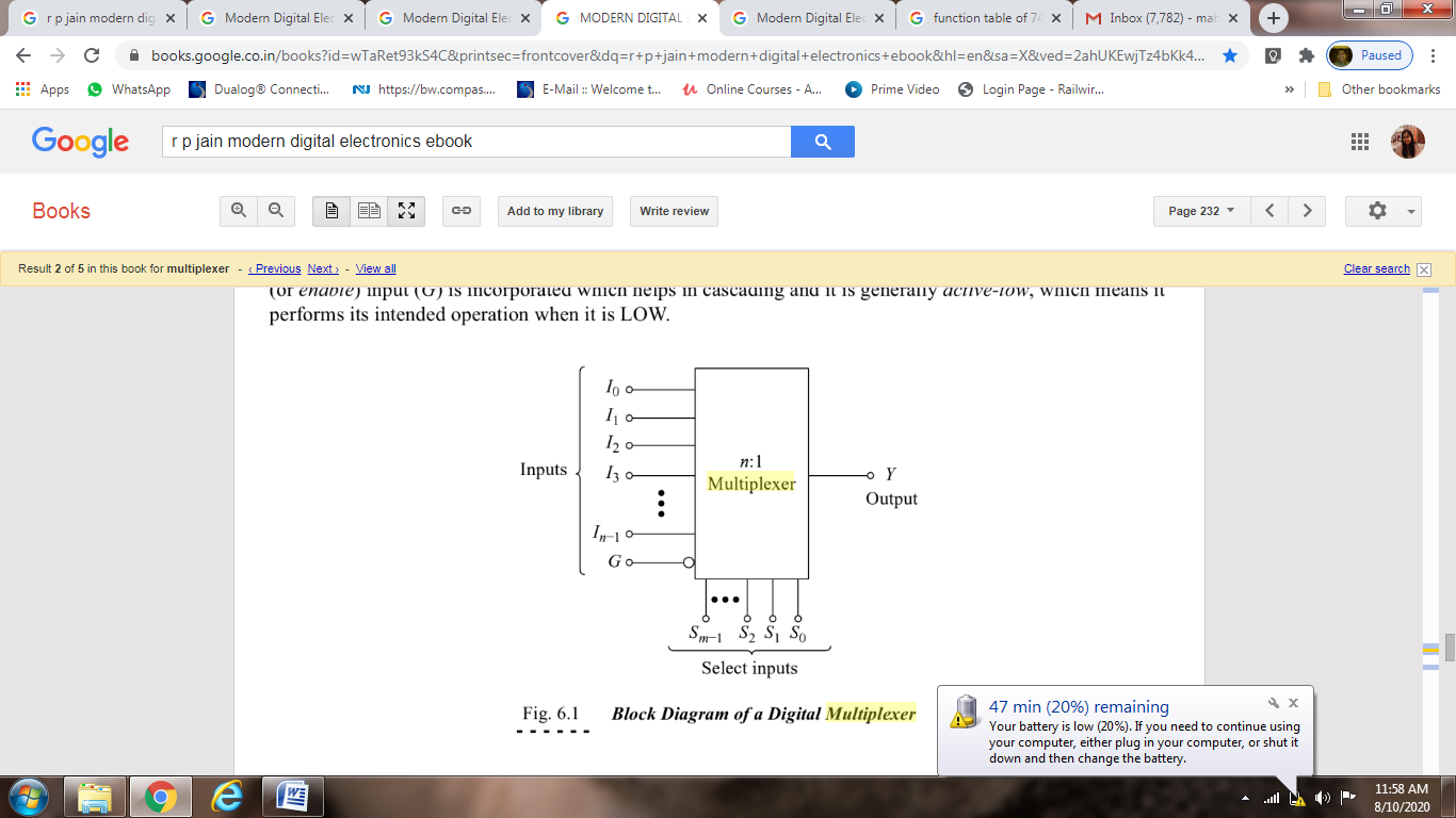
Fig.2: Nx1 MUX
For selecting one out of n inputs for connection to the output, a set of m select inputs is required, where 2m =n. Depending upon the digital code applied at the select inputs, one out of the n-data sources is selected and transmitted to a single output channel.
Normally, an ENABLE input G is incorporated which helps in cascading and is generally active-low. The following is the truth table of a 4:1 MUX with active low enable input G:
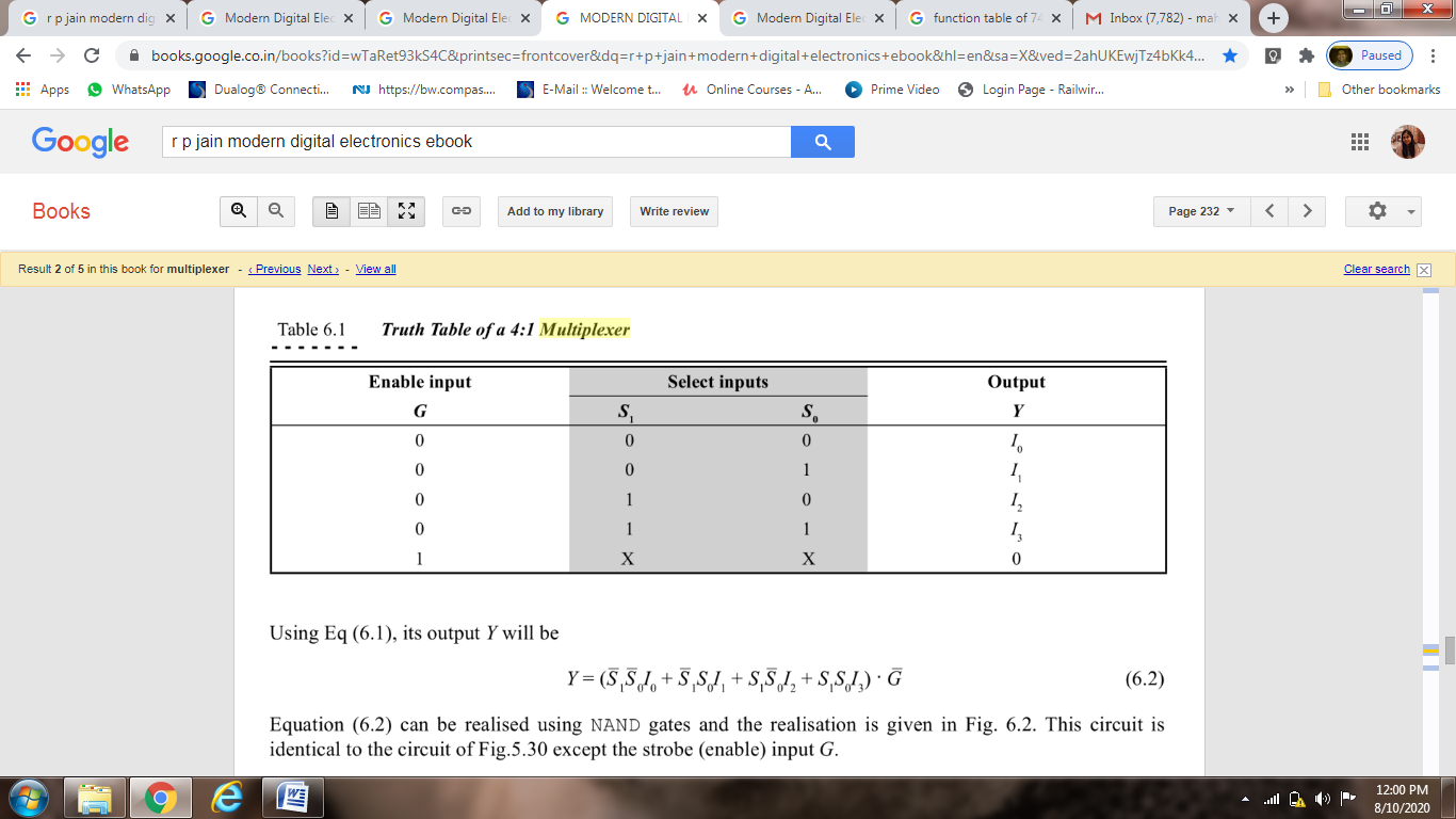
Its output Y can be expressed as: 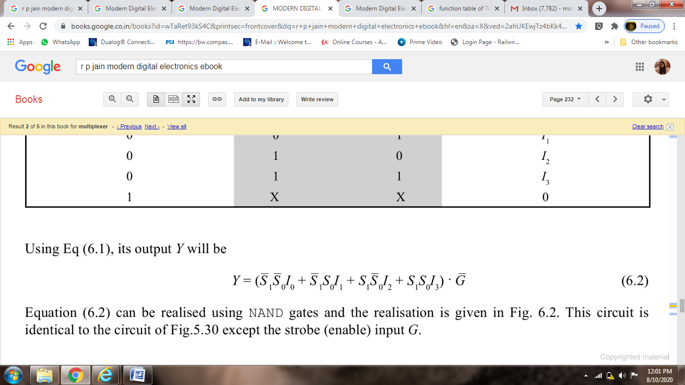
The above equation can be realized using NAND Gates as shown below:
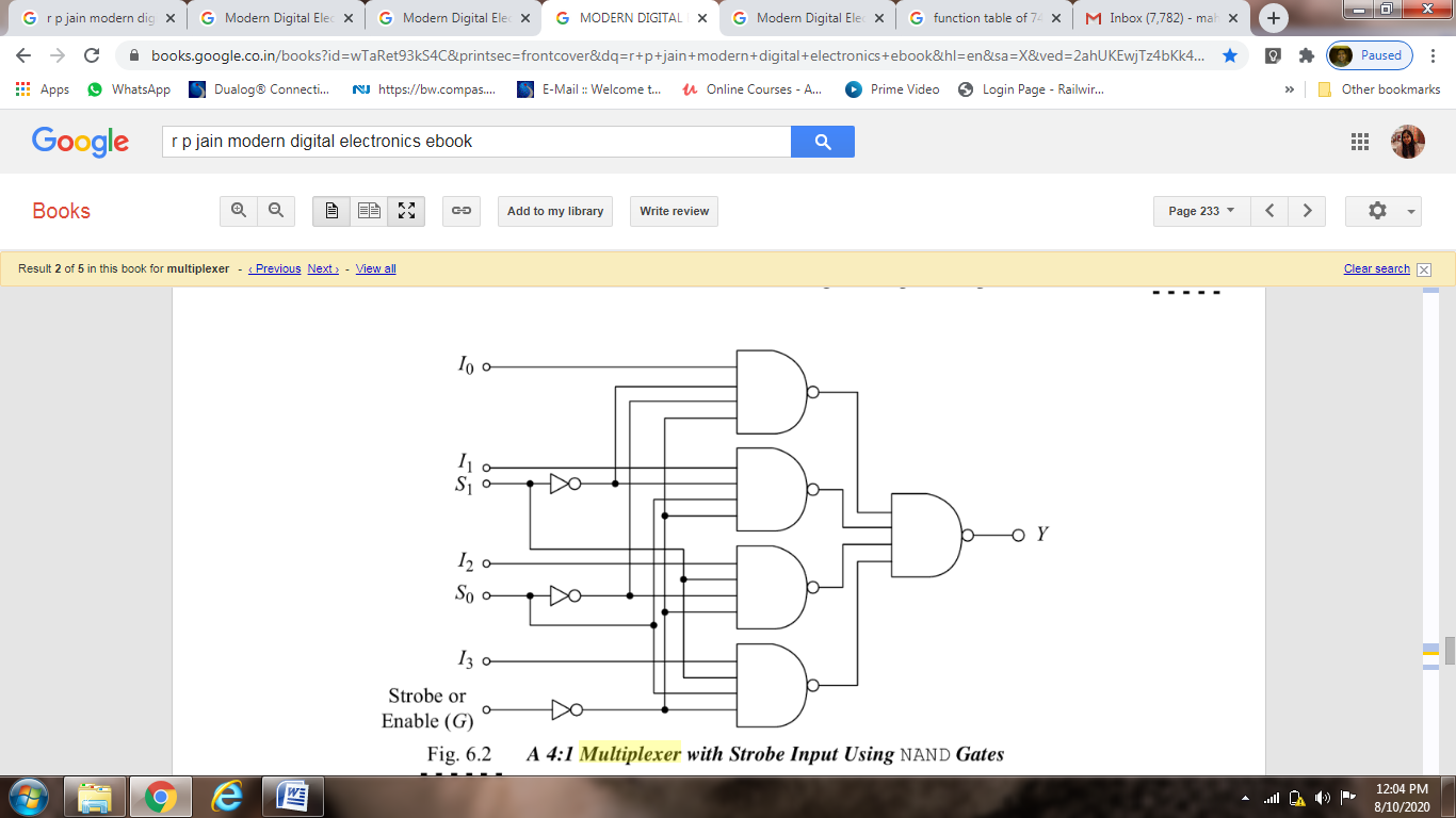
Fig.3: MUX using logic gates
Key Takeaways:
- It has n-data inputs, one output and m inputs select lines with 2m = n.
- The selection of one of the inputs is done by the select lines.
- It is a combinational circuit that converts binary information in the form of a 2N input lines into N output lines, which represent N bit code for the input.
- For simple encoders, only one input line is active at a time.
- For example: Octal to Binary encoder takes 8 input lines and generates 3 output lines.
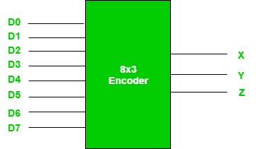
Fig.4 : 8X3 Encoder (ref. 2)
Truth Table –
D7 | D6 | D5 | D4 | D3 | D2 | D1 | D0 | X | Y | Z |
0 | 0 | 0 | 0 | 0 | 0 | 0 | 1 | 0 | 0 | 0 |
0 | 0 | 0 | 0 | 0 | 0 | 1 | 0 | 0 | 0 | 1 |
0 | 0 | 0 | 0 | 0 | 1 | 0 | 0 | 0 | 1 | 0 |
0 | 0 | 0 | 0 | 1 | 0 | 0 | 0 | 0 | 1 | 1 |
0 | 0 | 0 | 1 | 0 | 0 | 0 | 0 | 1 | 0 | 0 |
0 | 0 | 1 | 0 | 0 | 0 | 0 | 0 | 1 | 0 | 1 |
0 | 1 | 0 | 0 | 0 | 0 | 0 | 0 | 1 | 1 | 0 |
1 | 0 | 0 | 0 | 0 | 0 | 0 | 0 | 1 | 1 | 1 |
- From the above truth table it is seen that the output is 000 when D0 is active; 001 when D1 is active; 010 when D2 is active and so on.
Implementation –
- From the above truth table, the output Z is active when the input octal digit is 1, 3, 5 or 7.
- Y is active when input octal digit is 2, 3, 6 or 7 and X is active when input octal digits 4, 5, 6 or 7.
- Hence, the Boolean functions would be:
X = D4 + D5 + D6 + D7
Y = D2 +D3 + D6 + D7
Z = D1 + D3 + D5 + D7
- Hence, the encoder is realised with OR gates as follows:
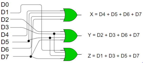
Fig: 5 8:3 encoder (ref.2)
- Limitation of the encoder is that only one input is active at a time.
- If more than one input are active, then the output of encoder is undefined.
- For example, if D6 and D3 are both active, then, our output would be 111 which is the output for D7.
- Problem arises when all inputs are 0.
- The encoder gives output 000 which actually is the output for D0. To avoid this, an extra bit is added to the output which is called the valid bit whose value is 0 when all inputs are 0 or 1.
Key Takeaways:
- It is a combinational circuit that converts binary information in the form of a 2N input lines into N output lines, which represent N bit code for the input.
- For simple encoders, only one input line is active at a time.
- It works as an inverse of an encoder.
- It is a combinational circuit which converts n input lines into 2n output lines.
- Taking an example of 3-to-8 line decoder.
Truth Table –
X | Y | Z | D0 | D1 | D2 | D3 | D4 | D5 | D6 | D7 |
0 | 0 | 0 | 1 | 0 | 0 | 0 | 0 | 0 | 0 | 0 |
0 | 0 | 1 | 0 | 1 | 0 | 0 | 0 | 0 | 0 | 0 |
0 | 1 | 0 | 0 | 0 | 1 | 0 | 0 | 0 | 0 | 0 |
0 | 1 | 1 | 0 | 0 | 0 | 1 | 0 | 0 | 0 | 0 |
1 | 0 | 0 | 0 | 0 | 0 | 0 | 1 | 0 | 0 | 0 |
1 | 0 | 1 | 0 | 0 | 0 | 0 | 0 | 1 | 0 | 0 |
1 | 1 | 0 | 0 | 0 | 0 | 0 | 0 | 0 | 1 | 0 |
1 | 1 | 1 | 0 | 0 | 0 | 0 | 0 | 0 | 0 | 1 |
Implementation
D0 is high when X = 0, Y = 0 and Z = 0. Hence,
D0 = X’ Y’ Z’
Similarly,
D1 = X’ Y’ Z
D2 = X’ Y Z’
D3 = X’ Y Z
D4 = X Y’ Z’
D5 = X Y’ Z
D6 = X Y Z’
D7 = X Y Z
Hence,
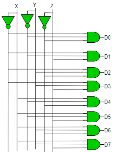
Fig: 6 Decoder (ref.2)
Key Takeaways:
- It works as an inverse of an encoder.
- It is a combinational circuit which converts n input lines into 2n output lines.
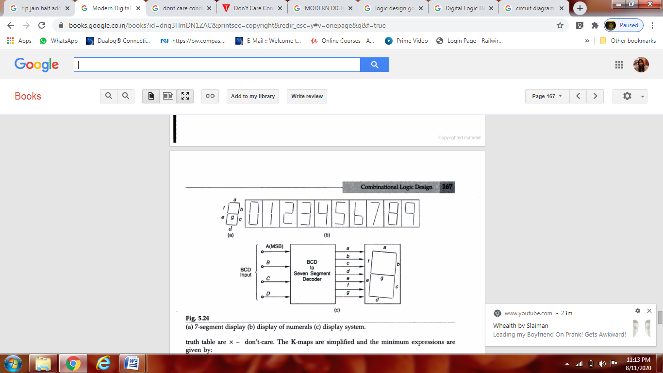
In most practical applications, seven segment displays are used to give a visual indication of the output states of digital IC’s such a decade counters, latches etc. For using this display device, the data has to be converted from some binary code to the code required for the display. Usually, the binary code used is natural BCD.
The following figure shows the display device and the segments which must be illuminated for each of the numerals.
The display system can be connected as follows:
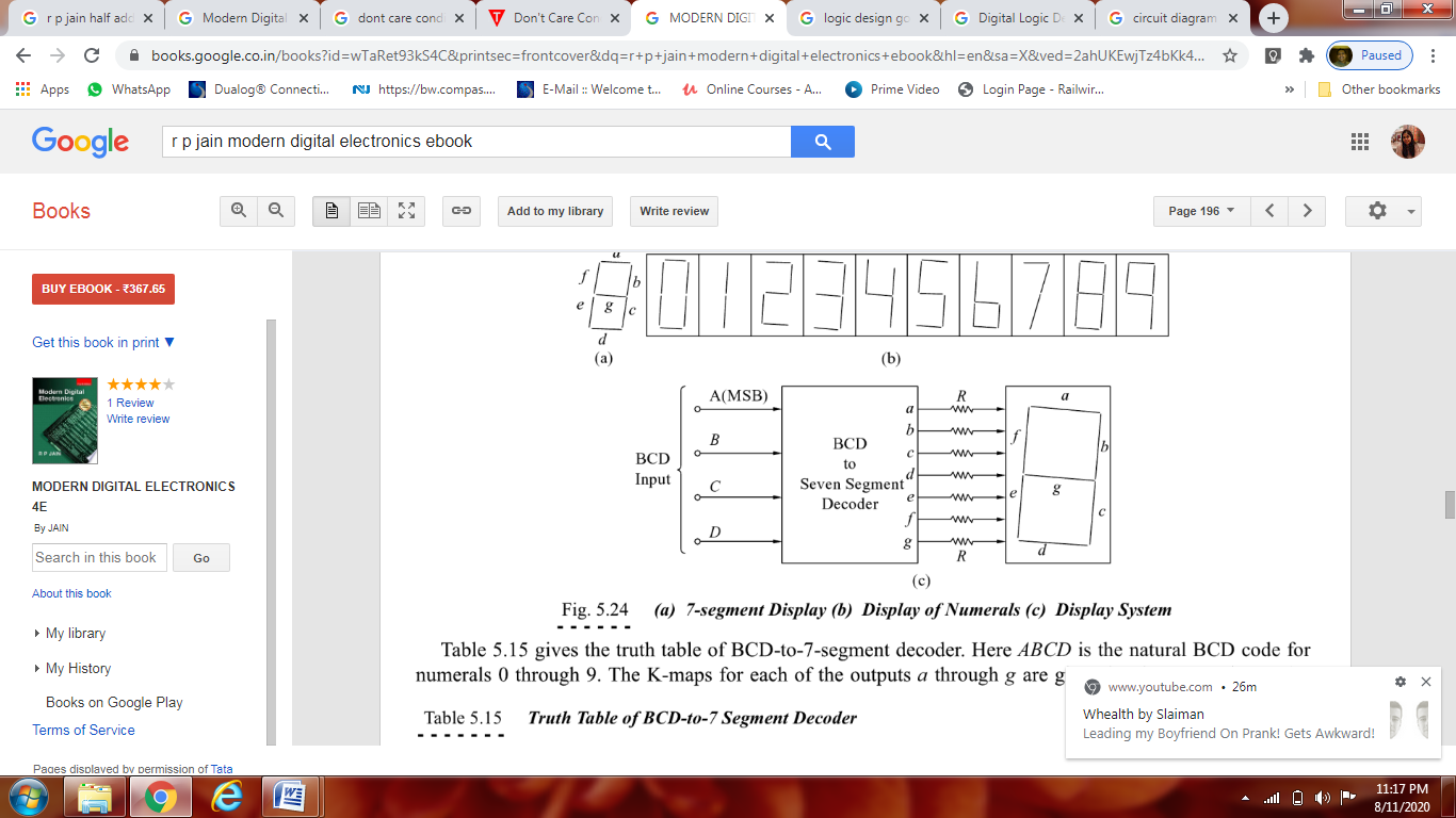
Fig.7: seven segment display
Here, ABCD is the natural BCD code for numerals 0 through 9. Following is the truth table of BCD to 7-segment decoder
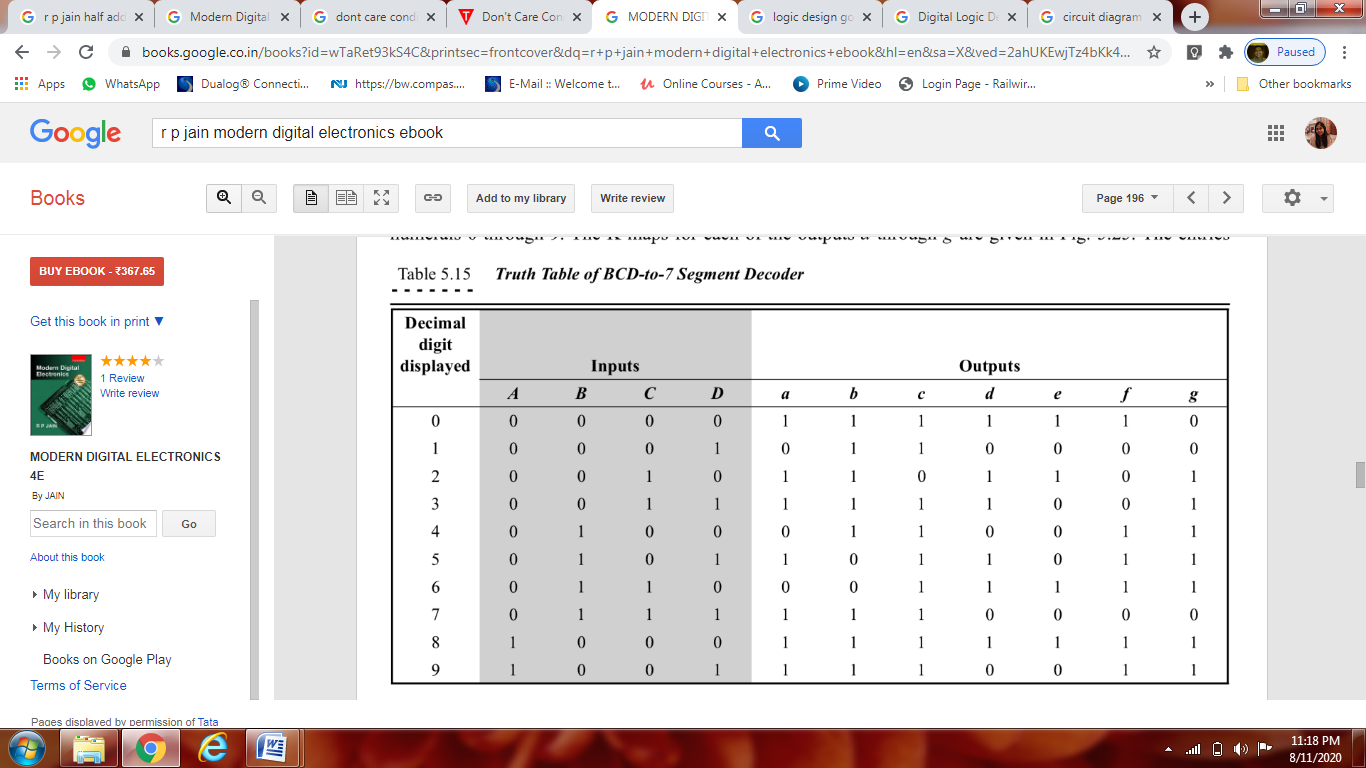
The K-Maps for each of the outputs A through G are given below:
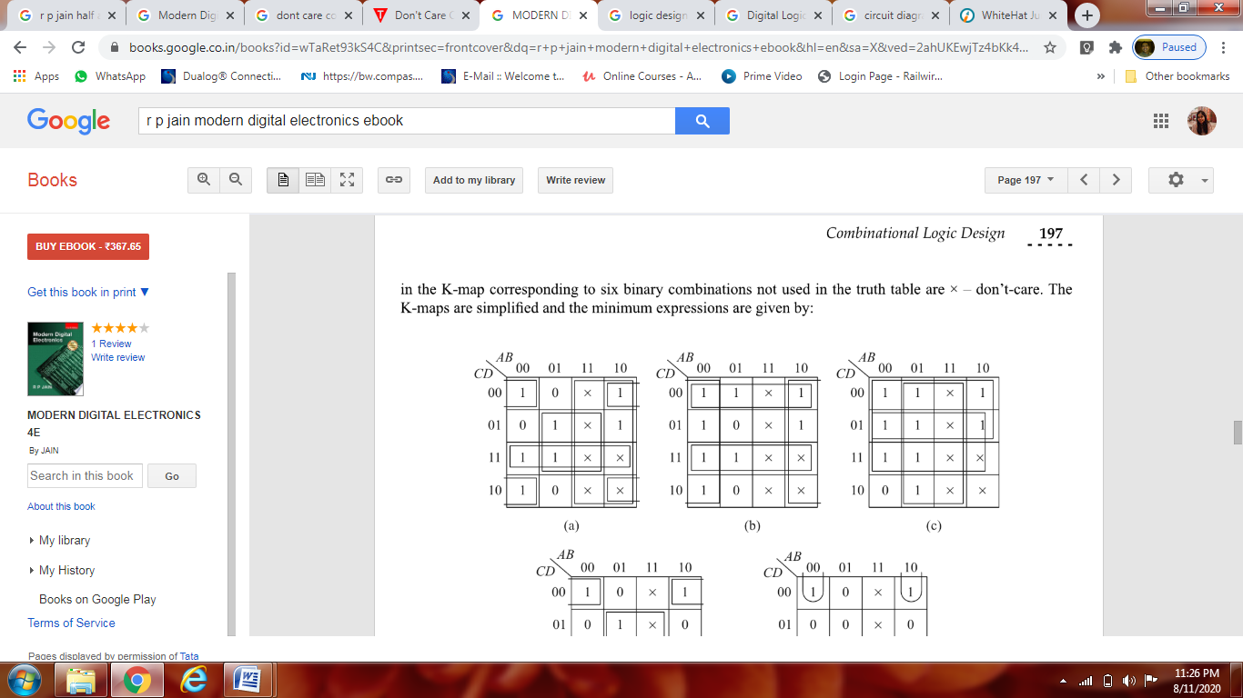
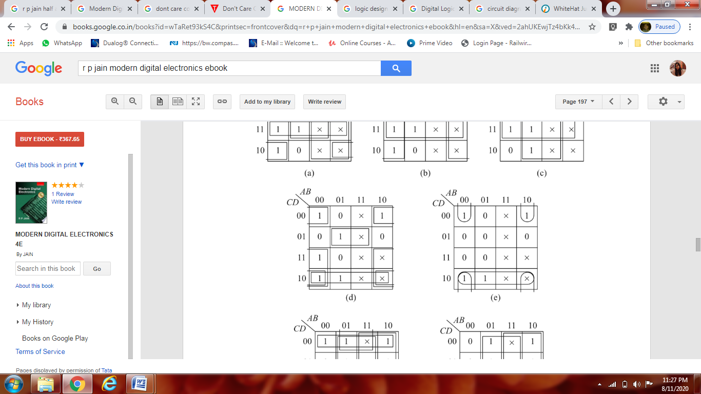
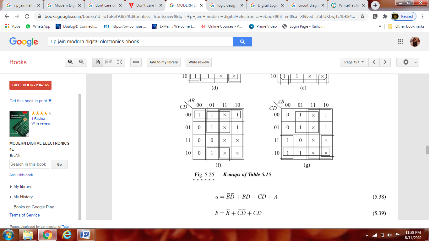
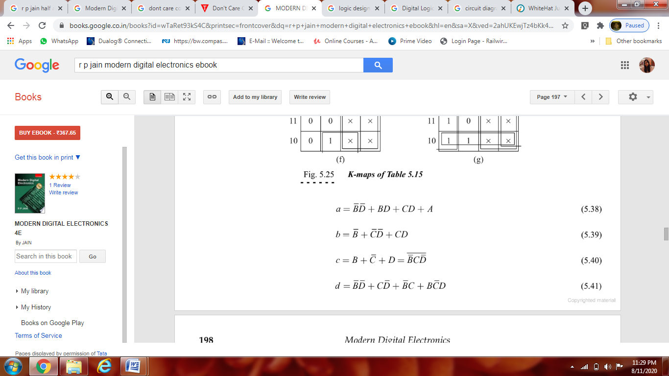
The simplified expressions obtained from the k-maps are:
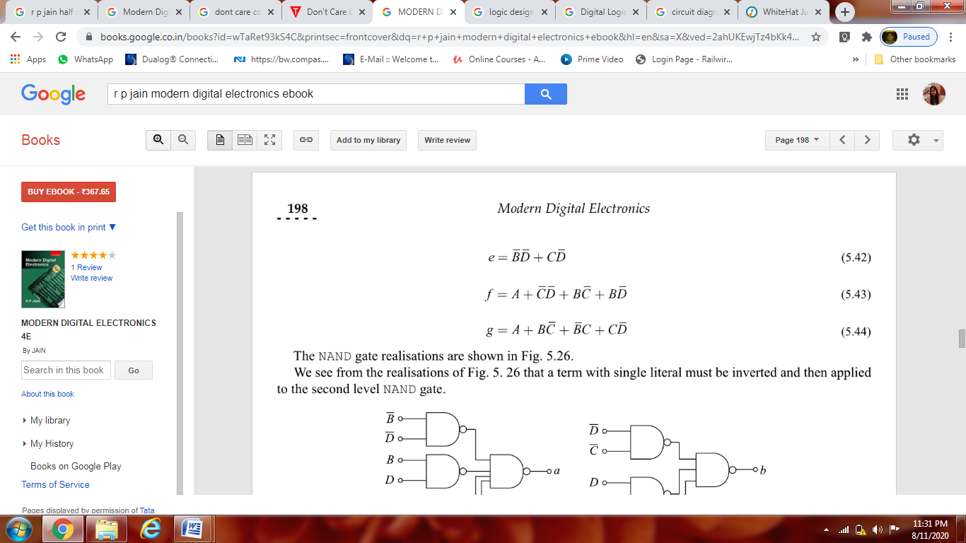
Logic diagram:
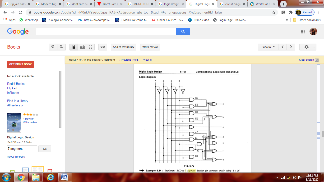
Fig.8: Circuit of 7 segment display
Key Takeaways:
Usually, the binary code used is natural BCD.
- Half Adder
It is a combinational circuit which has two inputs and two outputs.
It is designed to add two single bit binary number A and B.
It has two outputs carry and sum.
Block diagram
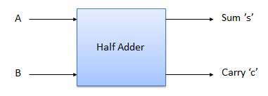
Fig. 9: Half adder (ref. 2)
Truth Table
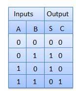
Circuit Diagram
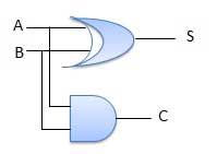
Fig.10: Half adder (ref. 2)
B. Full Adder
It is developed to overcome the drawback of Half Adder circuit.
It can add two one-bit numbers A and B and a carry C.
It is a three input and two output combinational circuit.
Block diagram
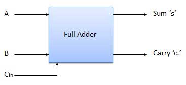
Fig.11: Full adder (ref. 2)
Truth Table
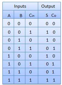
Circuit Diagram
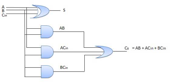
Fig.12: Full adder (ref. 2)
Key Takeaways:
- Half adder is a combinational circuit which has two inputs and two outputs.
- Since there is no provision for carry in half adder, full adder is developed to overcome the drawback.
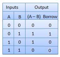
Half Subtractors
It is a combination circuit with two inputs and two outputs.
The difference between the two binary bits is obtained at the output and an output (Borrow) indicates if a 1 has been borrowed.
Here A is called Minuend bit and B is called a Subtrahend bit.
Truth Table
Circuit Diagram
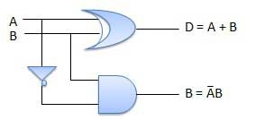
Fig.13: Half subtractor (ref. 2)
Full Subtractors
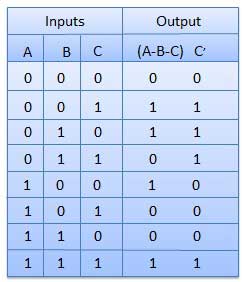
It is a combinational circuit which has three inputs A, B, C, and two output D and C'.
A is the 'minuend', B is 'subtrahend', C is the 'borrow' which is produced by the previous stage, difference output D and C' is the borrow output.
Truth Table
Circuit Diagram
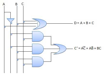
Fig.14: Full subtractor (ref. 2)
Key Takeaways:
- Half subtractor is a combinational circuit which has two inputs and two outputs.
- Since there is no provision for borrow in half subtractor, full subtractor is developed to overcome the drawback.
- Serial Adder:
A serial adder is used to add two binary numbers in serial form. The two binary numbers to be added serially are stored in two shift registers. The circuit adds one pair at a time with the help of one full adder. The carry output from the full adder is applied to a D flip-flop, the output of which is then used as a carry input for the next pair of significant bits. However the sum bit S from the output of the full adder can be transferred into a third shift register.
2. Parallel Adder:
A parallel adder is a combinational digital circuit that adds two binary numbers in parallel form. It consists of full adders connected in cascade, with the output carry from each full adder connected to the input carry of the next full adder.
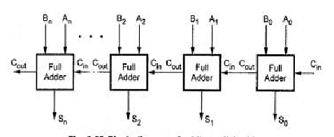
Fig.15: Parallel Adder
BCD stands for binary coded decimal.
Suppose, we have two 4-bit numbers A and B. The value of A and B can vary from 0(0000 in binary) to 9(1001 in binary).
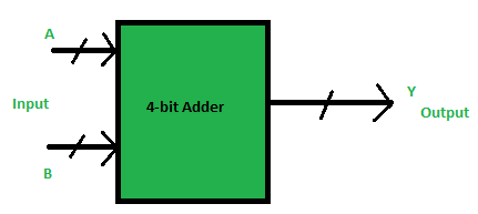
Fig.16 : BCD adder (ref. 2)
The output varies from 0 to 18 if the carry from the previous sum is not considered.
But if we consider the carry, then the maximum value of output will be 19 (i.e. 9+9+1 = 19).
When we simply add A and B, then we get the binary sum, and to get the output in BCD form, we use BCD Adder.
Key Takeaways:
- BCD stands for binary coded decimal.
Example 1:
Input :
A = 0111 B = 1000
Output :
Y = 1 0101
Explanation: We are adding A(=7) and B(=8).
The value of the binary sum will be 1111(=15).
But, the BCD sum will be 1 0101,
Where 1 is 0001 in binary and 5 is 0101 in binary.
Example 2:
Input :
A = 0101 B = 1001
Output :
Y = 1 0100
Explanation: We are adding A(=5) and B(=9).
The value of the binary sum will be 1110(=14).
But, the BCD sum will be 1 0100,
Where 1 is 0001 in binary and 4 is 0100 in binary.
Now, let's move to the table and find out the logic when we are going to add “0110”.
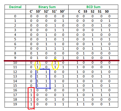
Fig.17 : Table explaining BCD addition (ref. 2)
We are adding “0110” (=6) only to the second half of the table because of the following conditions:
- If C’ = 1 (Satisfies 16-19)
- If S3′.S2′ = 1 (Satisfies 12-15)
- If S3′.S1′ = 1 (Satisfies 10 and 11)
So, our logic is
C' + S3'.S2' + S3'.S1' = 1
Implementation :
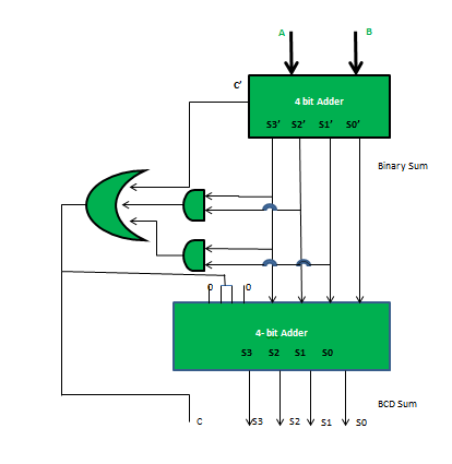
Fig.18 : BCD adder (ref. 2)
Reference Books:-
1) “Digital Fundamentals”, Floyd and Jain, Pearson
2) “Digital Logic and Computer design”, M. Morris Mano, Pearson
3) “Fundamentals of Digitals Circuits”, A. Anand Kumar, PHI
4) “Digital Systems”, Ronald J. Tocci, Neal S. Widmer, Pearson