Unit 7
Use of building blocks
- It is commonly referred as DAC, D/A or D2A.
- It is a device that converts binary values (0s and 1s) into a set of continuous analog voltages.
- A computer operating in an analog world, is a binary machine, that produces an output which is understood by other devices.
DAC Working
The binary system is a positional and a place value system, where each bit represents the presence or absence of a certain power of two in the total sum of the powers.
In other words, the whole DAC process is like a scaling operation where the binary count is mapped to a certain voltage range, keeping 0V minimum and the maximum voltage is input binary voltage.
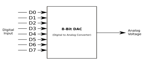
Fig.1: DAC
Key Takeaways:
- It is commonly referred as DAC, D/A or D2A.
- It is a device that converts binary values (0s and 1s) into a set of continuous analog voltages.
In the weighted resistor type DAC, each digital level is converted into an equivalent analog voltage or current.
The following figure is the binary weighted resistor type DAC.
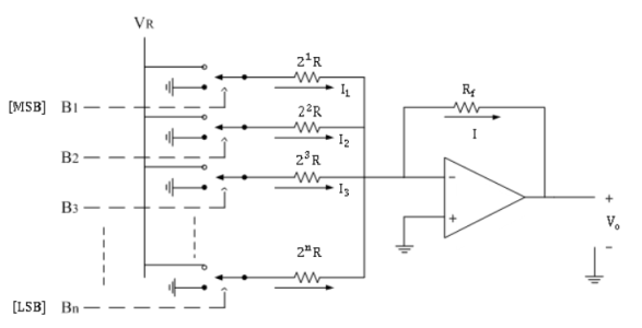
Fig.2: Weighted resistor
Here 
It consists of parallel binary weighted resistor bank and a feedback resistor Rf.
The switch positions decide the binary word (i.e.B1B2B3…Bn).
Here, op-amp is used as current to voltage converter.
Disadvantages:
1) When number of binary input increases, it is not easy to maintain the resistance ratio.
2) Very wide ranges of different values of resistors are required.
R-2R
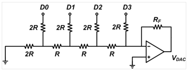
Fig.3:R-2R
Circuit Operation
Assume that D0 is connected to VREF and the other bits are logic low
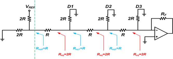
Applying the Thevenin theorem

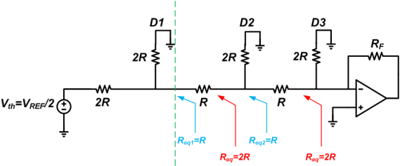
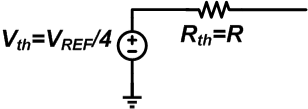
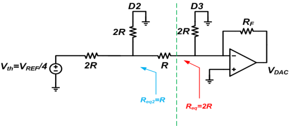
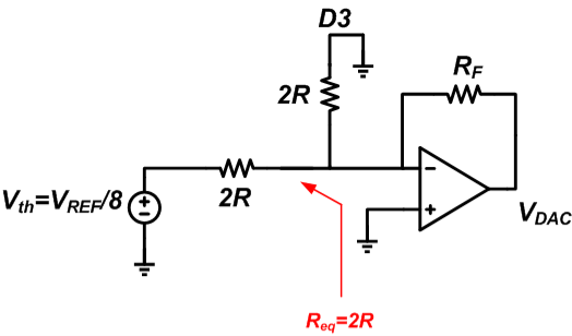
Assuming RF=2R, the output voltage will be VDAC = -2R ✖ (VREF/8)/2R = -VREF/8.
This output voltage corresponds to the DAC LSB.
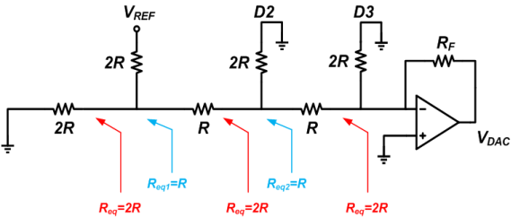
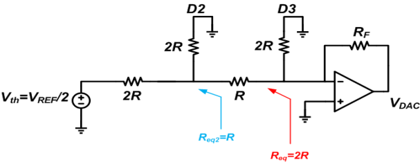
This is the same as Figure 9 except that the input is VREF/2 instead of VREF/4. Considering the result of the case D3D2D1D0 = 0001, if RF = 2R we obtain VDAC = -VREF/4.
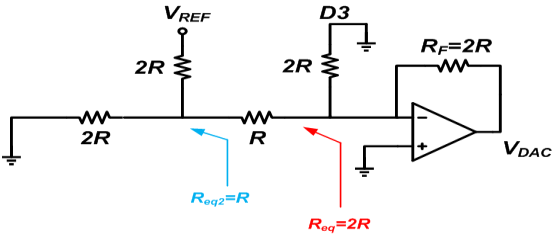
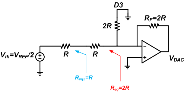
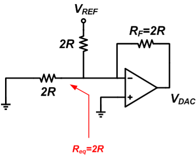
The output voltage will be VDAC = -(VREF/2R)✕2R = -VREF.
- Analog to Digital Converters (ADC) is used to translate analog electrical signals for data processing purposes.
- With products matching performance, power, cost, and size needs, analog devices offers large A/D converter.
- These data converters ensure accurate and reliable conversion performance in fields such as communications, energy, healthcare, etc.
Counter ADC
The counter type ADC is made using a binary counter, DAC and a comparator. The output voltage of a DAC is equivalent to corresponding digital input to DAC.
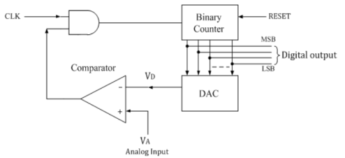
Fig.4: Counter ADC
Operation:
The n-bit binary counter is initially set to 0 by using reset command.
Therefore the digital output is zero and the equivalent voltage is also 0V.
When the reset command is removed, the clock pulses go through AND gate and are counted with the binary counter.
DAC converts the digital output to an analog voltage and applies as an inverting input to the comparator.
The output enables the AND gate to pass the clock.
The number of clock pulses increases with the increase in time and the analog input voltage is a rising staircase waveform.
The counting continues until the DAC output equals and just rises more than unknown analog input voltage.
Then the comparator output becomes low and this disables the AND gate from passing the clock.
The counting stops when VA< VD.
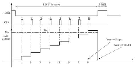
Fig.5: Counter ADC output
Succession ADC
Successive Approximation type ADC is the most widely used and popular ADC method.
The conversion time is maintained constant in successive approximation type ADC, and is proportional to the number of bits in the digital output, unlike the counter1and continuous type A/D converters.
The basic principle is that the unknown analog input voltage is approximated against an n-bit digital value by trying one bit at a time, starting with the MSB.
It operates by successively dividing the voltage range by half.
(1) The MSB is initially set to 1 with the remaining three bits set as 000. The digital equivalent voltage is compared with the unknown analog input voltage.
(2) If the analog input voltage is higher than the digital equivalent voltage, the MSB is retained as 1 and the second MSB is set to 1
Example:
Let us assume that the 4-bit ADC is used and the analog input voltage is VA = 10V. When the conversion starts, the MSB bit is set to 1.
Now VA = 10V > VD = 8V = [1000]2
Since the unknown analog input voltage VA is higher than the equivalent digital voltage VD, as discussed in step (2), the MSB is retained as 1 and the next MSB bit is set to 1 as follows
VD = 12V = [1100]2
Now VA = 11V < VD = 12V = [1100]2
Here now, the unknown analog input voltage VA is lower than the equivalent digital voltage VD. As discussed in step (2), the second MSB is set to 0 and next MSB set to 1 as
VD = 10V = [1010]2
Now again VA = 9V > VD = 9V = [1001]2
Again as discussed in step (2) VA>VD, hence the third MSB is retained to 1 and the last bit is set to 1. The new code word is
VD = 10V = [1010]2
Now finally VA = VD , and the conversion stops.
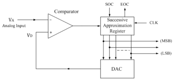
Fig.6: Succession ADC
It consists of a successive approximation register (SAR), DAC and comparator. The output of SAR is given to n-bit DAC. The equivalent analog output voltage of DAC, VD is applied to the non-inverting input of the comparator. The second input to the comparator is the unknown analog input voltage VA. The output of the comparator is used to activate the successive approximation logic of SAR.
When the start command is applied, the SAR sets the MSB to logic 1 and other bits are made logic 0, so that the trial code becomes 1000.
Key Takeaways:
Advantages:
- Conversion time is less.
- Conversion time is constant and independent of the amplitude of the analog input signal.
Disadvantages:
- Circuit is complex.
- The conversion time is more.
Reference Books:-
1) “Digital Fundamentals”, Floyd and Jain, Pearson
2) “Digital Logic and Computer design”, M. Morris Mano, Pearson
3) “Fundamentals of Digitals Circuits”, A. Anand Kumar, PHI
4) “Digital Systems”, Ronald J. Tocci, Neal S. Widmer, Pearson