UNIT 2
Band theory of Solids
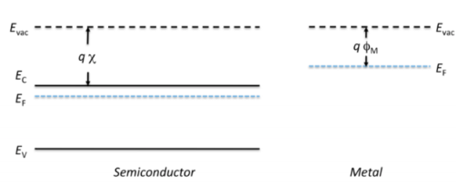
Energy has to be supplied to shift electrons away from the nucleus of the atom. The valence electrons have the top energy level of the electrons that still hurdle to their parent atoms, (as they are farthest away from the nucleus). Supplementary energy is necessary to fully eliminate an electron from the atom, so free electrons have top energy levels than valence electrons. (Free Electrons are called the movable charge carriers that allow metals to conduct electrical energy.) This can be explained with the help of an energy band diagram, which has two energy levels, a valence band, and a conduction band.

Fig.2.1 Energy Band Diagram
In semiconductors, there is a space connecting the valence and conduction bands. Energy should be supplied for valence electrons to "shoot up" to the conduction band. This reflects the piece of information that energy must be supplied to eliminate valence electrons from their parent atoms and develop into free electrons. In insulators this space is larger, to signify the higher energy levels that would be required, to "drag" electrons from their parent atoms. In metals, the valence band, and conduction band overlap. So in metals, valence electrons can move effortlessly into the conduction band, producing a huge number density of free electrons.
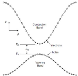
The material characteristics of a particular Semiconductor are shown by an E-K diagram. It shows the bond among the energy and momentum of existing quantum mechanical states for electrons in the material.
First, consider a basic E-k band diagram like this one (the x-axis can be momentum, pp, or wavenumber, kk, since p=ℏkp=ℏk):

Fig.2.2 E-K Diagram
In the above figure you can notice a small number of things:
- The bandgap (EG), which is the variation in energy among the top of the valence band and the base of the conduction band.
- The effective mass of electrons and holes in the material. This is given by the curvature of each of the bands.
- This diagram indicates how the actual electron states are uniformly spaced in k-space. This means that the density of states in E (ρ (E) ρ (E)) depends on the slope of the E-k curve.
Normally when we see the E-K diagram it corresponds to the reduced zone. The highest filled energy level is the valence band and the next one is the conduction band when we look into these bands and draw the reduced picture we focus on K vs. E part of the diagram. In semiconductors, we consider the top of the valence band and bottom of the conduction band. When we calculate the density of states, the density of state in a band is extremely large and the charge carrier responsible for the flow of current is extremely small therefore only the electrons close to the bottom of the conduction band and holes near to the top of valence band participate in the whole process of conduction.
Insulators are materials that reduce the flow of electrical current. The contrary of conductors, which permit electric current to pass without restraint, insulators are implemented in domestic objects and electrical circuits as a defense. Thermal insulation is alike, but it constricts the flow of heat rather than electricity.

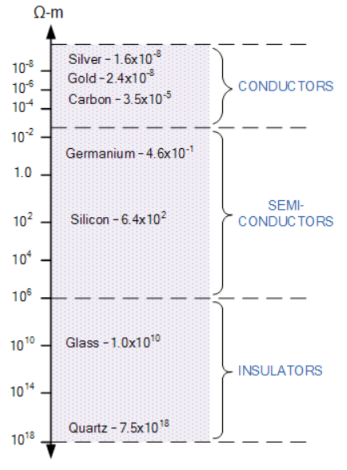
Fig.2.3 Condutors and Semi conductors
Conductors are materials that have very low values of resistivity, usually in the micro-ohms per metre. This low value allows them to easily pass an electrical current due to there being plenty of free electrons floating about within their basic atom structure. But these electrons will only flow through a conductor if there is something to spur their movement, and that something is an electrical voltage.
Semiconductors are materials which have a conductivity between conductors (generally metals) and nonconductors or insulators (such as most ceramics). Semiconductors can be pure elements, such as silicon or germanium, or compounds such as gallium arsenide or cadmium selenide. In a process called doping, small amounts of impurities are added to pure semiconductors causing large changes in the conductivity of the material.
References:
i) Electrical Engineering Materials, Dr. G.P. CHHALOTRA & Dr. B.K.BHAT, Khanna Technical Publications.