UNIT-5
INTRODUCTION TO UJT
Unijunction Transistor or UJT
Construction
The UJT is a three-terminal device having one emitter junction and two base ohmic contacts. The device has evolved from the alloyed germanium bar structure and the structure was called a filamentary transistor.
The symbol for UJT is shown in Figure 1.
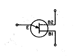 |
Figure 1: Symbol for UJT
The two ohmic contacts are called base 1 (B1) and base 2 (B2). The p-n junction located between B1 and B2 is called the emitter junction. The equivalent circuit of a UJT is shown in Figure 1.
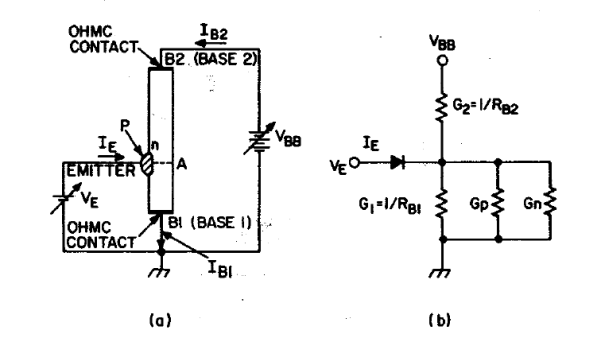 |
Figure 2: (a) UJT Structure (b) Equivalent structure of UJT
As the device developed through the cube UJT, the diffused planar structure, and the epitaxial planar structure, the terms "double-base diode" and finally "unijunction transistor" were coined for the device.' A schematic diagram of a UJT is shown in Figure2(a).
In the normal operating condition, the base 1 terminal is grounded and a positive bias voltage VBB is applied at base 2 Figure2(a). The resistance between B1 and B2 is designated by RBB, that between B2 and A by RB2, and that between A and B1 by RB1 (RBB =RB2 + RB1). The Gpand Gn are the excess hole and electron conductance between the emitter and base 1.
Working
The applied voltageVBB establishes a current and an electric field along the semiconductor bar and produces a voltage on the n side of the emitter junction, which is a fraction ηof the applied voltage VBB. The fraction η is called the intrinsic stand-off ratio and is given by

When the emitter voltage VE is less than ηVBB, the emitter junction is reverse-biased and only a small reverse saturation current flows in the emitter circuit. If the voltage VE exceeds ηVBB by an amount equal to the forward voltage drop of the emitter junction, holes will be injected into the bar. Because of the electric field within the semiconductor bar, these holes will move toward base 1 and increase the conductivity of the bar in the region between the emitter and base 1. As IE is increased, the emitter voltage will decrease because of the increased conductivity, and the device will exhibit a negative resistance characteristic.
Characteristics
The characteristics of Unijunction Transistor (UJT) can be explained by three parameters Cutoff, Negative Resistance Region and Saturation.The device characteristic are shown in Figure 3.
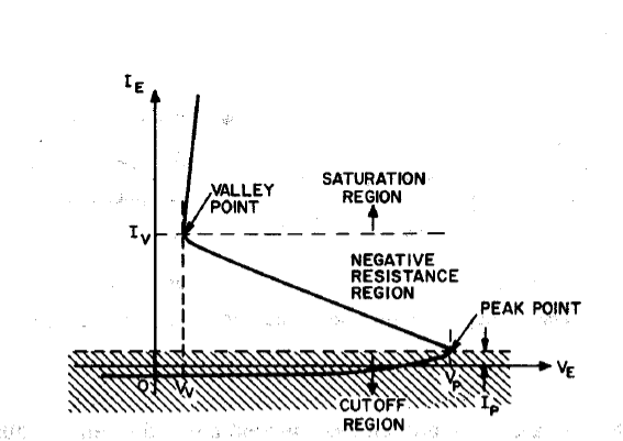 |
Figure3: The device characteristic
- Cut off: The two important points on the curve are the peak point and the valley point. At these two points the slope dVE/dIE= 0. The region with current less than Ip is called the cut-off region (OFF state). Cutoff region is the area where the Unijunction Transistor (UJT) doesn’t get sufficient voltage to turn on. The applied voltage hasn’t reached the triggering voltage, thus making transistor to be in off state.
- Negative Resistance Region: The region between the peak and valley part is called the negative resistance region; here the conductivity modulation is important. When the transistor reaches the triggering voltage, Unijunction Transistor (UJT) will turn on. After a certain time, if the applied voltage increases to the emitter lead, it will reach out at peak voltage. The voltage drops from peak voltage to Valley Point even though the current increases (negative resistance).
- Saturation: The region with current larger than Iv is called the saturation region (ON state). The switching time from the peak to the valley point depends on the device geometry and the biasing condition. The time is proportional to the distance between the emitter and base 1 contact.
Application
- Switching Device
- Triggering Device for Triacs and SCR’s
- Timing Circuits
- For phase control
- In saw tooth generators
- In simple relaxation oscillators
Key Takeaways
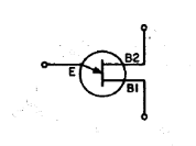
- The UJT is a three-terminal device having one emitter junction and two base ohmic contacts. The symbol for UJT is shown in Figure
 |
- The applied voltage VBB establishes a current and an electric field along the semiconductor bar and produces a voltage on the n side of the emitter junction, which is a fraction ηof the applied voltage VBB.
- The fraction η is called the intrinsic stand-off ratio and is given by

- The characteristics of Unijunction Transistor (UJT) can be explained by three parameters Cut-off, Negative Resistance Region and Saturation.
The silicon controlled rectifier (SCR) is a three-terminal semiconductor switching. It is considered important circuit element after the diode and the transistor. This name is given to this device because it is made of silicon and is used as a rectifier and that rectification can be controlled.
Silicon controlled rectifier is a semiconductor device that acts as a true electronic switch. It can change alternating current into direct current and simultaneously can control the amount of powered to the load. Thus SCR combines the features of a rectifier and a transistor.
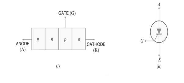 |
Figure 4: (i) construction (ii) the symbol of SCR.
Construction
The three pn junction device is called a silicon-controlled rectifier. It is formed as when a pn junction is added to a junction transistor, It is an ordinary rectifier (pn) and a junction transistor (npn) combined in one unit to form pn pn device.
There are three terminals
- One from the outer p-type material called anode.
- A second from the outer n-type material called cathode K.
- The third from the base of transistor section and is called gate G.
In the normal operating conditions of SCR, anode is held at high positive potential w.r.t. Cathode and gate at small positive potential w.r.t. Cathode.
The silicon-controlled rectifier is a solid state equivalent of thyratron. The gate, anode and cathode of SCR correspond to the grid, plate and cathode of thyratron. For this reason, SCR is sometimes called thyristor.
Working
In a silicon-controlled rectifier, load is connected in series with anode. The anode is always kept at positive potential w.r.t. Cathode.
The device is made of silicon because leakage current in silicon is very small as compared to germanium.
The device is used as a switch, it will carry leakage current in the off condition which should be as small as possible.
- When gate is open: In case of open gate no voltage applied to the gate. When gate is open, junction J2 is reverse biased while junctions J1 and J3 are forward biased. Hence, the situation in the junctions J1 and J3 is just as in a npn transistor with base open. Consequently, no current flows through the load RL and the SCR is cut off. However, if the applied voltage is gradually increased, a stage is reached when reverse biased junction J2 breaks down. The SCR is in the ON state i.e. conducts heavily. The applied voltage at which SCR conducts heavily without gate voltage is called Break over voltage. Figure 5 shows the SCR circuit with gate open.
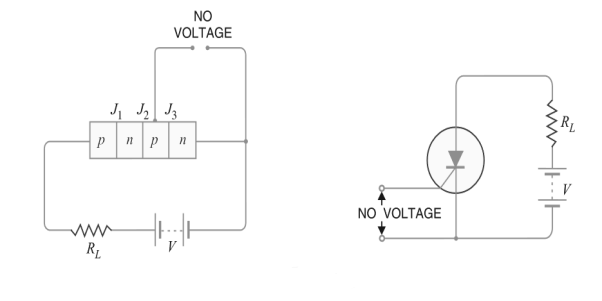 |
Figure 5: When gate is open
- When gate is positive w.r.t. Cathode: In this case junctionJ3 is forward biased and junction J2 is reverse biased. Now the electrons from n-type material start moving across junction J3 towards left whereas holes from p-type towards the right. Consequently, the electrons from junction J3 are attracted across junction J2 and gate current starts flowing.
As soon as the gate current flows, anode current increases. The increased anode current in turn makes more electrons available at junction J2. This process continues and in an extremely small time, junction J2breaks down and the SCR starts conducting heavily.
Once SCR starts conducting, the gate loses all control. Even if gate voltage is removed, the anode current does not decrease at all. The only way to stop conduction i.e. bring SCR in off condition by reducing the applied voltage to zero.
So the SCR can be made to conduct heavily at smaller applied voltage by applying a small positive potential to the gate as shown in Figure 6.
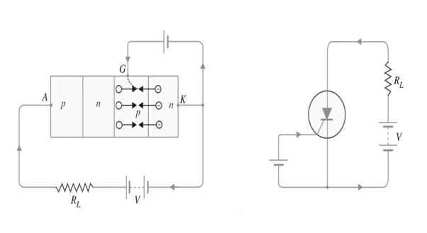 |
Figure 6: When gate is positive w.r.t. Cathode
The following conclusions are drawn from the working of SCR
(i)SCR behaves like a switch. An SCR work between two states i.e. either it does not conduct or it conducts heavily. There is no state in between.
(ii)There are two ways to turn on the SCR. The first method is to keep the gate open and make the supply voltage equal to the breakover voltage. The second method is to operate SCR with supply voltage less than breakover voltage and then turn it on by means of a small voltage applied to the gate.
(iii)Applying small positive voltage to the gate is the normal way to close an SCR because the breakover voltage is usually much greater than supply voltage.
(iv)To open the SCR (i.e. to make it non-conducting), reduce the supply voltage to zero.
Equivalent Circuit of SCR
The SCR shown in Figure 7(ii) can be visualised as separated into two transistors as shown in
 |
Figure 7: (i) construction of SCR (ii) Thus, the equivalent circuit of SCR is composed of pnp transistor and npn transistor connected as shown in (iii) It is clear that collector of each transistor is coupled to the base of the other, thereby making a positive feedback loop.
Characteristics
It is the curve between anode-cathode voltage (V) and anode current (I)of an SCR at constant gate current. Figure 8 shows the characteristics of SCR.
(i) Forward characteristics: When anode is positive w.r.t. Cathode, the curve between V and I is called the forward characteristic. In Figure 8 OABC is the forward characteristic of SCR at IG=0. If the supply voltage is increased from zero, a point is reached (point A) when the SCR starts conducting. Under this condition, the voltage across SCR suddenly drops as shown by dotted curve AB and most of supply voltage appears across the load resistance RL. If proper gate current is made to flow, SCR can close at much smaller supply voltage.
(ii) Reverse characteristics: When anode is negative w.r.t. Cathode, the curve between V and I is known as reverse characteristic. The reverse voltage does come across SCR when it is operated with a.c. Supply. If the reverse voltage is gradually increased, at first the anode current remains small (i.e. leakage current) and at some reverse voltage, avalanche breakdown occurs and the SCR starts conducting heavily in the reverse direction as shown by the curve DE. This maximum reverse voltage atwhich SCR starts conducting heavily is known as reverse breakdown voltage.
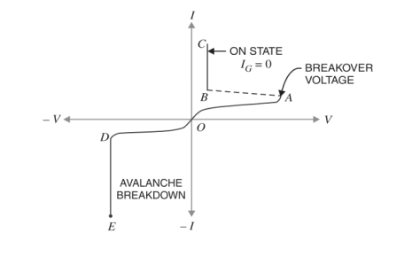 |
Figure 8: Characteristics of SCR
Applications of SCR
The ability of an SCR to control large currents in a load by means of small gate current makes this device useful in switching and control applications. Some of the important applications of SCR are:
- An important application of SCR is for switching operations. As SCR has no moving parts, therefore, when it is used as a switch, it is often called a static contactor.
- SCR used for power control. It is often necessary to control power delivered to some load such as the heating element of a furnace. Series resistances or potentiometers cannot be used because they waste power in high power circuits. Under such conditions, silicon controlled rectifiers are used which are capable of adjusting the transmitted power with little waste.
- SCRs used for speed control of d.c. Shunt motor. The conventional method of speed control of d.c. Shunt motor is to change the field excitation. But change in field excitation changes the motor torque also. This drawback is overcome in SCR control.
- SCR used for overlight detection.
- SCR Crowbar. A crowbar is a circuit that is used to protect a voltage-sensitive load from excessive d.c. Power supply output voltages.
Key Takeaways
- The three pn junction device is called a silicon controlled rectifier.
- Silicon controlled rectifier is a semiconductor device that acts as a true electronic switch.
- There are three terminals one from the outer p-type material called anode, a second from the outer n-type material called cathode K, the third from the base of transistor section and is called gate G.
- In the normal operating conditions of SCR, anode is held at high positive potential w.r.t. Cathode and gate at small positive potential w.r.t. Cathode.
- In case of open gate, no voltage applied to the gate. When gate is open, junction J2 is reverse biased while junctions J1 and J3 are forward biased.
- When gate is positive w.r.t. Cathode junction J3 is forward biased and junction J2 is reverse biased.
- SCR behaves like a switch. An SCR work between two states i.e. either it does not conduct or it conducts heavily. There is no state in between.
- Applying small positive voltage to the gate is the normal way to close an SCR because the break over voltage is usually much greater than supply voltage.
- To open the SCR (i.e. to make it non-conducting), reduce the supply voltage to zero.
- When anode is positive w.r.t. Cathode, the curve between V and I is called the forward characteristic.
- When anode is negative w.r.t. Cathode, the curve between V and I is known as reverse characteristic.
TRIAC
Triac can conduct in both the directions that is whether the applied gate signal is positive or negative. Triac is a three terminal AC switch and itis different from the other silicon-controlled rectifiers. This is a three terminal, four layer, bi-directional semiconductor device that controls AC power. Schematic Symbol of Triac is shown in figure
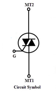 |
Figure 9: Schematic Symbol of Triac
Construction
It consists of three terminals namely, main terminal 1(MT1orM1), main terminal 2(MT2orM2), and gate terminal G. Triac is bilateral since it works for both the polarities. Triac do not have anode and cathode.
In the structure of triac, two SCRs are connected in the anti-parallel and it will act like a switch for both the directions. Gate terminals is connected to both the N and P regions due to which gate signal may be applied which is irrespective of the polarity of the signal
Here the gate terminal is the control terminal. The flow of current in the triac is bi directional that means current can flow in both the directions.
The triac structure is considerably more complicated than a conventional thyristor. In addition to the p1-n 1-p2-n2 basic four layers, there are a junction gate n3 region and a n4 region in contact with M1. Note also that p1 is shorted to n4, p2 is shorted to n2, and n3 is shorted to p2 by M1, M2, and the gate electrode, respectively.
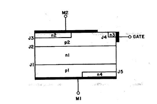 |
Figure 10: Basic Structure of Triac
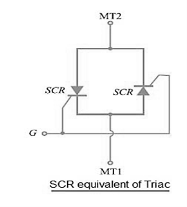 |
Figure 11: SCR equivalent of Triac
Working
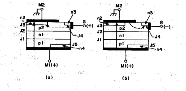
Triac can switch the current in either direction by applying low voltage or by low current pulse of either polarity between the gate and one of the two main terminals M1 and M2. The device operations under various biasing conditions are illustrated as:
- When the main terminal M1 is positive with respect to M2 and a positive voltage is applied to the gate (also with respect to M2): in this case the device behaviour is identical to that of a conventional thyristor. The junction J4 is reverse-biased and is inactive; the gate current is supplied through the gate short near the n3 region. Since junction J5 is also reverse-biased and inactive, the main current is carried through the left side of p1-n 1-p2-n2 section. Shown in Figure 12(a)
- M1 is positive with respect to M2, but a negative voltage is applied to the gate: The junction J4 between n3 and p2 is now forward-biased, and electrons are injected from the n3 to p2. The auxiliary thyristor pl-nl-p2-n3will be turned on by the flow of the lateral base current in p2 toward the n3 gate because of the gain increase in the transistor n3-p2-nl. Full conduction of this auxiliary thyristor results in the current flowing out of this device and toward the n2 region. This current will provide the required gate current and trigger the left-side p1-n1-p2-n2 thyristor into conduction. . Shown in Figure 12(b)
|
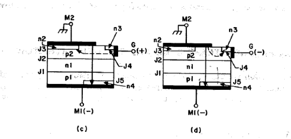
Figure 12: Current flow in four different triggering modes in Triac
Iii. When Ml is negatively biased with respect to M2 and VG is positively biased: In this case the junction J3 becomes forward-biased between M2 and the shorted gate. Electrons are injected from n2 to p2 and diffuse to nl, resulting in an increase of the forward bias of J2. By the regenerative action, eventually full current is carried through the short at M2. The gate junction J4 is reverse-biased and is inactive. The full device current is carried through the right-side p2-nl-pl-n4 thyristor. Shown in Figure 12(c)
Iv. Ml negative with respect to M2 and VG is also negative: In this condition, the junction J4 is forward-biased, and triggering is initiated by injection of electrons from n3 to n1 region. This action lowers the potential at n1, causing holes to be injected from p2 into it n1 region. These holes provide the base current drive for the p2-n1-p1 transistor, and the right side p2-n1-p1-n4 thyristor is eventually turned on since J3 is reverse-biased, the main current is carried from the short at M2 through the n4 region. Shown in Figure 12(d)
Characteristics
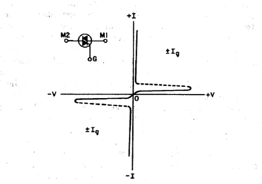 |
Figure 13: Current–Voltage Characteristics of a triac
The gate trigger may occur in any four quadrant modes of operation. If the device is in ON state the conduction permits a huge amount of current to flow through it.
The current–voltage characteristics of a triac are shown in Figure 13. The supply voltage of the triac to switch ON depends upon the gate current. The triac is a symmetrical triode switch that can control loads supplied with ac power. The V-I characteristics of triac in the first and third quadrants are basically equal to those of an SCR in the first quadrant. It can be functioned with either +Ve or –Ve gate control voltage but in typical operation generally the gate voltage is +Ve in first quadrant and -Ve in third quadrant.
A large amount of current is controlled by the resistance, otherwise, the device may be damaged. With the device, the gate is a control terminal and the proper signal is applied to the gate, therefore the firing angle of the device is controlled.
Applications
TRIAC (Triode for AC) is the semiconductor device widely used in power control and switching applications. The triac is very useful in light dimming, motor speed control, temperature control, and other applications. It finds applications in switching, phase control, chopper designs, brilliance control in lamps, speed control in fans, motors etc.
DIAC
DIAC simply means diode alternating current or diode ac switch. The DIAC is nothing but the combination of two SCRs connected back to back. So A DIAC is a two-terminal device that can act as a switch based on the voltage applied across it.
We already studied that the TRIAC being used to switch current in both directions. But TRIACs cannot fire/trigger symmetrically it is accompanied by a support component called DIAC. Generally, DIAC uses to trigger the TRIAC. Sometimes it is also known as a TRIAC without GATE terminal.
SYMBOL OF DIAC
The symbol of DIAC is as shown in figure.
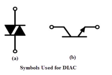 |
Figure 14: Symbol of DIAC
DIAC is given by the symbol of two Diodes connected in parallel and opposite to one another and has two terminals. Since the DIAC is bidirectional.
These two terminals can’t be named as anode and cathode, these terminals are labelled MT1 and MT2 where MT stands for Main terminals or simply M1 and M2. In some books terminals are labelled as A1 and A2. Just like a resistor or ceramic capacitor the pinouts of DIAC are reversible.
Construction
We already know that the DIAC is a two-terminal device. Diac is simply a combination of parallel semiconductor layers that allows activating in one direction. It can deliver current flow in both directions. DIAC consists of two terminals namely MT1 and MT2. The Structure is similar to that of transistor, but difference is the DIAC does not have any base terminal. A DIAC has two p-type material and three n-type materials and it does not have any gate terminal in it.
The three region have the same amount of doping and it delivers symmetrical switching properties in both the polarities of the applied voltage. The layers closer to the terminals are the combination of both positive and negative layers. When the voltage is passed to the terminals the layer with respective polarity to the voltage gets activated, this combination of both the polarities helps in operating the DIAC in both the directions
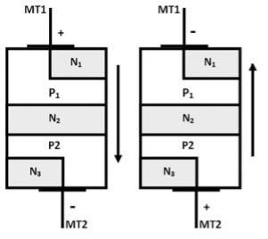 |
Figure 15: Construction of DIAC
Working
When a voltage of either polarity is applied to a diac, one junction is forward-biased and the other is reverse-biased. The current is limited by the leakage current of the reverse-biased junction. When the applied voltage is sufficiently large, breakdown occurs at BVCBO(1 -  , where BVCBOis the avalanche breakdown voltage of the p-n junction, the common-base current gain, and it is a constant. This expression is the same for the breakdown voltage of an open base n-p-n transistor.
As the current increases after breakdown,  will increase, causing a reduction of the terminal voltage. This reduction gives rise to the negative region. The bidirectional p-n-p-n diode switch behaves like two conventional Shockley diodes connected in antiparallel to permit the accommodation to voltage signals of two polarities, as in figure 16(a), where M1 stands for main terminal 1, and M2 for main terminal 2. Using the shorted-cathode principle, we can integrate this arrangement into a single two-terminal diac as shown in Figure 16(b). The symmetry of this structure results in identical performance for either polarity of applied voltage. The diac can be triggered into conduction by exceeding the breakover voltage or by dV/dt triggering. Because of its regenerative action, the indirection p-n-p-n diode switch has a larger negative resistance and smaller forward drop than that of an ac trigger diode.
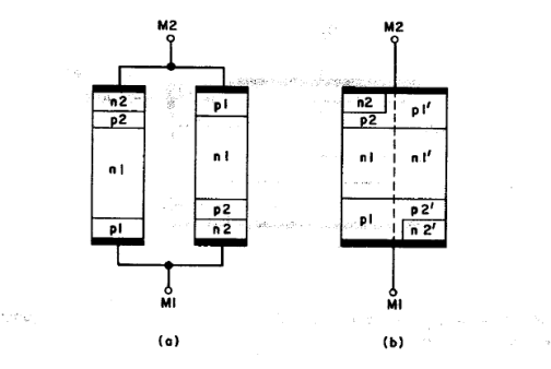 |
Figure 16: (a) Two shockley devices are connected antiparallel (b) Integration of the diodes into two terminal single device Construction of DIAC
Characteristics
Curve of the DIAC will be in the shape of a Z and the curve will be lying on the first and third quadrants because they conduct in both the positive and negative polarity. The First quadrant represents the positive half cycle where the current will be flowing from MT1 to MT2 (or M1 to M2) and the second quadrant represents the negative half cycle where the current will be flowing from MT2 to MT1(or M2 to M1). The symmetrical I-V characteristics are shown in Figure 17.
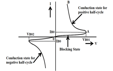 |
Figure 17: I-V characteristics of DIAC
Initially, because of the Reverse Biasing between the layers there will be small leakage current flowing through the DIAC i.e. the resistance of the DIAC will be higher. It is called as the blocking state in the curve.
Once the applied voltage reaches the breakdown voltage the resistance of the DIAC drops abruptly and then it starts conducting which leads to a sharp decrease in voltage and the current starts increasing, which is mentioned as a conduction state in the curve.
The DIAC will be in the conducting state until the current reaches the particular value called the holding current, where holding current is the minimum current that required for a device to keep it in the ON state.
The DIAC acts as an open circuit when the voltage is less than its avalanche breakdown voltage. When the device has to be turned off, the voltage must be reduced below its avalanche breakdown voltage.
Application of DIAC
The main application of a DIAC is its use in a TRIAC triggering circuit. The DIAC is connected to the gate terminal of the TRIAC. When the voltage across the gate decreases below a predetermined value, the gate voltage will be zero and hence the TRIAC will be turned off. When the applied voltage across the DIAC increases above the avalanche breakdown voltage, only then it can conduct.
DIAC can be used in the lamp dimmer circuit, in a heat control circuit and in the speed control of a universal motor
Key Takeaways
- Triac can conduct in both the directions that is whether the applied gate signal is positive or negative.
- Triac is a three terminal AC switch and it is different from the other silicon controlled rectifiers.
- Triac is bilateral since it works for both the polarities. Triac do not have anode and cathode.
- The gate terminal is the control terminal. The flow of current in the triac is bi directional that means current can flow in both the directions.
- The TRIAC device operations under various biasing conditions are illustrated as:
- When the main terminal M1 is positive with respect to M2 and a positive voltage is applied to the gate (also with respect to M2
- M1 is positive with respect to M2, but a negative voltage is applied to the gate:
- When Ml is negatively biased with respect to M2 and VG is positively biased:
- Ml negative with respect to M2 and VG is also negative
- DIAC simply means diode alternating current or diode ac switch.
- The DIAC is nothing but the combination of two SCRs connected back to back. So A DIAC is a two-terminal device that can act as a switch based on the voltage applied across it.
- Generally, DIAC uses to trigger the TRIAC. Sometimes it is also known as a TRIAC without GATE terminal.
- Initially, because of the Reverse Biasing between the layers there will be small leakage current flowing through the DIAC i.e. the resistance of the DIAC will be higher. It is called as the blocking state in the curve.
- Once the applied voltage reaches the breakdown voltage the resistance of the DIAC drops abruptly and then it starts conducting which leads to a sharp decrease in voltage and the current starts increasing, which is mentioned as a conduction state in the curve.
- The main application of a DIAC is its use in a TRIAC triggering circuit.
The UJT is often use data trigger device for SCR’s and TRIAC’s.Other application sincludenon-sinus oidaloscillators; saw tooth generators, phase control, and timing circuits. The most common UJT circuit in use today is the relaxation oscillator.
The pulse signal required for digital circuits can be obtained from a single stage oscillator circuits using a particular device like unijunction transistor. Such an oscillator which uses UJT is called UJT relaxation oscillator.
The basic circuit of UJT relaxation oscillator is shown in the Figure 18.
The R1 and R2 are known as biasing resistances. R1 and R2 are current limiting resistors. The value of these resistances is chosen such that they are lower than inter-base resistances RB1 and RB2.
The oscillating rate is decided by the value of resistance RT and the capacitance CT. Resistor RT and capacitor CT determines the frequency of the oscillator. The value of RT is so selected that the operating point of UJT remains in the negative resistance region.
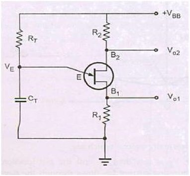 |
Figure 18: UJT relaxation oscillator
Working
Capacitor CT gets charged through the resistance RT towards supply voltage VBB as long as the capacitor voltage is less than peak voltage Vp the emitter appears as an open circuit.
As the Emitter of the UJT is connected to the capacitor, when the charging voltage VcT across the capacitor becomes greater than the diode volt drop value, i.e. the capacitor voltage Vc exceeds the voltage Vp, the p-n junction behaves as a normal diode and becomes forward biased triggering the UJT into conduction.
The capacitor starts discharging through R1 +RB1 where RB1 internal base resistance. As RB1 is assumed negligible and hence capacitor discharges through R1. Due to the design of R1 this discharge is very fast, and it produces a pulse across R1
As the ohmic value of resistorCT is very low, the capacitor discharges rapidly through the UJT and a fast rising voltage pulse appears across R1. Also, because the capacitor discharges more quickly through the UJT than it does charging up through resistor RT, the discharging time is a lot less than the charging time as the capacitor discharges through the low resistance UJT.
When the capacitor voltage falls below Vv i.e. VC = VE= VV the UJT gets turned OFF. The capacitor starts charging again. The discharge time of the pulse is controlled by the time constant CTR1 while the charging time constant by RTCT.
The UJT characteristics and the negative resistance region of the characteristics are shown in the Figure 19. The characteristics of UJT show the variation between V and I where VE is emitter voltage and IE is emitter current.
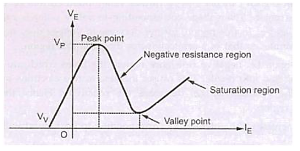 |
Figure 19: characteristics of UJT
When the capacitor is discharged to the valley point voltage “Vv” the emitter to RB1 resistance climbs again and the capacitor starts charging. This cycle is repeated and results in a sort of sawtooth waveform across the capacitor. The saw tooth waveform across the capacitor of a typical UJT relaxation oscillator is shown in the figure below.
From the output voltage wave form it is clear that the output pulses has a very small width and that along relaxation time ex its between the two pulses.Therefore it is said that the device is relaxed in this duration and is called the relaxation oscillator.
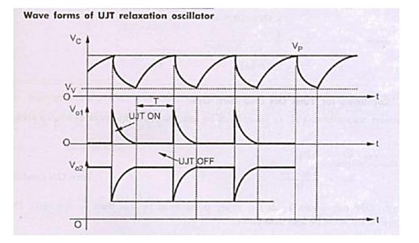 |
Figure 20: Waveforms of UJT relaxation oscillator
There is voltage drop across R2 and voltage rise across R1, when UJT fires. The charging equation of the capacitor is given by,
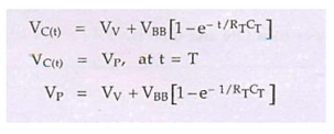 |
The period of oscillation is given by

Key Takeaways
- The pulse signal required for digital circuits can be obtained from a single stage oscillator circuits using a particular device like unijunction transistor. Such an oscillator which uses UJT is called UJT relaxation oscillator.
- The value of these resistances is chosen R1 and R2 such that they are lower than inter-base resistances RB1 and RB2.
- The oscillating rate is decided by the value of resistance RT and the capacitance CT.
- The value of RT is so selected that the operating point of UJT remains in the negative resistance region.
- From the output voltage waveform it is clear that the output pulses has a very small width and that along relaxation time exits between the two pulses.
- The charging equation of the capacitor is given by,
 |
- The period of oscillation is given by

P-I-N AND AVALANCHE
p-i-n Diode
In p-i-n diode an “intrinsic” (actually lightly doped) I region is sandwiched between heavily doped p- and n-regions. It is p-i-n diode is a three-region structure
In the p-i-n photodiode shown schematically in Figure 21.An opening is made in the surface metallization to admit light, the top semiconductor region is kept very thin no minimize absorption in the region and the i-layer width is specifically tailored so achieve the desired response characteristics. Because of the low doping the i-layer is totally depleted under zero bias or becomes depleted at small reverse biases.
Furthermore, the heavy doping of the outer p and n regions causes the depletion widths in these regions Tobe very narrow. Thus as pictured in a Figure 22
The depletion width inside the device is effectively equal to the i-layer width independent of the applied reverse bias. The energy bands (in Figure 22) are linear functions of position and the ξ-field is approximately constant in the i-region because of the low semiconductor doping.
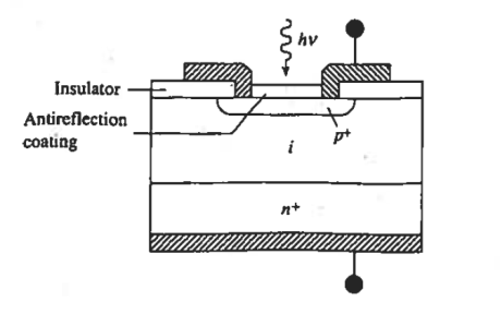 |
Figure 21: p-i-n photodiode Cross section.
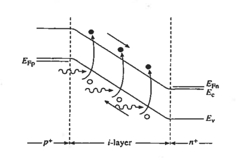 |
Figure 22: p-i-n photodiode Reverse bias energy band diagram.
It should also be noted than the heavy doping of the outer p and n regions causes the depletion means the minority carriers diffusion lengths in these regions will be relatively small. Asa result, the greater part of the photocurrent flowing in a p-i-n photodiode arises from carriers generated in the central depletion region.
Operational advantages of the p-i-n photodiode that have made it one of the most widely employed photodetectors stem, from the existences and tailor ability of the i-region.
For one, the diode con be optimized for response at a given wavelength by making the layer width equal to the inverse of the absorption coefficient (1/ ) of the specified wavelength Second, with one of the most photocurrent arising from light absorption to the i-region. Frequency response is greatly enhanced over that of a pn junction photodiode. The large ‘ξ-field is the depleted i-region leads to the rapid collection of photo generated carriers and a maximum frequency response.
 |
Where WI is the width of the I region
Vsat is the saturation drift velocity
If WI = 5 then fmax =20GHz
The WI cannot be made arbitrary small to improve frequency.
The RC time constant associated with the internal series resistance (Rs)and the junction capacitance (CJ = Ks 0A/ WI) increases with decreasing WI and eventually limits the response time of the diode.
The excellent frequency response of the p-i-n photodiode makes it important for use as the photo detector in optical fibre telecommunication.
Avalanche Photodiode
Avalanche Photodiode are specially constructed p-i-n, pn, or even metal-semiconductor photodiodes that are operated near the avalanche breakdown point. A standard Si avalanche photodiode configuration is shown in figure.
One obvious special structural feature is the guard ring around the junction periphery. As noted in junction curvature leads to early breakdown about the junction periphery. The guard ring minimization of defect creation during device processing are also required to achieve uniform breakdown across the face of the junction. The primary advantage of the avalanche photodiode is a photo-signal gain leading to improvement in the signal-to-noise (S/N) ratio.
 |
Figure 23: Avalanche Photodiode
As a general rule, amplification of signals is accompanied by amplification of the noise and added noise from the amplifier. Signal pain therefore typically loads to a reduction in the S/N ratio. Inside an avalanche photodiode, however, avalanche multiplication amplifies the photo-signal without amplifying the typically dominant receiver circuit noise. Thus there is an improvement in the S/N ratio until the added avalanche-related noise becomes comparable to the circuit noise.
Avalanche photodiodes made from lnGaAs on lnP and from Ge provide alternatives to the p-i-n photodiode for use in fiber optic telecommunication.
Key Takeaways
- In p-i-n diode an “intrinsic” (actually lightly doped) I region is sandwiched between heavily doped p- and n-regions. It is p-i-n diode is a three-region structure
- A maximum frequency response is given by

- Avalanche Photodiode are specially constructed p-i-n, pn, or even metal-semiconductor photodiodes that are operated near the avalanche breakdown point.
A solar cell or photo-voltaic cell is an electronic device that directly converts sun’s energy into electricity. When sunlight falls on a solar cell, it produces both a current and a voltage to produce electric power.
Sunlight, which is composed of photons, radiates from the sun. When photons hit the silicon atoms of the solar cell, they transfer their energy to lose electrons; and then, these high-energy electron flow to an external circuit.
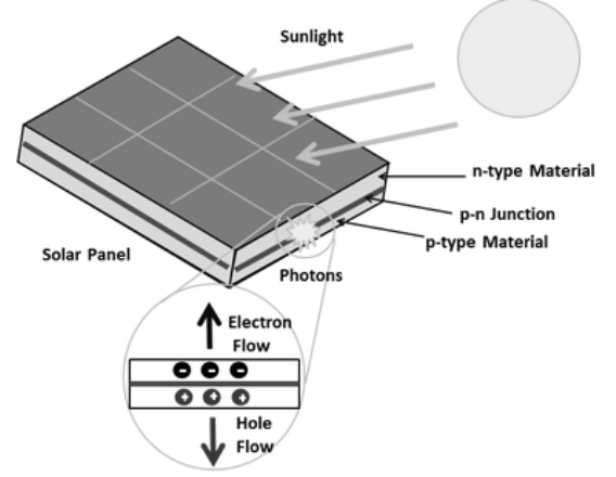 |
Figure 24: Solar Cell
The solar cell is composed of two layers which are struck together. The first layer is loaded with electrons, so these electrons are ready to jump from the first layer to the second layer. The second layer has some electrons taken away, and therefore, it is ready to take more electrons.
The advantages of solar cells are that, there is no fuel supply and cost problem. These are very dependable and require little maintenance.
A key issue with solar cells is conversion efficiency—convening the maximum amount of available solar energy into electrical energy. The higher the efficiency of the cells, the lower the cost and collection area required to achieve a desired electrical output.
A number of factors enter into the overall efficiency exhibited by a cell and involve both material and design considerations. Any discussion of conversion efficiency logically begins with the output from the sun.
Given a specific semiconductor material, it is the task to design and fabricate the solar cell to minimize further energy losses. In discussing device-related loss mechanisms, we will refer to the high-efficiency Si solar cell pictured in Figure 25.
Observe first of all that the contact to the top (light-incident) side of the cell is made through narrow "fingers." The fingers, all connected together along one edge of the cell are a design compromise. Zero-width fingers or fingers only along the cell edges would allow maximum light penetration to the underlying silicon. However, a series resistance of only a few ohms can seriously degrade the efficiency of a solar cell. The farther apart the fingers, the longer the current path through the narrow n-region at the top of the cell, and the greater the series resistance. Metallization and contact resistances can become important if the fingers are too narrow. The chosen finger size and spacing are calculated to provide an optimum trade-off between residual "shadowing," blocking of some of the light that strikes the cell, and cell series resistance.
Another potentially significant loss mechanism is the reflection of light at the Si surface. Approximately 30% of the light striking a bare planar Si surface at normal incidence will be reflected. To minimize losses due to reflection, the top surface of solar cells is typically "textured" and covered with an antireflection coating. Texturing of the surface, the formation of the inverted pyramids in decreases the reflected light by forcing the light to strike the Si surface two or more times before escaping.
Texturing is achieved by placing the Si in an anisotropic etching solution, an etch that preferentially removes Si atoms along certain crystalline planes. Having an index of refraction intermediate between air and Si, the topSiO2layer in the pictured cell, or preferably a deposited antireflection coating with optimized parameters, further reduces the reflection.
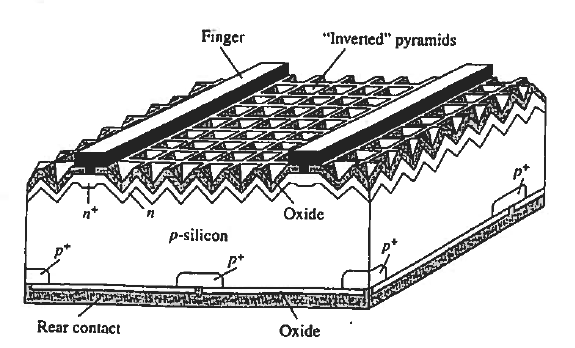 |
Figure 25: Solar Cell
Solar cells constructed in the described manner have attained a net reflection of less than 1%. Once the light has entered the semiconductor, the focus shifts to maximizing the light absorption.
In the Figure 25 solar cell the bottom surface oxide and metallization effectively form a mirror that reflects light hack into the silicon. Long wavelength light literally1 bounces back and forth between the top and bottom surfaces of the cell. This "light trap-ping" dramatically enhances the long (λ— λG) wavelength absorption.
Finally, the cell must be designed and built to collect as many of the photogenerated minority carriers as possible. This necessitates minimizing carrier recombination through-out the device structure.
Very long minority carrier lifetimes are the rule in modern single-crystal Si cells, yielding diffusion lengths greater than the width of the cell. With the top and bottom surfaces also carefully oxidized to minimize surface recombination, carriers generated almost anywhere in the cell volume have a high probability of diffusing to the depletion region and being swept to the opposite side of the junction before they recombine.
Solar Cell Basics
A variety of device structures have been employed in constructing solar cells. By far and away the most common cells are in essence just large-area pn junction photodiodes. Solar cells are designed of course to minimize energy losses, whereas photodiodes arc routinely designed to achieve a specific spectral response or a rapid time response.
Although there is design differences butI—V characteristics of solar cell are of the same general form as the photodiode characteristics.
We know that power is derived from the illuminated device if the d.c. Operating point lies in the fourth quadrant where I is negative and V is positive. Fourth-quadrant operation can be achieved in case of solar cell just by simply placing a resistor in series with the illuminated solar cell.
The fourth-quadrant characteristic is of prime interest in evaluating and applying solar cells. It is therefore common practice to show only the fourth-quadrant portion of the characteristics and to orient the — I axis upward on the plot as illustrated in Figure 26.
Figure 26 also graphically defines the following solar cell parameters of interest:
Voc - the open circuit voltage
Isc- the short circuit current
Vm Im - the operating point voltage and current yielding the maximum power output.
Vocis obviously the maximum voltage that can be supplied by the cell for a given photoinput,
Is, is the maximum current that can be derived from the cell.
It follows that Pmax= Vm Im<VocIsc
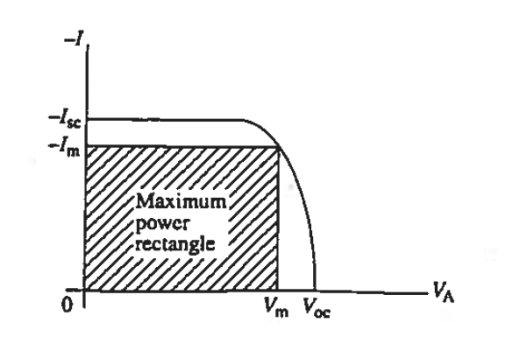 |
Figure 26: Inserted fourth-quadrant I—V characteristic of a solar cell under illumination with key solar cell parameters identified along the coordinate axes.
In calculations of solar cell performance, one often encounters
 |
FF is known as the fill factor and is of course always less than unity.
The ultimate measure of solar cell performance, the power conversion efficiency (n), is determined from the current-voltage parameters employing
 |
Where Pin, is the photo-energy incident per second or input power.
Key Takeaways
- A solar cell or photo-voltaic cell is an electronic device that directly converts sun’s energy into electricity.
- When sunlight falls on a solar cell, it produces both a current and a voltage to produce electric power.
- The advantages of solar cells are that, there is no fuel supply and cost problem. These are very dependable and require little maintenance.
- The higher the efficiency of the cells, the lower the cost and collection area required to achieve a desired electrical output.
- In calculations of solar cell performance, one often encounters fill factor FF is given by
 |
LED or Light emitting diode
Light emitting diode is a pn junction device. It is always operated in forward biased condition. LED converts electrical energy into light energy.
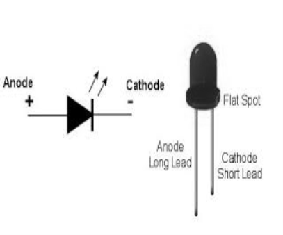 |
Figure 27: LED
Device Structure:
The LED structure plays a crucial role in emitting light from the LED surface. The LEDs are structured to ensure most of the recombination takes place on the surface by the following two ways.
- By increasing the doping concentration of the substrate, so that additional free minority charge carrier’s electrons move to the top, recombine and emit light at the surface.
- By increasing the diffusion length L =√Dτ, where D is the diffusion coefficient and τ is the carrier life time.
But when increased beyond a critical length there is a chance of reabsorption of the photons into the device. The LED has to be structured so that the photons generated from the device are emitted without being reabsorbed.
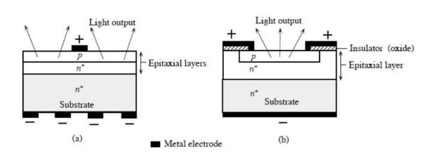 |
Figure 28: A schematic illustration of typical planar surface emitting LED devices. (a) p-layer grown epitaxially on an n+ substrate. (b) First n+ is epitaxially grown and then p region is formed by dopant diffusion into the epitaxial layer.
One solution is to make the p layer on the top thin, enough to create a depletion layer. Following picture shows the layered structure. There are different ways to structure the dome for efficient emitting
LEDs are usually built on an n-type substrate, with an electrode attached to the p-type layer deposited on its surface. P-type substrates, while less common, occur as well. Many commercial LEDs, especially GaN/InGaN, also use sapphire substrate.
In the fabrication of LED’s direct band gap semiconductors like GaP, GaAsP are used. In direct band gap semiconductors most of the energy is emitted in the form of light when hole and electron recombination takes place.
When an LED is forward biased the electrons and holes move in towards the junction and recombination takes place. As a result of recombination the electrons lying in the conduction band of an n- region fall into the holes lying in the valence band of a p –region. The difference of energy in the valence band and conduction band is radiated in the form of light energy. Here their excess energy is transferred to the emitted photon. The brightness of emitted light is directly proportional to the forward bias current.
Figures of Merit
A very important metric of an LED is the external quantum efficiency ηext. It quantifies the efficiency of the conversion of electrical energy into emitted optical energy.
Not all the photons emitted from the active region of an LED make it out of the device. Some are reabsorbed, some go in the wrong direction, some are reflected back. The light extraction efficiency of a LED is,
ηextraction 
The external quantum efficiency ext of a LED is, ηextraction 
|
It is defined as the light output divided by the electrical input power. It is also defined as the product of Internal radiative efficiency and Extraction efficiency. ηext = Pout(optical)/ IV
For indirect bandgap semiconductors ηext is generally less than 1%, whereas for a direct band gap material it could be substantial.
ηint = rate of radiation recombination/ Total recombination
The internal efficiency is a function of the quality of the material and the structure and composition of the layer.
LED materials
LEDs are comprised of compound semiconductor materials, which are made up of elements from group III and group V of the periodic table (these are known as III-V materials). Examples of III-V materials commonly used to make LEDs are gallium arsenide (GaAs) and gallium phosphide (GaP).
Ternary alloys based on alloying GaAs and GaP which are denoted by GaAs1-yPy. Inga Alp is an example of a quaternary (four elements) III-V alloy with a direct band gap. The LEDs realized using two differently doped semiconductors that are the same material is called a homojunction. When they are realized using different bandgap materials they are called a heterostructure device. A heterostructure LED is brighter than a homoJunction LED.
The main semiconductor materials used to manufacture LEDs are:
- Indium gallium nitride (InGaN): blue, green and ultraviolet high-brightness LEDs
- Aluminium gallium indium phosphide (AlGaInP): yellow, orange and red high-brightness LEDs
- Aluminium gallium arsenide (AlGaAs): red and infrared LEDs
- Gallium phosphide (GaP): yellow and green LEDs
Characteristics of LED
LEDs are solid-state devices. The advantages are:
1) Light Generated by LED is Directional
2) LED can Generate Different Light Colour
3) Temperature will Affect LED Efficacy
4) Low Energy Consumption
5) Long Life
The usage of LED is advantageous as it consumes less power and produces less heat. LEDs last longer than incandescent lamps.
Applications LEDs are used in
- For instrument display
- In calculators
- Digital clocks
- For indicating power ON/ OFF
- For optical switching application
- In optical communication system
- Medical devices
Key Takeaways
- Light emitting diode is a pn junction device. It is always operated in forward biased condition. LED converts electrical energy into light energy.
- When an LED is forward biased the electrons and holes move in towards the junction and recombination takes place.
- The light extraction efficiency of a LED is,
ηextraction  |
- LEDs are comprised of compound semiconductor materials, which are made up of elements from group III and group V of the periodic table (these are known as III-V materials). Examples of III-V materials commonly used to make LEDs are gallium arsenide (GaAs) and gallium phosphide (GaP).
It is a solid-state semiconductor laser. It is specifically fabricated p-n junction diode. This diode emits laser light when it is forward biased. A semiconductor laser is a device that causes laser oscillation by flowing an electric current to semiconductor. The mechanism of light emission is the same as a light-emitting diode (LED). Light is generated by flowing the forward current to a p-n junction. In forward bias operation, the p-type layer is connected with the positive terminal and the n-type layer is connected with the negative terminal, electrons enter from the n-type layer and holes from the p-type layer. When the two meet at the junction, an electron drops into a hole and light is emitted at the time.
We know that Laser radiation is highly monochromatic and it produces highly directional beams of light. In similar manner Semiconductor lasers works just like any other solid-state lasers and gas laser. The emitted radiation has spatial and temporal coherence. In spite of this similarity semiconductor lasers differ from other lasers in several important respects:
- In case of conventional lasers, the quantum transitions occur between discrete energy levels, whereas in case of semiconductor lasers the transitions are associated with the band properties of materials.
- Size of semiconductor laser is very compact almost of the order of 0.1mm long this is because the active region is very narrow of the order of 1μm thick or less, the divergence of the semiconductor laser beam is considerably larger than in case of conventional laser.
- The spatial and spectral characteristics of a semiconductor laser are strongly influenced by the properties of the junction medium (such as band gap and refractive index variations).
- For the p-n junction laser, the laser action is produced by simply passing a forward current through the diode itself. The result is a very efficient overall system that can be modulated easily by modulating the current. Since semiconductor lasers have very short photon lifetimes, modulation at high frequencies can be achieved.
Semiconductor laser is one of the most important light sources for optical-fiber communication because of its compact size and capability for high-frequency modulation.
Semiconductor Materials
All the lasing semiconductors have direct bandgaps. This is expected since the radiative transition in a direct bandgap semiconductor is a first-order process. Which implies that the momentum is automatically conserved. The transition probability is high.
For indirect bandgap semiconductors, the radiative transition is a second-order process that simply means it involves phonons or other scattering agents to conserve momentum and energy. Thus the radiative transition is much weaker.
Figure shows the range of laser emission wavelengths for various semiconductors from near ultraviolet to far infrared.
GaAs was the first material to lase, and its related III—V solid solutions have been most extensively studied and developed.
The IV—VI compounds, such as PbS, PbTe, PbSe, and related solid solutions, also exhibit laser action. They are direct bandgap materials with their extrema located along the (1 1 1) directions in the Brillouin zone, in contrast to GaAs with extrema located at the zone center.
In this section, we consider basic laser physics and use examples mainly from devices of III—V compound semiconductors. When compound semiconductors are formed that have more than one group III element distributed randomly on group III lattice sites or more than one group V element distributed randomly on group V lattice sites, these compounds are crystalline solid solutions.
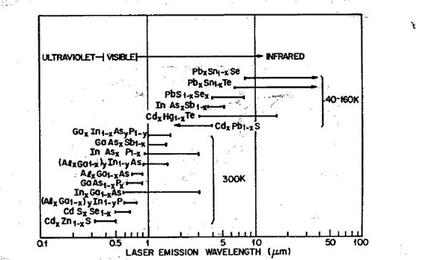 |
Figure 29: shows the range of laser emission wavelengths for various
The notation frequently used is AxB1-xCy for ternary and AxB1-xCyD1-yfor quaternary compounds, where A
And B are the group III elements and C and D are the group V elements.
The two most important Ill—V compound systems are AIxGa1-xAsySb1-y and GaxIn1-xAsyP1-y, solid solutions.
To achieve hetero structures with negligible interface traps, the lattices between the two semiconductors must be closely matched. The list of semiconductor materials that have exhibited laser action has continued to grow.
Semiconductor lasers require, for the active medium, a direct gap material and accordingly, the normal elemental semiconductors like Si or Ge cannot be used. The majority of semiconductor-laser materials are based on a combination of elements belonging to the third group of the periodic table such as Al, Ga, In with elements of the fifth group such as N, P,As, Sb. Examples include the best known GaAs as well as some ternary AlGaAs, InGaAs and quaternary InGaAsP alloys.
InGaN semiconductor lasers the best candidates for semiconductor laser emission in the very important blue-green spectral region. Semiconductor laser materials are not limited to III–V compounds, however. For the blue-green end of the spectrum we note that there are wide-gap semiconductors using a combination between elements of the second group (such as Cd and Zn) and of the sixth group (S, Se).
Double Heterostructure Laser
Figure 30 shows the basic structure of a p-n junction laser. Pair of parallel planes are cleaved or polished perpendicular to the plane of the junction. The two remaining sides of the diode are roughened to eliminate lasing in directions other than the main one. The structure is called a Fabry-Perot cavity.
When a forward bias is applied to the laser diode, a current flows. Initially at low current, there is spontaneous emission in all directions. As the bias is increased, eventually a threshold current is reached at which the stimulated emission occurs and a monochromatic and highly directional beam of light is emitted from the junction (Figure 30).
For the homostructure (e.g., GaAs p-n junction), the threshold current density increases rapidly with increasing temperature. A typical value of Jth (obtained by pulse measurement) is about 5.0 x 10⁴ A/cm2 at room temperature. Such a large current density imposes serious difficulties in operating the laser continuously at 300K. To reduce the threshold current density, heterostructure lasers have beenproposed and built using epitaxial technique.
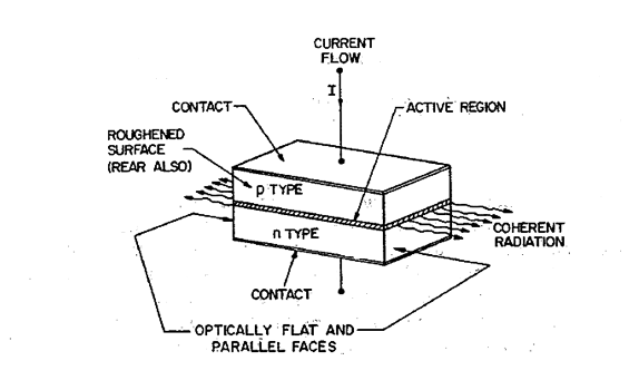 |
Figure 30: Structure of junction laser in the form of Fabry Perot Cavity
Semiconductor lasers represent one of the most important class of lasers in use today, not only because of the large variety of direct applications in which they are involved but also because they have found a widespread use as pumps for solid state lasers.
Key Takeaways
- It is a solid state semiconductor laser. It is specifically fabricated p-n junction diode. This diode emits laser light when it is forward biased. A semiconductor laser is a device that causes laser oscillation by flowing an electric current to semiconductor. The mechanism of light emission is the same as a light-emitting
- The two most important Ill—V compound systems are AIxGa1-xAsySb1-y and GaxIn1-xAsyP1-y, solid solutions.
- The basic structure of a p-n junction laser.is called a Fabry-Perot cavity.
- For the homostructure (e.g., GaAs p-n junction), the threshold current density increases rapidly with increasing temperature
References
- Semiconductor Device Fundamentals by Robert F. Pierret
- Physics of Semiconductor Devices by S.M. Sze.
- Electronic and optoelectronic properties of Semiconductor Structures by Jasprit Singh.