Unit - 1
DSP Preliminaries
The sampling theorem, which is also called as Nyquist theorem, delivers the theory of sufficient sample rate in terms of bandwidth for the class of functions that are bandlimited.
The sampling theorem states that, “a signal can be exactly reproduced if it is sampled at the rate fs which is greater than twice the maximum frequency W.”
Let us consider a band-limited signal, i.e., a signal whose value is non-zero between some –W and W Hertz.
Such a signal is represented as x(f)=0 for ∣f∣>W
For the continuous-time signal x (t), the band-limited signal in frequency domain, can be represented as shown in the following figure.
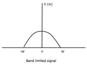
Fig 1 Band Limited Signal
If the signal x(t) is sampled above the Nyquist rate, the original signal can be recovered, and if it is sampled below the Nyquist rate, the signal cannot be recovered.
The following figure explains a signal, if sampled at a higher rate than 2w in the frequency domain.
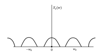
Fig 2 FT of xs(t)
The above figure shows the Fourier transform of a signal xs (t).
If fs<2W
The resultant pattern will look like the following figure.
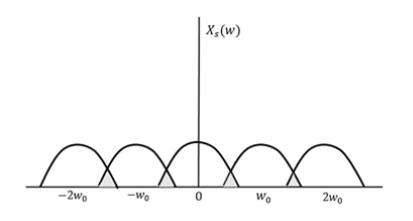
Fig 3 Resultant Signal
Here, the over-lapping of information is done, which leads to mixing up and loss of information. This unwanted phenomenon of over-lapping is called as Aliasing.
Aliasing
Aliasing can be referred to as “the phenomenon of a high-frequency component in the spectrum of a signal, taking on the identity of a low-frequency component in the spectrum of its sampled version.”
Key takeaway
The sampling theorem, which is also called as Nyquist theorem, delivers the theory of sufficient sample rate in terms of bandwidth for the class of functions that are bandlimited.
Fs<2fm
Numerical:
1. The continuous-time signal x(t) = cos(200πt) is used as the input for a CD converter with the sampling period 1/300 sec. Determine the resultant discrete-time signal x[n].
Solution:
We know,
X[n] =x(nT)
= cos(200πnT)
= cos(2πn/3) , where n= -1,0,1,2……
The frequency in x(t) is 200π rad/s while that of x[n] is 2π/3.
2. Determine the Nyquist frequency and Nyquist rate for the continuous-time signal x(t) which has the form of:
X(t) = 1+ sin(2000πt) + cos (4000πt)
Solution:
The frequencies are 0, 2000π and 4000π.
The Nyquist frequency is 4000π rad/s and the Nyquist rate is 8000π rad/s.
3. Consider an analog signal.

Solution.
The frequency in the analog signal

The largest frequency is

The Nyquist rate is

4. The analog signal

- What is the Nyquist rate for this signal?
- Using a sampling rate
 . What is discrete time signal obtained after sampling?
 - What is analog signal
 we can reconstruct from the samples if we use ideal interpolation?
Solution.
- The frequency of the analog signal are


2. For 


For  ,the folding frequency is
Hence  is not effected by aliasing
 Is changed by the aliasing effect
 Is changed by the aliasing effect
So that normalizing frequencies are

The analog signal that we can recover is

Which is different than the original signal 
5. 
- Find the minimum sampling rate required to avoid aliasing.
- If
 , what is the discrete time signal after sampling?
 - If
 , what is the discrete time signal after sampling?
 - What is the frequency F of a sinusoidal that yields sampling identical to obtained in part c?
Solution. a. 
The minimum sampling rate is

And the discrete time signal is

b. If  , the discrete time signal is

c. If Fs=75Hz , the discrete time signal is

d. For the sampling rate 
 in part in (c). Hence

So, the analog sinusoidal signal is


6. Suppose a continuous-time signal x(t) = cos (Ø0t) is sampled at a sampling frequency of 1000Hz to produce x[n]: x[n] = cos(πn/4)
Determine 2 possible positive values of Ø0, say, Ø1 and Ø2. Discuss if cos(Ø1t) or cos(Ø2t) will be obtained when passing through the DC converter.
Solution:
Taking T= 1/1000s
Cos(πn/4) =x[n] = x(nT) = cos (Ø0n/1000)
Ø1 is easily computed as 
Ø1 = 250π
Ø2 can be obtained by noting the periodicity of a sinusoid:
 Ø2n/1000)
Ø2 = 2250π
Reconstruction process
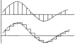
Fig 4 Sampled Data
The sampled data signal is modified by the controller. The hold circuit than converts the signal to analog form. The simplest hold circuit is ZOH (zero order hold) in which the reconstructed signal acquires the same value as the last received sample for the entire sampling period.
The process of transforming x[n] back to x(t) is recovery of signal. This can be done by
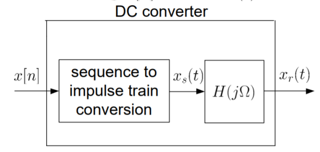
Fig 5 Block diagram
Let H(j) is


To get h(t) , we take inverse Fourier transform of H(j )
)

Where 


The interpolation formula can be verified at t=nT


For n=k, we use L’ Hopital’s rule to obtain:


Example
Suppose a continuous-time signal x(t)= cos( 0t) is sampled at a sampling frequency of 1000Hz to produce x[n]

Determine two possible positive values of  0 .
0 .
Sol: From sampling we know that T=1/1000s


 can be obtained by nothing the periodicity of a sinusoid:

As a result we have

A complex exponential signal, whether in continuous time or in discrete time, is completely determined by its amplitude A, phase α, and frequency which can be F0 Hz (or Ω0 rad/sec) in continuous time or w0 radians in discrete time, as in the following expressions:
X(t) =A ejα ejΩ0t = A ejα ej2πF0t
X[n] = A ejα ejw0n
When the signal is the superposition (ie sum) of two or more complex exponentials of different amplitudes and phases, we just add them in the plot and place them appropriately in frequency. So for example a sinusoidal signal, as
X(t) = A+ cos(2π F0t + α)
= (A/2) ejα ej2πF0t + (A/2) e-jα e-j2πF0t
Is represented by two complex exponentials with frequencies F0 and -F0 respectively, as shown in figure. Notice the appearance of the negative frequency -F0 which corresponds to the complex exponential with the same amplitude and opposite phase.
Similarly for the discrete time case.
A discrete time sinusoid
X[n] = A cos(w0n +α) = (A/2) ejα ejw0n + (A/2) e-jα e-jw0n
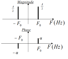
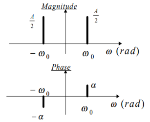
Fig 6 Frequency and Phase Response
The process of sampling rate conversion in the digital d om ain can be view ed as a linear filtering operation, as illustrated in Fig below. The input signal x(n) is characterized by the sampling rate Fx = 1/Tx and the output signal y(m) is characterized by the sampling rate Fv = 1/Ty, where Tx an d Ty are the corresponding sampling intervals. In the m ain p a rt of our treatment, the ratio Fy/Fx is constrained to be rational,
Fy/Fx =I/D
w here D and I are relatively prim e integers. We shall show that the linear filter is characterized by a time-variant im pulse response, denoted as h(n,m). Hence the input x(n) and the output v(m) are related by the co n volution summation for time-variant systems.
The sampling rate conversion can be determined by the digital resampling of the same analog signal. If x(t) is the analog signal that is sampled at the first rate Fx so that we obtain x(n). The main aim is to directly determine the sequence y(m) directly from x(n) which is the sampled value of x(t) at s second rate Fy.
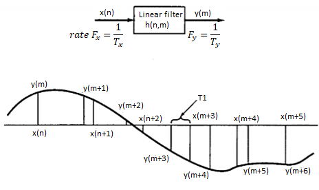
Fig 7 Sampling Rate Conversion
Decimation
Decimation, or down-sampling, consists of reducing the sampling rate by a factor M, cf. Figure. Here, the output is defined as

Fig 8 Decimation by factor M
y(m) = x(mM)
i.e., it consists of every Mth element of the input signal. It is clear that the decimated signal y does not in general contain all information about the original signal x. Therefore, decimation is usually applied in filter banks and preceded by filters which extract the relevant frequency bands.
In order to analyze the frequency domain characteristics of a multirate processing system with decimation, we need to study the relation between the Fourier transforms, or the z-transforms, of the signals x and y. For simplicity we consider the case M = 2 only. Then the decimated signal y is given by
y(m) = x(2m)
 given the z-transforms of

z-transform of y(m) is given by


For finding the z-transform of y decimation is done in two stages as shown below

The above signal has z-transform as


The Fourier transform of the decimated signal y(m) is related to z-transform by

But 

Where X is the Fourier-transform of the sequence {x(n)}. But from the properties of the Fourier transform (periodicity and symmetry) it follows that X(ω/2 + π) = X(ω/2 − π) = X(π − ω/2)∗ . Hence

The Fourier-transform of {y(m)} thus cannot distinguish between the frequencies ω/2 and π − ω/2 of {x(n)}. This is equivalent to the frequency folding phenomenon occurring when sampling a continuous-time signal. Hence, whereas the signal {x(n)} consists of frequencies in [0, π], the frequency contents of the decimated signal {y(m)} are restricted to the range [0, π/2]. Moreover, after decimation of the signal {x(n)}, its frequency components in [0, π/2] cannot be distinguished from the frequency components in the range [π/2, π].
Interpolation
Expansion, or up-sampling, consists of increasing the sampling rate by a factor L, cf. Figure below. Here, the output is obtained by inserting L-1 zeros between successive values of the input x(n)


Fig 9 Interpolation by factor L
The expansion operation followed by interpolation leads to a representation of the signal x at a sampling rate increased by the factor L. The expanded signal {y(m)} has the z-transform

The Fourier Transform is

The transform Y (ω) at a given frequency ω ∈ [0, π] is thus equal to X(ωL), where ωL ∈ [0, Lπ]. But as the Fourier-transform is periodic with period 2π, we have X(ωL) = X(ωL + 2πk) = X((ω + 2πk L )L), and it follows that Y (ω) = Y (ω + 2πk L ). Hence Y (ω) is periodic, with L repetitions of X(ω) in the frequency range [0, 2π]. For example, for L = 2, we have X(2ω) = X(2ω − 2π) = X(2π − 2ω) ∗ = X(2(π − ω))∗ . Hence, for L = 2,

And Y (ω) is therefore uniquely defined by its values in the frequency band [0, π/2]. In order to reconstruct the correct interpolating signal at the higher sampling rate, an interpolating filter has to be introduced after the expansion. This is equivalent to the situation in D/A conversion, where a low-pass filter is used after the hold function.
Key takeaway
The set of filters used to reconstruct the desired signal is called synthesis filter bank.
Orthogonality
Let us consider a set of n mutually orthogonal functions x1(t), x2(t)... xn(t) over the interval t1 to t2. As these functions are orthogonal to each other, any two signals xj(t), xk(t) have to satisfy the orthogonality condition. i.e.


Let a function f(t), it can be approximated with this orthogonal signal space by adding the components along mutually orthogonal signals i.e.


If  are two complex functions, then
  can be expressed in terms of
  as
as
 , with negligible error
Where, 
Where,  c0mplex conjugate of
If  are orthogonal then


Basis Function
- Basic idea: If a signal can be represented by n-tuple then it can be treated in much the same way as a n-dim vector.
- Let  be n signal.
- Consider a signal x(t) and suppose that

- If every signal can be written as above
 basic function
- Signal set  is an orthogonal set if

-  is an orthonormal set
- 


Numerical:
Consider the following signal set:

Solution:
By inspection, the signals can be expressed in terms of the following two basis functions:


Note that the basis is orthogonal

Also note that each these functions have unit energy

We say that they form an orthonormal basis.

Fig 10 Block Diagram of DSP
To perform the processing digitally, there is a need for an interface between the analog signal and the digital processor. This interface is called an analog-to-digital (A/D) converter. The output of the AD converter is a digital signal that is appropriate as an input to the digital processor.
The digital signal processor may be a large programmable digital computer or a small microprocessor programmed to perform the desired operations on the input signal. It may also be a hardwired digital processor configured to perform a specified set of operations on the input signal.
Programmable machines provide the flexibility to change the signal processing operations through a change in the software, whereas hardwired machines are difficult to reconfigure. Consequently, programmable signal processors are in very common use.
On the other hand, when signal processing operations are well defined, a hardwired implementation of the operations can be optimized, resulting in a cheaper signal processor and, usually, one that runs faster than its programmable counterpart.
In applications where the digital output from the digital signal processor is to be given to the user in analog form, such as in speech communications, we must provide another interface from the digital domain to analog domain. Such an interface is called a digital-to-analog (D/A) converter. Thus the signal is provided to the user in analog form.
However, there are other practical applications involving signal analysis, where the desired information is conveyed in digital form and no D/A converter is required. For example, in the digital processing of radar signals, the information extracted from the radar signal, such as the position of the aircraft and its speed, may simply be printed on paper. There is no need for a D/A converter in this case.
Key takeaway
The digital signal processor may be a large programmable digital computer or a small microprocessor programmed to perform the desired operations on the input signal. It may also be a hardwired digital processor configured to perform a specified set of operations on the input signal.
1. Physical size of analog systems is quite large while digital processors are more compact and light in weight.
2. Analog systems are less accurate because of component tolerance ex R, L, C and active components. Digital components are less sensitive to the environmental changes, noise and disturbances.
3. Digital system is most flexible as software programs & control programs can be easily modified.
4. Digital signal can be stores on digital hard disk, floppy disk or magnetic tapes. Hence becomes transportable. Thus easy and lasting storage capacity.
5. Digital processing can be done offline.
6. Mathematical signal processing algorithm can be routinely implemented on digital signal processing systems. Digital controllers are capable of performing complex computation with constant accuracy at high speed.
7. Digital signal processing systems are upgradeable since that are software controlled.
8. Possibility of sharing DSP processor between several tasks.
9. The cost of microprocessors, controllers and DSP processors are continuously going down. For some complex control functions, it is not practically feasible to construct analog controllers.
10. Single chip microprocessors, controllers and DSP processors are more versatile and powerful.
The TMS320C6x are the first processors to use velocity architecture, having implemented the VLIW architecture. The TMS320C62x is a 16-bit fixed point processor and the ‘67x is a floating point processor, with 32-bit integer support
The C6713 DSK is a low-cost standalone development platform that enables users to evaluate and develop applications for the TI C67xx DSP family. The DSK also serves as a hardware reference design for the TMS320C6713 DSP. Schematics, logic equations and application notes are available to ease hardware development and reduce time to market.
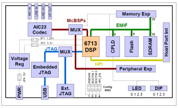
Fig 11 Block Diagram of Processor
Features
- The DSK comes with a full compliment of on-board devices that suit a wide variety of application environments. Key features include
- A Texas Instruments TMS320C6713 DSP operating at 225 MHz.
- An AIC23 stereo codec
- 16 Mbytes of synchronous DRAM
- 512 Kbytes of non-volatile Flash memory (256 Kbytes usable in default configuration)
- 4 user accessible LEDs and DIP switches
- Software board configuration through registers implemented in CPLD
- Configurable boot options
- Standard expansion connectors for daughter card use
- JTAG emulation through on-board JTAG emulator with USB host
- Interface or external emulator
- Single voltage power supply (+5V)
Architecture
The simplified architecture of TMS320C6713 is shown in the Figure below. The processor consists of three main parts: CPU, peripherals and memory.
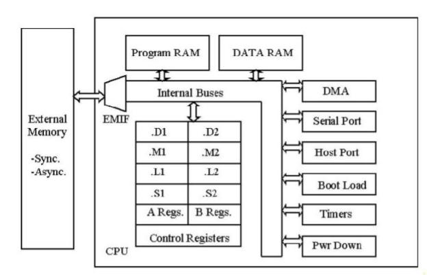
Fig 12 Architecture
Central Processing Unit
The CPU contains program fetch unit, Instruction dispatch unit, instruction decode unit. The CPU fetches advanced very-long instruction words (VLIW) (256 bits wide) to supply up to eight 32-bit instructions to the eight functional units during every clock cycle. The VLIW architecture features controls by which all eight units do not have to be supplied with instructions if they are not ready to execute. The first bit of every 32-bit instruction determines if the next instruction belongs to the same execute packet as the previous instruction, or whether it should be executed in the following clock as a part of the next execute packet. Fetch packets are always 256 bits wide; however, the execute packets can vary in size. The variable-length execute packets are a key memory-saving feature, distinguishing the C67x CPU from other VLIW architectures. The CPU also contains two data paths (Containing registers A and B respectively) in which the processing takes place. Each data path has four functional units (.L, .M, .S and .D).
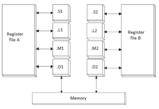
Fig 13 Simplified Block Diagram of Data Path
All instructions except loads and stores operate on the register. All data transfers between the register files and memory take place only through two data-addressing units (.D1 and .D2). The CPU also has various control registers, control logic and test, emulation and logic. Access to control registers is provided from data path B.
The CPU contains two general purpose register files A and B. These can be used for data or as data address pointers. Each file contains sixteen 32-bit registers (A0-A15 for file A and B0- B15 for file B). The registers A1, A2, B0, B1, B2 can also be used as condition registers. The registers A4-A7 and B4-B7 can be used for circular addressing. These registers provide 32-bit and 40-bit fixed-point data. The 32-bit data can be stored in any register. For 40-bit data, processor stores least significant 32 bits in an even register and remaining 8 bits in upper (odd) register.
The CPU features two sets of functional units. Each set contains four units and a register file. One set contains functional units .L1, .S1, .M1, and .D1; the other set contains units .D2, .M2, .S2, and .L2. The two register files each contain sixteen 32-bit registers for a total of 32 general-purpose registers. The two sets of functional units, along with two register files, compose sides A and B of the CPU. Each functional unit has two 32-bit read ports for source operands and one 32-bit write port into a general purpose register file. The functional units . L1, .S1, .M1, and .D1 write to register file A and the functional units .L2, .S2, .M2, and .D2 write to register file B. As each unit has its own 32-bit write port, all eight ports can be used in parallel in every cycle. The .L, .S, and .M functional units are ALUs. They perform 32-bit/40-bit arithmetic and logical operations. .S unit also performs branching operations and .D units perform linear and circular address calculations. Only .S2 unit performs accesses to control register file.
The memory system of the TMS320C671x series processor implements a modified Harvard architecture, providing separate address spaces for instruction and data memory. The processor uses a two-level cache-based architecture and has a powerful and diverse set of peripherals. The Level 1 program cache (L1P) is a 4K-byte direct-mapped cache and the Level 1 data cache (L1D) is a 4K-byte 2-way set-associative cache. The Level 2 memory/cache (L2) consists of a 256K-byte memory space that is shared between program and data space. 64K bytes of the 256K bytes in L2 memory can be configured as mapped memory, cache, or combinations of the two. The remaining 192K bytes in L2 serve as mapped SRAM.
Key takeaway
The C6713 DSK is a low-cost standalone development platform that enables users to evaluate and develop applications for the TI C67xx DSP family. The DSK also serves as a hardware reference design for the TMS320C6713 DSP. Schematics, logic equations and application notes are available to ease hardware development and reduce time to market
References:
1. Ifeachor E.C, Jervis B. W, “Digital Signal Processing: Practical approach”, Pearson Publication, 2nd Edition.
2. Li Tan, “Digital Signal Processing: Fundamentals and Applications”, Academic Press, 3rd Edition.
3. Schaum's Outline of “Theory and Problems of Digital Signal Processing”, 2nd Edition.
4. Oppenheim, Schafer, “Discrete-time Signal Processing”, Pearson Education, 1st Edition.
5. K.A. Navas, R. Jayadevan, “Lab Primer through MATLAB”, PHI, Eastern Economy Edition.