Unit - 1
Study of Power Devices
- SCR is a solid state-operated device with the four-layered structure. The flow of current is in one direction just like a diode.
- It has three junctions along with the three terminals. The other name for SCR is Thyristor. These are the devices that are operated with the current.
- A large value of the current at the anode terminal is controlled by the value of the current applied at the terminal gate. Hence these are known as current-controlled devices.
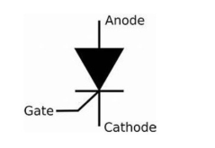
Figure 1. Symbolic Representation of SCR
- An SCR is constructed with four layers that consist of P-type and N-type semiconductor material. These are layered in such a way that it tends to form three junctions J1, J2, and J3. The three terminals that are attached to it are known as anode, cathode, and gate.
- The anode is the basic terminal through which the current flows or enters the device. The cathode is the terminal through which the entered current leaves the device.
- The current entering terminal is of positive polarity and the terminal through which the current is leaving is of negative polarity. In between the flow of current among the terminals, there must be a terminal that can provide the control. This can be provided by the terminal gate. This terminal is sometimes also referred to as the terminal of control.
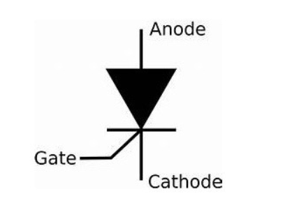
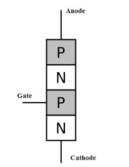
Figure 2. PNPN Type SCR
- Consider SCR of P-N-P-N type. In this structure the anode is connected at the above that is to P-type and the cathode is connected at the end that is for N-type , whereas the gate is connected to the p-type but it will be the second P-type in the sequence. Hence the gate terminal is positioned in such a way that it is nearer to the terminal cathode.
- In this, the junction J1 is formed in between the first P-type and the N-type. The second junction J2 will be lying in between N-type and the second P-type layers. The third junction will be in between the last P-type and the N-type layers. Based on the requirement or the necessity of the applications these layers of the Thyristor are doped. Silicon is preferred since it is intrinsic type.
Working:
- SCR starts conducting when it is forward biased, for this purpose the cathode is kept negative and anode positive. When a positive clock pulse is applied at the gate SCR is turned ON.
- Under forward biased condition J1 and J3 are forward biased and J2 is reverse biased. When clock pulse is applied at gate terminal J2 is forward biased and SCR starts conducting.
- SCR turns OFF and ON quickly. At OFF state SCR provides infinite resistance and in the ON state it offers low resistance may be in the range of 0.01 Ω to 1Ω.
Key takeaways
An SCR is constructed with four layers that consist of P-type and N-type semiconductor material. These are layered in such a way that it tends to form three junctions J1, J2, and J3. The three terminals that are attached to it are known as anode, cathode, and gate.
Static Characteristic:
Figure 3 shows the circuit diagram to obtain V – I characteristic of the SCR.
Here VAK is voltage between anode to cathode and Vg is gate voltage.
The static V – I characteristic of the SCR is divided into following mode.
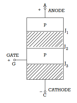
Figure 3. Circuit Diagram for V-I characteristics of SCR
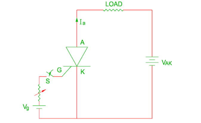
Figure 4. V-I characteristics of SCR
Reverse blocking mode
- When cathode is made positive with respect to anode and gate switch is kept open circuited, junction J1 and J3 are reverse biased whereas the junction J2 becomes forward biased.
- Hence only small leakage current flows through the device.
- If the anode voltage increases to certain level, an avalanche break down occurs at the junction J2 and current flows sharply through all the junctions.
- This current is limited to safe value to protect SCR due to high power dissipation.
- The region OA is known as forward blocking mode and AB is known as reverse avalanche breakdown mode of the SCR.
Forward blocking mode
- When anode is made positive with respect to cathode and switch S is kept open circuited, junction J1 and J3 are forward biased whereas the junction J2 become reverse biased.
- This will result in only small leakage current flows through the device.
Forward conducting mode
- When anode to cathode voltage increases to certain level say threshold voltage, an avalanche breakdown occurs at junction J2 and device comes into conduction state region PQ
- The voltage across SCR drops from several thousand voltage to few voltage and current increases sharply in the forward conducting state.
- When the gate signal is applied, SCR is turned on before forward break over voltage is reached.
- Higher the gate current, lower the forward break over voltage.
- Figure shows different value of gate current and corresponding break over voltage.
- Once the SCR conducts, it remains in conducting state despite gate signal removes.
- The SCR will turn off only when the forward current is reduced below holding current.
Dynamic characteristic
The switching action does not take place instantaneously, but it will take some finite time.
Turn on time (ton)
The turn on time of the SCR is defined as the time during which the SCR changes from forward blocking state to forward conducting state.
The total turn on time of the SCR is divided in to two intervals:
Delay time and Rise time
Ton = td + tr
Delay time (td)
It is time duration from the instant at which the gate current reaches 90% of its final value to the instant at which anode current reaches 10% of its final value.
Rise time (tr)
It is defined as time during which anode current rises from 10% to 90% of final value.
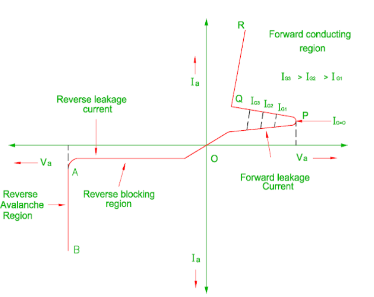
Figure 5. SCR turn on Waveforms
Turn off time (toff)
- Once the SCR start to conduct, gate loses control.
- The SCR can be turned off by reducing the anode current below holding current for sufficient time.
- This can be achieved by natural commutation or forced commutation.
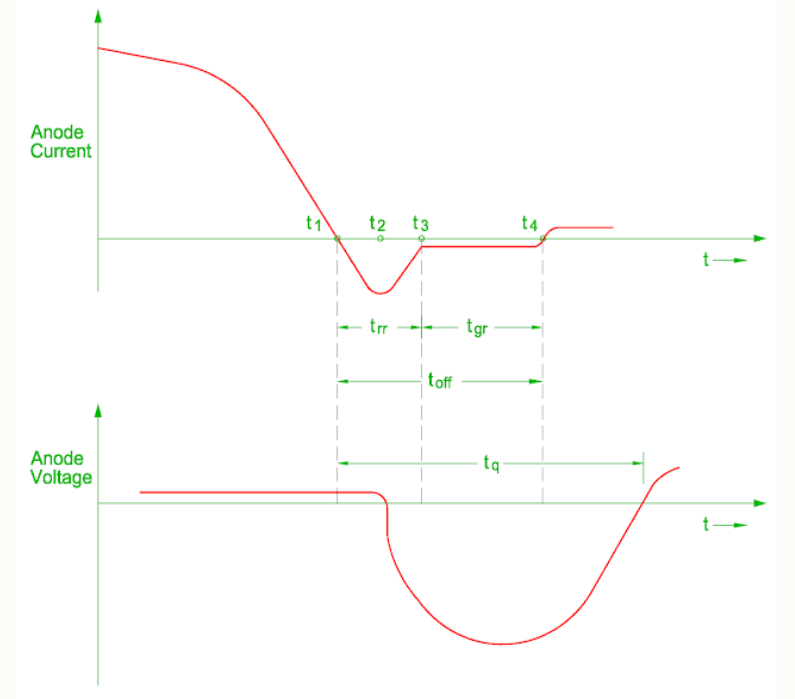
- The turn off time of the SCR is defined as the time interval between the instant at which the anode current becomes zero and the instant at which SCR regain forward blocking voltage.
The total turn off time can be divided in to two intervals:
Reverse recovery time ( trr ) and gate recovery time ( tgr )
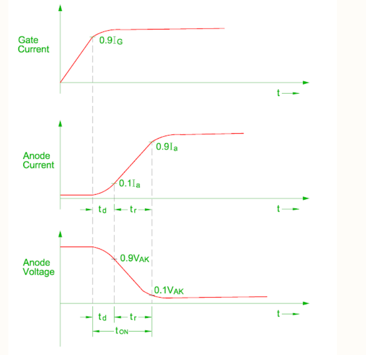
Figure 6. SCR turn-off waveforms
- The anode current becomes zero at instant t1.
- The anode current flows in the opposite direction during reverse recovery time t3 – t1.
- The reverse anode voltage developed across SCR at the instant t2 and reverse current continue to decrease.
- Therefore, the reverse recovery time is defined as the time between the current reversal and the instant at reverse current has decayed to 10% of negative peak value.
- The reverse recovery time increases as the forward current increases.
- When the reverse recovery current stops, high transient voltage appears across the SCR which may damage it.
- The middle junction J2 contains charges which must decay only by recombination at the end of reverse recovery time.
- This recombination is possible if a reverse voltage is maintained across the SCR therefore the time for recombination of charges ( t3 – t4 ) is called as gate recovery time tgr.
- The recombination is stopped at time t4 and forward voltage can be reapplied at time instant.
- The turn off time of the SCR is given is in the range of 3 to 100 micro- second.
- In practice circuit turn off time must be greater than SCR turn off time.
- Therefore, the circuit turn off time tc is defined as the time between the instant anode current becomes zero and at the instant reverse voltage becomes practically zero.
- The circuit turn off time tc must be greater than the SCR turn off time otherwise the SCR may turn on at undesired instant and it is known as commutation failure.
- The turn off time increases with increase in the magnitude of anode current and junction temperature.
- It also depends upon type of commutation circuit i.e. natural commutation or forced commutation.
Key takeaway
In dynamic characteristics: The turn on time of the SCR is defined as the time during which the SCR changes from forward blocking state to forward conducting state.
The total turn on time of the SCR is divided in to two intervals:
Delay time and Rise time
Ton = td + tr
Switching characteristics of SCR
Turn ON Time of SCR
- A forward biased thyristor can be turned on by applying a positive voltage between gate and cathode terminal.
- But it takes some transition time to go from forward blocking mode to forward conduction mode.
- This transition time is called turn on time of SCR
- It is subdivided into three small intervals as delay time (td) rise time(tr), spread time(ts).
Delay Time of SCR
When gate current is applied, the thyristor will start conducting over a very tiny region.
It can be defined as the time taken by the gate current to increase from 90% to 100% of its final value Ig.
Rise Time
- Rise time of SCR in the time taken by the anode current to rise from 10% to 90% of its final value. At the same time anode voltage will fall from 90% to 10% of its initial value Va.
- The phenomenon of decreasing anode voltage and increasing anode current is entirely dependent upon the type of the load.
Spread Time
- It is the time taken by the anode current to rise from 90% to 100% of its final value. At the same time the anode voltage decreases from 10% of its initial value to smallest possible value.
- In this interval of time conduction spreads all over the area of cathode and the SCR will go to fully ON State.
- Spread time of SCR depends upon the cross-sectional area of cathode.
Turn off time of SCR can be defined as the interval between anode current falls to zero and device regains its forward blocking mode.
On the basis of removing carrier charges from the four layers, turn off time of SCR can be divided into two time regions,
- Reverse Recovery Time.
- Gate Recovery Time
Reverse Recovery Time:
- It is the interval in which change carriers remove from J1, and J3 junction. At time t1, anode current falls to zero and it will continue to increase in reverse direction with same slope (di/dt) of the forward decreasing current.
- This negative current will help to sweep out the carrier charges from junction J1 and J3. At the time t2 carrier charge density is not sufficient to maintain the reverse current hence after t2 this negative current will start to decrease.
- The value of current at t2 is called reverse recovery current. Due to rapid decreasing of anode current, a reverse spike of voltage may appear across the SCR. Total recovery time t3 – t1 is called reverse recovery time.
Gate Recovery Time
- After sweeping out the carrier charges from junction J1 and J3 during reverse recovery time, there remain trapped charges in J2 junction that prevent the SCR from blocking the forward voltage.
- This trapped charge can be removed by recombination and the interval in which this recombination is done, called gate recovery time.
GTO (gate turn-off) is like thyristor. It is a four layer, three junction P-N-P-N device like a standard thyristor. In this, the n+ layer at the cathode end is highly doped to obtain high emitter efficiency.
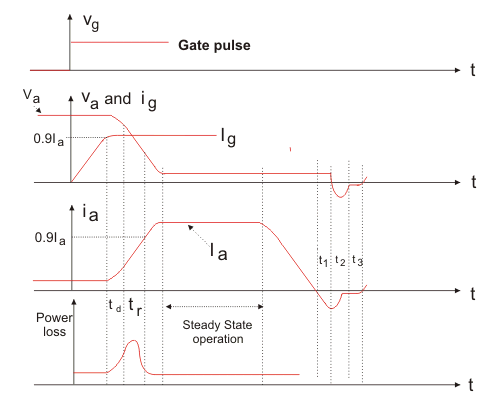
Figure 7. Symbol of GTO
Construction of GTO:
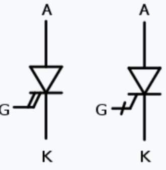
Figure 8. Structure of GTO
- Consider the structure of GTO which is similar to thyristor. It is a four layered structure which has three junctions P-N-P-N device. The n+ layer at the cathode end is highly doped to obtain high emitter efficiency.
- This results in the breakdown voltage of the junction J3 which I low and typically in the range of 20-40 volts.
- The doping level of p-type is highly graded because the doping level should be low to maintain high emitter efficiency whereas for having good turn OFF properties, doping of this region should be high.
- The gate and cathode should be highly interdigit with various geometric forms to optimize the current turn off capability.
- The junction between P+anode and N base is called anode junction.
- A heavily doped P+ anode region is required to obtain high efficiency anode junction so that good turn ON properties is achieved.
Principle of Operation:
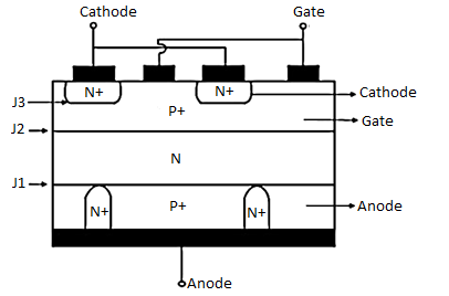
Figure 9. GTO operation
- When the anode terminal is made positive with respect to cathode by applying a positive gate current, the hole current injection from gate forward bias the cathode p-base junction.
- This results in the emission of electrons from the cathode towards the anode terminal. This induces the hole injection from the anode terminal into the base region. This injection of holes and electrons continuous till the GTO comes into the conduction state.
- To turn OFF a conducting GTO, a reverse bias is applied at the gate by making the gate negative with respect to cathode. A part of the holes from the P base layer is extracted through the gate which suppress the injection of electrons from the cathode.
- In response to this, more hole current is extracted through the gate results more suppression of electrons from the cathode. Eventually, the voltage drop across the p base junction causes to reverse bias the gate cathode junction and hence the GTO is turned OFF.
- During the hole extraction process, the p-base region is gradually depleted so that the conduction area squeezed. As this process continuous, the anode current flows through remote areas forming high current density filaments. This causes local hot spots which can damage the device unless these filaments are extinguished quickly.
- By the application of high negative gate voltage these filaments are extinguished rapidly. Due to the N base region stored charge, the anode to gate current continues to flow even though the cathode current is ceased.
- This is called a tail current which decays exponentially as the excess charge carriers are reduced by the recombination process. Once the tail current reduced to a leakage current level, the device retains its forward blocking characteristics.
V-I Characteristics
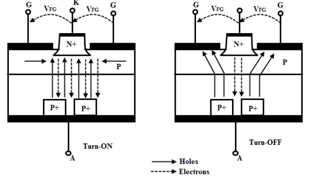
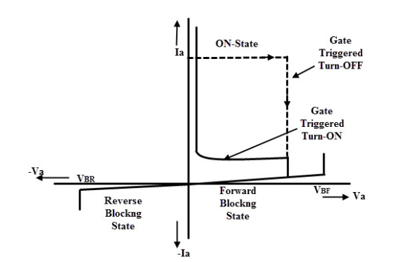
Figure 10. V-I characteristics of Thyristor
When the anode is made positive with respect to cathode, the device operates in forward blocking mode. By the application of positive gate signal triggers, the GTO into conduction state.
The latching current and forward leakage currents are considerably higher in GTO compared to the thyristor as shown in figure. The gate drive can be removed if the anode current is above the holding current level.
It is good not to remove the positive gate drive during conduction and to hold at value more than the maximum critical gate current
This causes the anode current dips below the holding current level transiently, which forces a high anode current at a high rate back into the GTO. This can be potentially destructive.
The GTO can be turned OFF by the application of reverse gate current which can be either step or ramp drive. The GTO can be turned OFF without reversing anode voltage. The dashed line in the figure shows i-v trajectory during the turn OFF for an inductive load.
To avoid dv/dt triggering and protect the device during turn OFF, either a recommended value of resistance must be connected between the gate and cathode or a small reverse bias voltage (typically -2V) must be maintained on the gate terminal. This prevents the gate cathode junction to become forward biased and hence the GTO sustains during the turn OFF state.
Applications:
- AC drives
- DC drives or DC choppers
- AC stabilizing power supplies
- DC circuit breakers
- Induction heating
- And other low power applications
Key takeaway
GTO (gate turn-off) is like thyristor. It is a four layer, three junction P-N-P-N device like a standard thyristor. In this, the n+ layer at the cathode end is highly doped to obtain high emitter efficiency.
| Thyristor | GTO |
Availability | Early 60s | Mid 80s |
Voltage Ratings | 5kV | 5kV |
Current Ratings | 4kA | 5kA |
Switching Frequencies | Low | 2kHz |
On-state voltage drop | 2V | 2-3V |
Drive circuit | Simple | Very difficult |
Comments | Cannot turn-off using gate signals | King in very high power |
Power Metal Oxide Semiconductor Field Effect Transistor
This device is capable of switching at a high frequency up to 100 kHz. that is higher than power BJT. It has a good current carrying capacity and higher off-state blocking voltage capacity. A power MOSFET is a voltage-controlled device.
Types of MOSFET
- Depletion type MOSFET
- Enhancement type MOSFET
Construction
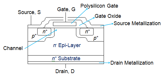
Power MOSFET has a vertically oriented four-layer structure.
- The p-type middle layer term as the body.
- The n– layer is the drift layer.
- This layer is lightly dropped as compared to the drain and source layer.
- The breakdown voltage of power MOSFET determines from the width of the drift layer.
- First and last both layers are an n+ layer. First layer is the source layer and the last layer is the drain layer.
The n+ p n- n+ structure term as enhancement mode n channel MOSFET.
A p-channel MOSFET structure has exactly opposite doping profile.
- The GATE terminal is not directly connected with p-type, there is an oxide layer between the metal and semiconductor.
- This oxide layer act as a dielectric layer between the metal and the semiconductor. It forms a MOS (metal oxide semiconductor) capacitance at the input of the MOSFET.
- This capacitance is large (>1000 pF). The oxide layer gives good insulating property by providing the SiO2 layer that isolates the gate terminal from the body layer.
Working Principle:
- Power MOSFET is a minority carrier device. So, conduction takes place by the presence of electrons.
- Therefore, the conduction cannot take place through the MOSFET from the drain to source due to the presence of P-layer in between. But this is possible by Inversion layer creation.
The operation of MOSFET divides into two parts
- Formation of the depletion layer
- Creation of Inversion Layer
Formation of the depletion layer
- When a positive voltage is connected to the drain with respect to the source and gate is positive with respect to the body, the MOSFET works as forward biased.
- The p-layer has a large number of holes and few electrons. The holes are the majority charge carrier and electrons are minority charge carrier.
- Due to the positive voltage applied between the gate and the body, these electrons are attracted towards the gate and gather below the oxide layer and produce the depletion layer.
Creation of Inversion Layer
- The number of electrons below the oxide layer will greater than the number of holes if the positive gate voltage increases further.
- Hence, n-type of sublayer is form below the oxide layer.
- This process is known as the creation of the inversion layer.
- The process of generation of an inversion layer due to the extremely applied gate voltage is known as the field effect.
- This inversion layer is also known as the induced layer.
- The resistance of induced layer depends on the magnitude of the gate to body voltage. Higher the gate voltage less the resistance. The resistance decreases with an increase in the gate to body voltage.
- But after a certain level, the resistance is not decreased even increasing the gate to body voltage.
- If the maximum specified value of the gate voltage exceeds then the oxide layer will breakdown
Steady-State Characteristics
It has three regions; saturation, cut-off, and ohmic region.
- When the gate-source voltage is less than the threshold voltage, the MOSFET is in the cut-off state. To avoid breakdown the drain to source breakdown voltage should be greater than the applied voltage. The avalanche breakdown takes place.
- When the gate-source voltage is greater than threshold the power MOSFET goes into the ohmic region and the drain to source voltage is small. In this region, the power dissipation is low.
- In the saturation region, the drain current is almost independent of the drain to source voltage. It is only dependent on the gate to source voltage. The gate voltage is greater than the threshold voltage. The drain current increase with the increase in the gate to source voltage.
Merits of a power MOSFET
The GATE driving circuit of MOSFET is simple.
It can operate at the high switching frequency.
It has better thermal stability because the temperature coefficient of MOSFET is positive.
Easy to turn ON and OFF.
On-state resistance is low.
The second breakdown does not take place.
Demerits of a power MOSFET
The on-state voltage across the MOSFET is very high. So, on-state power dissipation is high.
It has the asymmetric blocking capacity. They can block a high forward voltage but they cannot block high reverse voltage. Therefore, we need to connect a diode to protect the MOSFET.
Application of Power MOSFET
Uninterrupted Power Supplies (UPS)
Switch Mode Power Supplies (SMPS)
High-frequency inverter
Motor control application
Display driver
In power amplifier
Industrial applications
Relay driver
IGBT (Insulated Gate Bipolar Transistor)
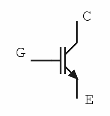
- IGBT is a three-terminal semiconductor device with huge bipolar current-carrying capability. The terminals are emitter, collector and gate.
- This device is designed to make use of the benefits of both BJT and MOSFET devices in the form of monolithic. It combines the best qualities of both to attain the characteristics of an optimal device.
- Two of its terminals namely collector and emitter are associated with a conductance path and the remaining terminal ‘G’ is associated with its control.
- The sum of amplification is achieved by the IGBT is a radio between its input and output signal.
- For a conventional BJT, the amount of gain is almost equal to the ratio to the o/p current to the i/p current that is called a beta.
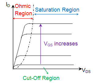
Fig 11. IGBT Symbol
For MOSFET there is no i/p current as the gate terminal is isolated from the main current-carrying channel. Thus, the gain of the field effect transistor equals to the FET’s gain which is equal to the ratio of o/p current change to i/p voltage change.
Then the IGBT can be treated as a power BJT and the base current of this transistor is provided by an MOSFET. The IGBT is mainly used in small-signal amplifier circuits like BJT or MOSFET
When the transistor combines the lower conduction loss of a BJT and MOSFET, then an ideal solid state switch occurs which is perfect for various applications of power electronics.
An IGBT is simply switched “ON” and “OFF” by triggering and disabling its Gate terminal. A constant +ve voltage i/p signal across the ‘G’ and the ‘E’ will retain the device in its “ON” state, while deduction of the i/p signal will cause it to turn “OFF” like BJT or MOSFET.
Structure:
This structure is plain that is the IGBTs silicon cross section is almost equal to that of a vertical power MOSFET except P+ injecting layer.
It shares the same structure of MOS gate & P-wells with N+ source regions. In the following structure, the N+ layer is located at the top is called as the source and the bottom layer is called as a drain or collector.
IGBT takes a parasitic thyristor includes the 4-layer NPN structures. There are some IGBs that are fabricated without the N+ buffer layer called as NPT IGBTS (non punch through).
Some IGBTs are fabricated with the N+ buffer layer called as PT IGBTs (punch through). The performance of the device can considerably increase by the existing buffer layer. The operation of an IGBT is faster when compared to power BJT than power MOSFET.
Circuit Diagram
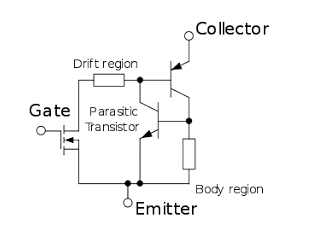
- A simple circuit is drawn using PNP and NPN Transistors, JFET, MOSFET, that is shown in the below figure. The collector terminal of the NPN transistor is connected to the base terminal of the PNP via JFET transistor.
- These transistors signify the parasitic thyristor which creates a regenerative feedback loop. The RB resistor signifies the shorting of the base-emitter terminals of the NPN transistor to ensure that the thyristor doesn’t latch up, that will lead to the IGBT latch-up.
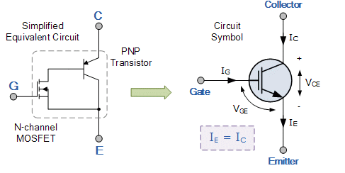
Fig 12. Circuit diagram
The JFET transistor signifies the construction of current between any two adjacent IGBT cells. It allows the MOSFET and supports most of the voltage.
IGBT Characteristics
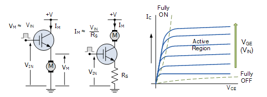
Because IGBT is a voltage-controlled device, it only requires a small voltage on the Gate to maintain conduction through the device.
IGBT is a unidirectional device, meaning it can only switch current in the “forward direction”, that is from Collector to Emitter .
The principal of operation and Gate drive circuits for the insulated gate bipolar transistor are very similar to that of the N-channel power MOSFET. The basic difference is that the resistance offered by the main conducting channel when current flows through the device in its “ON” state is very much smaller in the IGBT. Because of this, the current ratings are much higher when compared with an equivalent power MOSFET.
Advantages
- High voltage capability.
- Low ON-resistance.
- Ease of drive.
- Relatively fast switching speeds and combined with zero gate drive current makes it a good choice for moderate speed.
- High voltage applications such as in pulse-width modulated (PWM), variable speed control, switch-mode power supplies or solar powered DC-AC inverter and frequency converter applications operating in the hundreds of kilohertz range.
IGBTs are used where there is a need for well-controlled, medium-speed switching, and they can be cheaper than comparable silicon MOSFETs. In addition, IGBTs can handle higher voltages than traditional MOSFETs, but that comes with high switching losses when silicon is used. Those losses generate heat, resulting in a need for costly and large thermal management solutions and a limitation on power-conversion system efficiency.
In fact, just the thermal management components required when a silicon IGBT is used will significantly increase both the size and weight of the system, which can be a serious issue for designs involving electric vehicles or aerospace applications. However, for lower switching speeds, IGBTs offer good efficiency and energy savings, which is why for many years they were preferred over comparable MOSFETs.
The excellent thermal conductivity of silicon carbide MOSFETs allows for better thermal conductivity and lower switching losses. The reduced switching losses alone (even at high voltages) mean far less heat generation, thus reducing the thermal management requirements of systems using silicon carbide MOSFETs as opposed to silicon IGBTs.
This, in turn, leads to lower overall costs as well as a far more compact, weight-saving design compared. In addition, silicon carbide MOSFETs are more rugged than silicon IGBTs, making them ideal for harsh environment applications that IGBTs would find challenging, such as onboard chargers for electric vehicles or solar power systems.
Overall, a wise approach would be to consider the use of silicon carbide MOSFETs when deciding what type of component to use for a design. Taking into consideration the high switching speeds, reduced switching losses, higher efficiency, and ruggedness of silicon carbide MOSFETs compared to their silicon IGBT counterparts, it is easy to see why more and more engineers are opting for silicon carbide power components. Silicon carbide offers more reliable, sustainable designs with better overall efficiency, a smaller footprint, and less weight.
SCR ratings
Latching Current (IL): Latching current IL is the minimum anode current required to maintain thyristor in ON state immediately after thyristor has been Turn ON and the gate signal has been removed
Holding Current (IH): Minimum anode current below which device stop conducting and return to its off state usually this value is very small in mA.
Forward Breakdown Voltage (VBO): If anode to cathode voltage VAK is increase to sufficient large value, the reverse bias junction J2 breaks this is known as Avalanche Breakdown and corresponding voltage is called as forward breakdown voltage VBO.
Reverse Breakdown Voltage (VBR): If reverse voltage is increased During reverse blocking if Ig = 0 then only reverse saturation current (Is) flows until the reverse voltage reaches reverse break down voltage (VBR). At this point current starts rising sharply. Large reverse voltage and current generates excessive heat and destroys the device.
Dv/dt: dv/dt rating of thyristor indicates maximum rate of rise of anode voltage that will not trigger the device without any gate signal.
Di/dt: di/dt rating of thyristor indicates maximum rate of rise of anode to cathode current.
Surge Current: It specifies the maximum allowable non repetitive current the device can withstand. The device is assumed to be operating under rated blocking voltage, forward current and junction temperature before the surge current occurs. Following the surge the device should be disconnected from the circuit and allowed to cool down.
Rated Current
It is the current in which all appliances maximum limiting current.
Gate characteristics
Gate characteristic of thyristor or SCR gives us a brief idea to operate it within a safe region of applied gate voltage and current. At the time of manufacturing each SCR or thyristor is specified with the maximum gate voltage limit (Vg-max), gate current limit (Ig-max) and maximum average gate power dissipation limit (Pgav).
These limits should not be exceeded to protect the SCR from damage and there is also a specified minimum voltage (Vg-min) and minimum current (Ig-min) for proper operation of a thyristor.
A gate non triggering voltage (Vng) is also mentioned at the time of manufacturing of the device.
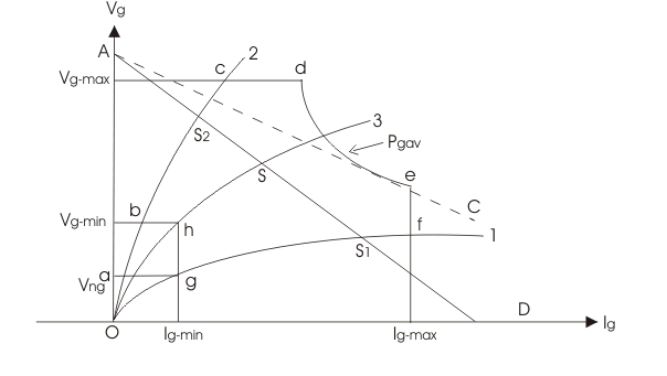
Curve 1 represents the lowest voltage values that must be applied to turn on the SCR and
Curve 2 represents the highest values of the voltage that can safely applied.
So from the figure we can see the safety operated area of SCR is bcdefghb.
Now, from the triggering circuit, we get,
Es = Vg + Ig Rs -----------------(1)
Where,
Es = gate source voltage
Vg = gate cathode voltage
Ig = gate current
Rs = gate source resistance
A load line of gate source voltage is drawn as AD where OA = Es and OD = Es/Rs which is trigger circuit short circuit current.
Now, the VI characteristic of gate circuit is given by curve 3. The intersection point of load line (AD) and curve 3 is called as operating point S.
It is evident that S must lie between S1 and S2 on the load line. For decreasing the turn ON time and to avoid unwanted turn ON of the device, operating point should be as close to Pgav as possible.
Slop of AD = source resistance Rs. Minimum amount of Rs can be determined by drawing a tangent to the Pgav carve from the point A.
Gate drive requirements
- A MOSFET has a significant gate capacitance that must be charged or discharged whenever the device is switched on or off. The drive circuit must supply high peak current to quickly turn on the MOSFET. Conversely, the driver is required to sink a similar amount of current to ground to turn off the device. This sequence repeats at the operating frequency of the power transistor.
- Increasing the switching frequency imposes additional requirements on the driver circuitry, including operation at voltages of 5 V or lower, low propagation delay, tight matching between channels, and minimum parasitic inductance.
- A complex power design often relies on a digital device such as a microcontroller to control the power delivery, calculate pulse-width-modulation (PWM) frequency, handle diagnostics, and generate the turn-on or turn-off signal.
Gate drive circuits for MOSFET and IGBT
- A gate drive circuit is an integrated circuit that accepts a low power input from a controller IC and produces the appropriate voltage and current for a power semiconductor switch.
- The figure shows the printed circuit board of two gate drive circuits which are driving the two MOSFETS of a three-phase inverter leg.
- A gate driver sometimes includes also the protection circuit of the semiconductor switch.
- Gate drivers may be implemented as dedicated ICs, discrete transistors, or transformers.
- They can also be integrated within a controller IC. The MOSFET switching speed depends on the gate current that charges the parasitic capacitances of the semiconductor device.
- Therefore, the engineer has the capability to adjust the switching times (i.e., toff and ton) of a MOSFET through the design of the driving circuits.
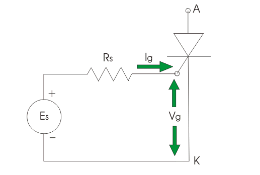
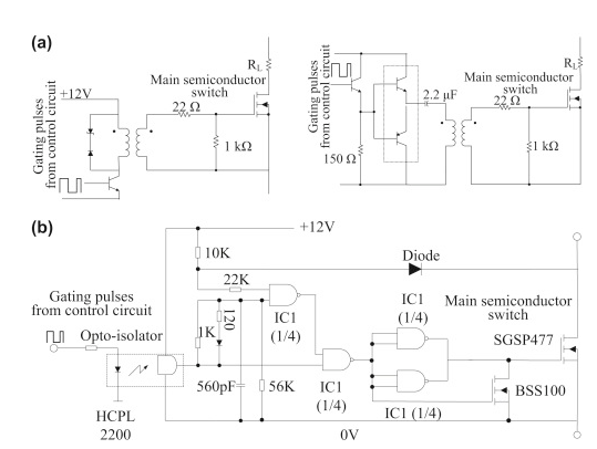
Fig 13(a) and (b) show some examples of gate drive circuits that can be used to drive power MOSFETs.
The gate drive circuits of Fig. (a) are applied directly to the MOSFET without any ohmic isolation.
However, there are applications where the gate drive circuit must exhibit ohmic or galvanic isolation in order to prevent short-circuit problems within a power converter The figure shows three different gate drive circuits that provide ohmic isolation between the control circuit of a converter and the power semiconductor devices.
As can be seen from the figure the ohmic isolation is achieved using an opto-isolator or a transformer. The opto-isolator is used in applications where the duty cycle of the gating pulses is over 50%.
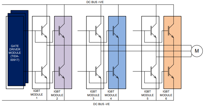
- Insulated gate bipolar transistors (IGBTs) are considerably used in three-phase inverters that have numerous applications like variable-frequency drives that control the speed of AC motors, uninterruptible power supplies (UPS), solar inverters, and other similar inverter applications.
- IGBTs have the advantages of high-input impedance as the gate is insulated, has a rapid response ability, good thermal stability, simple driving circuit, good ability to withstand high voltage, snubber-less operation, and controllability of switching behavior providing reliable short-circuit protection.
- The IGBT is a voltage controlled device, which gives it the ability to turn on and off very quickly. Paralleling IGBT modules becomes necessary when the output current requirement cannot be provided by a single IGBT module.
- A single module of an IGBT is capable of handling currents up to 600 A in the dual configuration. Higher currents in the range of kilo amperes are required in case of high power rated equipments.
- Higher currents can be obtained either by paralleling inverters or by paralleling the IGBT modules inside the inverter as shown in Figure 1. An advantage of paralleling includes distributing heat sources so that higher levels of power loss can be dissipated.
Opto-isolator driving circuit for SCR
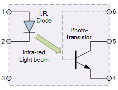
An optocoupler or opto-isolator consists of a light emitter, the LED and a light sensitive receiver which can be a single photo-diode, photo-transistor, photo-resistor, photo-SCR, or a photo-TRIAC with the basic operation of an optocoupler being very simple to understand.
- The photo-transistor device is shown in the figure. The current from the source signal passes through the input LED which emits an infra-red light whose intensity is proportional to the electrical signal.
- This emitted light falls upon the base of the photo-transistor, causing it to switch-ON and conduct in a similar way to a normal bipolar transistor.
- The base connection of the photo-transistor can be left open (unconnected) for maximum sensitivity to the LEDs infra-red light energy or connected to ground via a suitable external high value resistor to control the switching sensitivity making it more stable and resistant to false triggering by external electrical noise or voltage transients.
- When the current flowing through the LED is interrupted, the infra-red emitted light is cut-off, causing the photo-transistor to cease conducting.
- The photo-transistor can be used to switch current in the output circuit. The spectral response of the LED and the photo-sensitive device are closely matched being separated by a transparent medium such as glass, plastic or air. Since there is no direct electrical connection between the input and output of an optocoupler, electrical isolation up to 10kV is achieved
Series and Parallel operation of SCR
Series Operation
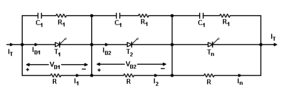
In series configuration it increases the voltage ratings while the current ratings remain the same. Thyristors of same type do not have same I-V and off state characteristics.
So the voltage drop across the thyristors would be unequal. To solve this issue following parameters are set by default.
- Resistors are connected across each thyristor to avoid the unequal voltage sharing.
- The values of the resistors must be selected, so the equivalent resistance of thyristor and resistor would be same.
- To get best results we may use this formula to find out the value of resistor.
R = nvbm – vs /(n-1) 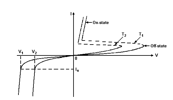 b
b
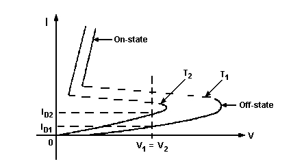
Now, the off state currents would be as shown in the figure:
Parallel operation of thyristors
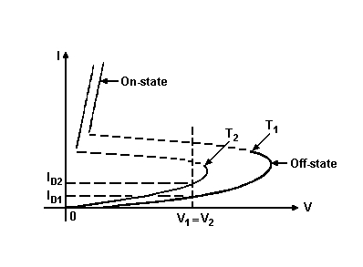
If the load current increases from the current rating of a single thyristor, then the parallel configuration is used. The same problem arises here as well. Current is not shared equally among the thyristors as the V-I characteristics are not similar.
Thermal Runaway
Power is dissipated by the thyristors which carry high current. This power dissipation causes the junction temperature to increases, decreasing the internal resistance. This can damage the thyristor which is termed as thermal runaway. Thermal runaway can be avoided by following these steps:
- There should be a common heat sink, making sure that the thyristors operate at similar temperature.
- Current sharing should be equal. For this resistors or inductors may be used in series with the thyristors.
Static current sharing
Resistors are used in case of static current sharing. When resistances are used in series, the losses may become high.

Dynamic current sharing
For dynamic current sharing, inductors are also used in addition to the resistors. In case of inductors if current through the thyristor T1 increases, an opposite polarity voltage would be induced in the series coil of thyristor T2. The current flow is increased through the thyristor, serving the purpose.
Applications of power devices as a switch
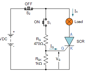
When connected to a direct current DC supply, the thyristor can be used as a DC switch to control larger DC currents and loads.
When using the Thyristor as a switch it behaves like an electronic latch because once activated it remains in the “ON” state until manually reset.
Consider the DC thyristor circuit below
Solved Examples
Q1) An SCR has a breakover voltage of 400 V, a trigger current of 10 mA and holding current of 10 mA. What do you infer from it? What will happen if gate current is made 15 mA?
A1)
(i) Breakover voltage of 400 V. It means that if gate is open and the supply voltage is
400 V, then SCR will start conducting heavily. However, as long as the supply voltage is less than 400 V, the SCR stays open i.e. it does not conduct.
(ii) Trigger current of 10 mA. It means that if the supply voltage is less than breakover voltage (i.e. 400 V) and a minimum gate current of 10 mA is passed, the SCR will close i.e. starts conducting heavily. The SCR will not conduct if the gate current is less than 10 mA. It may be emphasised that triggering is the normal way to close an SCR as the supply voltage is normally much less than the breakover voltage.
(iii) Holding current of 10 mA. When the SCR is conducting, it will not open (i.e. stop conducting) even if triggering current is removed. However, if supply voltage is reduced, the anode current also decreases. When the anode current drops to 10 mA, the holding current, the SCR is turned off.
(iv) If gate current is increased to 15 mA, the SCR will be turned on lower supply voltage.
Q2) An SCR in a circuit is subjected to a 50 A surge that lasts for 12 ms. Determine whether or not this surge will destroy the device. Given that circuit fusing rating is 90 A2s.
A2) Circuit fusing rating = I2t = (50)2 × (12 × 10−3) = 30 A2s.
Since this value is well below the maximum rating of 90 A2 s, the device will not be destroyed.
Q3) An SCR has a circuit fusing rating of 50 A2 s. The device is being used in a circuit where it could be subjected to a 100 A surge. Determine the maximum allowable duration of such a surge.
A3) tmax = I2t (rating)/I2s = 50/(100)2 = 5x10-3 = 5ms
Q4) A 220Ω resistor is connected in series with the gate of an SCR. The gate current required to fire the SCR is 7mA. What is the input voltage (Vin) required to fire the SCR?
A4) The input voltage must overcome the junction voltage between the gate and cathode (0.7V) and also cause 7mA to flow through the 220Ω resistor. According to Kirchhoff’s voltage law, Vin is given by
Vin = VGK + IGR = 0.7V + (7mA) (220Ω) = 2.24V
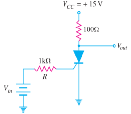
Q5) The SCR of Figure has gate trigger voltage VT = 0.7V, gate trigger current IT = 7 mA and holding current IH = 6 mA. (i) What is the output voltage when the SCR is off? (ii) What is the input voltage that triggers the SCR? (iii) If VCC is decreased until the SCR opens, what is the value of VCC?
A5)
(i) When the SCR is off (i.e. it is not conducting), there is no current through the 100Ω resistor.
∴ Vout = Supply voltage VCC = 15V
(ii) The input voltage Vin must overcome VT (=0.7V) and also cause 7 mA to flow through 1 kΩ resistor.
∴ Vin = VT + IT R = 0.7 + (7 mA) (1 kΩ) = 7.7V
(iii) In order to open the SCR, the VCC must be reduced so that anode current is equal to IH.
∴ IH = VCC - VT /100Ω
VCC = (100Ω) (IH) + VT = (100Ω) (6 mA) + 0.7 = 1.3V
Q6) In Figure, the SCR has a trigger voltage of 0.7 V. Calculate the supply voltage that turns on the crowbar. Ignore Zener diode resistance.
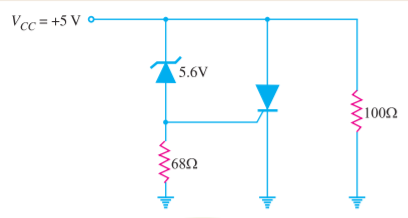
A6) The breakdown voltage of the Zener is 5.6V. To turn on the SCR, the voltage across 68Ω has to be equal to VT (= 0.7V).
∴ VCC = VZ + VT = 5.6 + 0.7 = 6.3V
When the supply voltage becomes 6.3 V, the Zener breaks down and starts conducting. The voltage VT (= 0.7V) across 68Ω forces the SCR into conduction. When the SCR conducts, the supply voltage is shorted by the SCR and the fuse in the supply voltage burns out. Thus, the load (100Ω) is protected from overvoltage.
Q7) The Zener diode of Figure has a tolerance of ± 10% and the trigger voltage can be as high as 1.5V. What is the maximum supply voltage where crowbarring takes place?
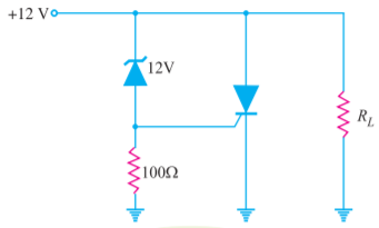
A7) The breakdown voltage of the Zener diode is 12V and it has a tolerance of ± 10%. It means that breakdown voltage of Zener can vary from 10.8V to 13.2V. Since the trigger voltage of SCR has a maximum value of 1.5 V
∴ Maximum value of supply voltage for crowbarring = 13.2V + 1.5V = 14.7V
Q8) The circuit of Figure is in a dark room. When a bright light is turned on, the LASCR fires. What is the approximate output voltage? If the bright light is turned off, what is the output voltage?
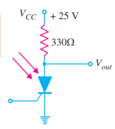
A8) Figure shows a light-activated SCR, also known as a photo-SCR. When light falls on the device, it starts conducting and the output voltage is ideally, Vout = 0V However, if we take into account anode-cathode drop, Vout = 0.7V. When light is turned off, the LASCR stops conducting and the output voltage is equal to the supply voltage VCC
Vout = VCC = + 25V
Q9) Give a simple method for testing an SCR?
A9)
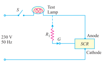
Figure shows a simple circuit for testing an SCR. The test lamp serves two purposes. First, it is a visual indicator of current conduction. Secondly, it limits current through the SCR.
(i) When switch S is closed, the lamp should not light for the SCR to be good. It is because voltage is applied only between anode and cathode but there is no trigger voltage. If the lamp lights, the SCR is shorted.
(ii) Now touch R1 momentarily between gate and anode terminals. For the SCR to be good, the lamp should light and continue to light. If it does not, the SCR is open. Note that the lamp will be on at half brilliance because the SCR conducts only every other half cycle.
Q10) Determine the input voltage necessary to cause the breakdown in SCR for 200 Ω resistance connected in series if the required gate current for firing is 6 mA.
A10) In accordance to the given data and the reference diagram, it is mandatory to estimate the value of input voltage in such a manner that it should overcome the barrier voltage of 0.7 V.
Secondly, it should allow the current of 6 mA to flow through the resistor of about 200 Ω.
Hence, from the figure, the value of input voltage can be estimated as,
Input Voltage = Gate to Cathode Voltage + (Gate Current x Resistance)
Thus, Vin = VGC + IG R
= 0.7 +( 6 x 10-3 x 200 )
= 0.7 + (1200 x 10-3 )
= 1.9 V
References:
- Power Electronics by Muhammad H Rashid
- Power Electronics by Evolution, Technology and applications by A.K.Bose
- Ned Mohan, T. Undeland & W. Robbins, “Power Electronics Converters Applications and Design, John Willey & sons, Singapore, 2nd Edition Oxford University Press, New Delhi, 2005.
- Muhammad H. Rashid, “Power Electronics Handbook”, Academic Press, 2nd Edition, 2001