Unit - 2
AC to DC Power Converters
The turn off process of SCR is termed as commutation. Commutation means the transfer of currents from one path to another. The commutation circuit performs the task of reducing the current to zero in order to turn OFF the SCR.
In order to turn OFF the conducting SCR, the following conditions must be satisfied.
- The anode or forward current of SCR must be reduced to zero or below the level of holding current.
- A sufficient reverse voltage must be applied across the SCR to regain its forward blocking state.
The SCR is turned OFF by reducing forward current to zero. Then there exists excess charge carriers in different layers. In order to regain the forward blocking state of an SCR, these excess carriers must be recombined. Therefore, this recombination process can accelerated by applying a reverse voltage across the SCR.
SCR Turn OFF Methods
The reverse voltage, which causes the SCR to commutate is called commutation voltage. The commutation methods are classified into two major types depending on the location of the commutation voltage.
They are
- Forced commutation
- Natural commutation
Natural Commutation
- In natural commutation, the source of commutation voltage is the supply source itself.
- If the SCR is connected to an AC supply, at the end of every positive half cycle the anode current goes through the natural current zero and also immediately a reverse voltage is applied across the SCR.These are the conditions to turn OFF the SCR.
- This method of commutation is also called as source commutation, or line commutation, or class F commutation.
- This commutation is possible with line commutated inverters, controlled rectifiers, cyclo converters and AC voltage regulators because the supply is the AC source in all these converters.
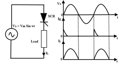
Forced Commutation
- In case of DC circuits, there is no natural current zero to turn OFF the SCR. In such circuits, forward current must be forced to zero with an external circuit to commutate the SCR hence termed as forced commutation.
- This commutating circuit consists of components like inductors and capacitors called as commutating components. These commutating components cause to apply a reverse voltage across the SCR that immediately bring the current in the SCR to zero.
- Based on the manner in which the zero current is achieved and the arrangement of the commutating components, forced commutation is classified into different types such as class A, B, C, D, and E. This commutation is mainly used in chopper and inverter circuits.
Single Phase Semi converters
- In phase control, thyristors are used as switches to connect the load circuit to the input ac supply, for a part of every input cycle.
- That is the ac supply voltage is chopped using Thyristors during a part of each input cycle.
- The thyristor switch is turned on for a part of every half cycle, so that input supply voltage appears across the load and then turned off during the remaining part of input half cycle to disconnect the ac supply from the load.
- Single phase ac controllers operate with single phase ac supply voltage of230V RMS at 50Hz
Single Phase Semi converters for R load
A single phase half wave thyristor converter which is used for ac-dc power conversion is shown in the above figure. The input ac supply is obtained from a main supply transformer to provide the desired ac supply voltage to the thyristor converter depending on the output dc voltage required. P v represents the primary input ac supply voltage. S v represents the secondary ac supply voltage which is the output of the transformer secondary.
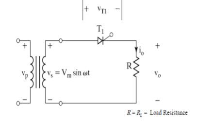
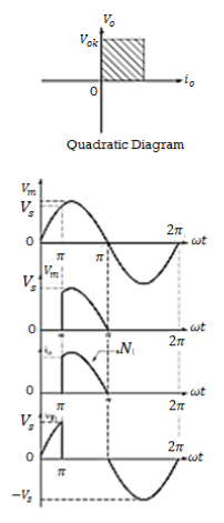
During the positive half cycle of input supply when the upper end of the transformer secondary is at a positive potential with respect to the lower end, the thyristor anode is positive with respect to its cathode and the thyristor is in a forward biased state. The thyristor is triggered at a delay angle of ωt =α, by applying a suitable gate trigger pulse to the gate lead of thyristor. When the thyristor is triggered at a delay angle of ωt =α, the thyristor conducts and assuming an ideal thyristor, the thyristor behaves as a closed switch and the input supply voltage appears across the load when the thyristor conducts from ωt =αto πradians. Output voltage 𝑉𝑂 = 𝑉𝑆 when the thyristor conducts from ωt =αto π. For a purely resistive load, the load current O i (output current) that flows when the thyristor T1 is on, is given by the expression
𝑖𝑜 = 𝑉𝑂/, 𝑓𝑜𝑟 𝛼 ≤ 𝜔𝑡 ≤ π.
The output load current waveform is similar to the output load voltage waveform during the thyristor conduction time from αto π. The output current and the output voltage waveform are in phase for a resistive load. The load current increases as the input supply voltage increases and the maximum load current flows at = 𝜋 2 , when the input supply voltage is at its maximum value. The maximum value (peak value) of the load current is calculated as
𝑖𝑜 𝑚𝑎𝑥 = 𝐼𝑚 = 𝑉𝑚 𝑅𝐿
Note that when the thyristor conducts (𝑇1 is on) during ωt =αto π, the thyristor current 𝑖𝑇1 , the load current 𝑖𝑂through 𝑅𝐿and the source current 𝑖𝑠 flowing through the transformer secondary winding are all one and the same. Hence we can write 𝑖𝑠 = 𝑖𝑇1 = 𝑖𝑜 = 𝑉𝑂/ 𝑅 = 𝑉𝑚 sin 𝜔𝑡 𝑅 ; 𝑓𝑜𝑟 𝛼 ≤ 𝜔𝑡 ≤ 𝜋 𝐼𝑚 is the maximum (peak) value of the load current that flows through the transformer secondary winding, through 𝑇1 and through the load resistor 𝑅𝐿at the instant 𝜔𝑡 = 𝜋 2 , when the input supply voltage reaches its maximum value.
When the input supply voltage decreases the load current decreases. When the supply voltage falls to zero at ωt =π, the thyristor and the load current also falls to zero at ωt =π. Thus the thyristor naturally turns off when the current flowing through it falls to zero at ωt =π.
During the negative half cycle of input supply when the supply voltage reverses and becomes negative during ωt =πto 2πradians, the anode of thyristor is at a negative potential with respect to its cathode and as a result the thyristor is reverse biased and hence it remains cutoff (in the reverse blocking mode).
The thyristor cannot conduct during its reverse biased state between ωt =πto 2π. An ideal thyristor under reverse biased condition behaves as an open switch and hence the load current and load voltage are zero during ωt =πto 2π. The maximum or peak reverse voltage that appears across the thyristor anode and cathode terminals is . The trigger angle α(delay angle or the phase angle α) is measured from the beginning of each positive half cycle to the time instant when the gate trigger pulse is applied. The thyristor conduction angle is from αto π, hence the conduction angle δ= (π−α) . The maximum conduction angle is π radians (1800 ) when the trigger angle α= 0 .
Single Phase Semi-Converter with R-L Load
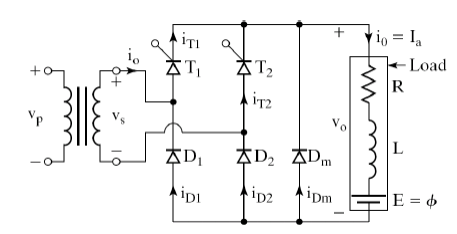
- Consider thyristors T1 and T2 and D1 and D2 as shown in the figure . The two thyristors are controlled power switches, which are turned on one after the other by applying suitable gating signals (gate trigger pulses).
- The two diodes are uncontrolled power switches which turn-on and conduct one after the other as and when they are forward biased.
- The circuit diagram of a single -phase semi-converter half -controlled bridge converter is shown in the above figure with highly inductive load and a dc source in the load circuit.
- When the load inductance is large the load current flows continuously and we can consider the continuous load current operation assuming constant load current.
- The ac supply to the semi-converter is fed through a mains supply transformer having suitable turn’s ratio. The transformer is suitably designed to supply the required ac supply voltage.
- During the positive half cycle of input ac supply voltage, when the transformer secondary output line ‘A’ is positive with respect to the line ‘B’ the thyristor T1 and the diode D1are both forward biased. The thyristor T1is triggered at ωt =α; (0 ≤α≤π) by applying an appropriate gate trigger signal to the gate of T1.
- The current in the circuit flows through the secondary line ‘A’, through T1, through the load in the downward direction, through diode D1back to the secondary line ‘B’.
- T1 and D1conduct together from ωt =αto π and the load is connected to the input ac supply.
- The output load voltage follows the input supply voltage that is the secondary output voltage of the transformer during the period ωt =α to π.
- At ωt =π, the input supply voltage decreases to zero and becomes negative during the period ωt =π to (π+α) . The freewheeling diode Dm across the load becomes forward biased and conducts during the period ωt =π to (π+α) .
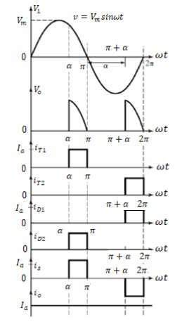
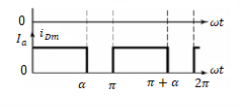
- The load current is transferred from T1and D1 to the FWD Dm. T1and D1are turned off. The load current continues to flow through the FWD Dm. The load current free wheels that is flows continuously through the FWD during the free -wheeling time period π to (π+α).
- During the negative half cycle of input supply voltage the secondary line ‘A’ becomes negative with respect to line ‘B’. The thyristor T2and the diode D2are both forward biased. 2 T is triggered at ωt = (π+α) , during the negative half cycle. The FWD is reverse biased and turns-off as soon as 2 T is triggered. The load current continues to flow through 2 T and 2 D during the period ωt = (π+α) to 2π.
Derive an expression for the average or DC output voltage of a single phase semiconductor.
Vdc = 2/2π  d(wt)
d(wt)
= 2Vm/2π[-coswt] α π
= 2Vm /2 π [-cosπ + cosα]
= Vm /π [ 1+cosα]
Vdc = Vm/π[ 1 + cos α]
Vdc can be varied from 2𝑉𝑚 𝜋 to 0 by varying αfrom 0 to π. The maximum average output voltage is
Vdc(max) = 2Vm/π
Normalizing the average output voltage with respect to its maximum value
𝑉𝑑𝑐𝑛 = 𝑉𝑛 = 𝑉𝑑𝑐
𝑉𝑑𝑚 = 0.5 (1 + cos 𝛼)
The output control characteristic can be plotted by using the expression for Vdc.
To Derive An Expression for the RMS Output Voltage of a Single Phase Semi-Converter
The rms output voltage is found from
Vo(rms) = [2/2π  2 sin 2 wt d(wt)] ½
Vo(rms) = [Vm 2/π  sin 2 wt d(wt)] ½
Vo(rms) = [Vm 2/2π  )] ½
)] ½
Vo(rms) = [Vm 2/
 (π-α + sin 2α/2)] ½
Problems:
Q1) The single-phase half wave rectifier has a purely resistive load of R and the delay angle is α=π/2, determine: 𝑉𝑑𝑐, 𝐼𝑑𝑐, 𝑉𝑟𝑚𝑠, 𝐼𝑟𝑚𝑠.
A1)


Q2) Design a circuit to produce an average voltage of 40V across a 100Ω load resistor from a 120Vrms 60-Hz ac source. Determine the power absorbed by the resistance and the power factor.
A2)


Q3) For the circuit of controlled half-wave rectifier with RL Load, the source is 120Vrms at 60 Hz, R=20Ω, L=0.04H, and the delay angle is 45o. Determine (a) an expression for i(𝜔t), (b) the rms current, (c) the power absorbed by the load, and (d) the power factor.
A3)
(a) 


(b)

(c)

(d)

Q4) The full-wave controlled bridge rectifier has an ac input of 120Vrms at 60 Hz and a 20Ω load resistor. The delay angle is 40o. Determine the average current in the load, the power absorbed by the load, and the source voltamperes.
A4) 


The rms current in the source is also 5.80 A and the apparent power of the source is


Q5) A controlled full-wave bridge rectifier has a source of 120Vrms at 60Hz, R=10Ω, L=20mH, and α=60o. Determine (a) an expression for load current, (b) the average load current, and (c) the power absorbed by the load.
A5)


(a)

Solving  numerically for , =3.78 rad (216°). Since π+=4.19>
The current is discontinuous and the above expression for current is valid.
(b) 
(c) 

(d) 
Q6) A single phase 230V, 1kW heater is connected across 1-phase 230V, 50Hz supply through an SCR. For firing angle delay of 450 and 900, calculate the power absorbed in the heater element?
A6)
Heater resistance 
The value of rms voltage for = is
is

Power absorbed by heater element for = is
is

For = , rms voltage is

Power absorbed for  is
is

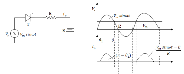
Q7) A dc battery is charged through a resistor R as shown in fig. (a) Derive an expression for the average value of charging current in terms of  On the assumption that SCR is fired continuously.
(a) For an ac source voltage of 230 V, 50 Hz, find the value of average charging current for R=8 and #=150 V
(b) Find the power supplied to battery and that dissipated in the resistor.
(c) Find the supply pf.
A7)
For the circuit of the voltage equation is


It is seen from fig. That SCR is turned on when  and is turned off when
  where
where  .
.
The battery charging requires only the average current  given by


(a) Here 

(b) Power supplied to battery 
For finding the powr dissipated in R, rms value of charging current must by obtained

Power dissipated in resistor 
(c) suuply pf
Q8) A 230 V, 50 Hz one-pulse SCR controlled converter is triggered at a firing angle f of 40° and the load current extinguishes at an angle of 210°. Find the circuit turn off time, average output voltage and the average load current for
(a) 
(b) 
A8)
(a) circuit turn off time 

Average output voltage

Average load current 
(b) Fig shows that circuit turn-off time is again 8.333 m-sec average load current

Average load voltage, 
Q9) SCRs with forward voltage rating of 100 V and average on-state current rating of 40 A are used in single-phase mid-point converter and single-phase bridge converter. Find the power that these two converters can handle. Use a factor of safety of 2.5
A9)
Maximum voltage across SCR in single-phase mid-point converter is 2 
Therefore this converter can be designed for a maximum voltage of 
Maximum average power that mid-point converter can handle

SCR in a single-phase bridge converter is subjected to a maximum voltage of 
Therefore maximum voltage for which this converter can be designed is

Maximum average powr rating of bridge converter

Q10) A single phase full converter bridge is connected to RLE load. The source voltage is 230 V, 50 Hz. The average load current of 10 A is continuous over the working range. For R=0.4× and L=2m H compute
(a) firing angle delay for E=120 V
(b) firing angle delay for E=-120V
(c) In case output current is assumed constant find the input pf for both parts (a) and (b)
A10)
(a) For E=120 V the full converter is operating as a controlled rectifier


=53.208
For =53.21° power flows from ac source to dc load
(b) For E=-120 V, the full converter is operating as a line commutated inverter.

For a=124.1° the power flows from dc source to ac load
(c) For constant load current, rms value of load current  is
is

For 
For 
Q11) A single phase full wave ac voltage controller supplies an RL load. The input supply voltage is 20V, RMS at 50 Hz. The load has L=10mH and R=10Ω. The delay angle of thyristors T1 and T2 are equal where  . Determine
- Conduction angle of the thyristors T1.
- RMS output voltage
- The input power factor.
Given:
Vs= 23 0V f= 50Hz L = 10mH R=10Ω  60 o
60 o
 1=
1=
 radians.
Vm =  Vs =
Vs =  x 230 = 352.2691193V
Z = Load Impedance = [R2 + (wL)2]1/2 = [10 2 + (2π x0x10x10-3)2 ]1/2 = 10.4818Ω.
Im= Vm/Z =  x 230/10.4818 = 31.03 A
Load Impedance Angle:
 = tan -1 (wL/R)
 = 17.44059
Trigger angle  . Hence the type of operation will be discontinuous and load current operation we get is
β<(π + α)
β < 240
Extinction angle
β is calculated by using the equation
Sin(β - ) = sin (α - ) e –R/wL(β – α).
In the exponential term the value of α and β should be in radians. Hence
Sin(β – ) = sin(α - ) e –R/wL(βrad – α rad) ; α rad = (π/3)
(α - ) = (60 – 17.44059) = 42.5594 0
Sin(β – 17.44) = sin(42.5594) e -10/π(β – α) = 0.67635 e-3.183(β-α)
β rad = β o x π / 180 assuming β o = 190
β rad = 3.3161
LHS sin(190-17.44) = sin(172.5594) = 0.129
RHS 0.67635 e-3.183(β-α) = 4.94 x 10 -4
Assuming β = 197.42
β rad = β o x π / 180 = 3.446
L.H.S = sin(β - ) = sin( 197.42 – 17.44) = 3 .4906 x 10 -4.
R.H.S = 0.67635 e -3.183(3.4456-π/3) = 3.27 x 10 -4
Conduction angle  (β – α) = 197.42-60 = 137.42 o
RMS output voltage
Vo(rms) = Vs [(1/π (β –  sin2
sin2 - sin 2β/2 ] ½
Vo(rms) = 230 [(1/π (3.4456 – π/3) + sin2(60 o )/2 – sin2(197.42 0 )/2 ]1/2
Vo(rms) = 207.045 V.
Q12) A single phase half wave ac regulator using one SCR in anti-parallel with a diode feeds 1kW 230V heater. Find the load power for a firing angle of 45 0 .?
A12)
 0 = π/4 Vs = 230V Po = 1KW
Po = Vo Io = Vo x Vo/R = Vo 2 /R
Resistance of the heater
R = Vo2/ P0 = (230) 2/ 1000= 52.9 Ω
RMS value of output voltage
Vo = Vs [1/2π (2π – α) + sin2α/2] ½
Vo = 230[1/2π(2π – π/4) + sin 90/2] ½ = 224.7517 V
Single Phase Full Converter (Fully Controlled Bridge Converter)
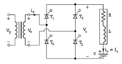
The circuit diagram of a single phase fully controlled bridge converter is shown in the figure with a highly inductive load and a dc source in the load circuit so that the load current is continuous and ripple free that is constant load current operation.
The fully controlled bridge converter consists of four thyristors T1, T2,T3 and T4 connected in the form of full wave bridge configuration as shown in the figure. Each thyristor is controlled and turned on by its gating signal and naturally turns off when a reverse voltage appears across it.
During the positive half cycle when the upper line of the transformer secondary winding is at a positive potential with respect to the lower end the thyristors T1and T2are forward biased during the time interval ωt = 0 to π.
- The thyristors T1and T2are triggered simultaneously ωt =α; (0 ≤α≤π) , the load is connected to the input supply through the conducting thyristors T1and T2.
- The output voltage across the load follows the input supply voltage and hence output voltage 𝑉𝑂 = 𝑉𝑚 sin 𝜔𝑡. Due to the inductive load T1 and T2will continue to conduct beyond ωt =π, even though the input voltage becomes negative.
- T1 and T2 conduct together during the time period α to (π+α) , for a time duration of π radians meaning the conduction angle of each thyristor = 1800.
- During the negative half cycle of input supply voltage for ωt =π to 2π the thyristors T3and T4 are forward biased. T3 and T4are triggered at ωt = (π+α).
- As soon as the thyristors 3 T and 4 T are triggered a reverse voltage appears across the thyristors T1and T2and they naturally turn-off and the load current is transferred from T1and T2 to the thyristors T3and T4.
- The output voltage across the load follows the supply voltage and 𝑉𝑂 = −𝑉𝑚 sin 𝜔𝑡 during the time period ωt = (π+α) to (2π+α).
- In the next positive half cycle when T1and T2 are triggered, T3and T4are reverse biased and they turn-off.
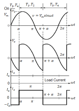
- During the time period ωt =α to π, the input supply voltage VS and the input supply current is are both positive and the power flows from the supply to the load.
- The converter operates in the rectification mode during ωt =αto π. During the time period ωt =π to (π+α), the input supply voltage vs is negative and the input supply current is positive and there will be reverse power flow from the load circuit to the input supply.
- The converter operates in the inversion mode during the time period ωt =π to (π+α) and the load energy is fed back to the input source.
- Depending on the value of trigger angle α, the average output voltage may be either positive or negative and two- quadrant operation is possible.
To Derive an Expression for the Average (DC) Output voltage.
The average (dc) output voltage can be determined by using the expression
Vo(dc) = Vdc = 1/2π [  ----------------------------(1)
The output voltage waveform consists of two output pulses during the input supply time period between 0 & 2π radians . In the continuous load current operation of a single phase full converter assuming constant load current each thyristor conduct for π radians (1800 ) after it is triggered.
When thyristors T1and T2are triggered at ωt =α1 T and 2 T conduct from α to (π+α) and the output voltage follows the input supply voltage.
Therefore output voltage 𝑉𝑂 = 𝑉𝑚 sin 𝜔𝑡 for ωt =α to (π+α).
Hence, the average or dc output voltage can be calculated as
V0(dc) = Vdc = 2/2π  ------------------------(1)
V0(dc) = Vdc = 1/π  ----------------------------(2)
V0(dc) = Vdc = Vm/π  ---------------------------------------(3)
V0(dc) = Vdc = Vm/π [-coswt] α π + α ------------------------------------------(4)
V0(dc) = Vdc =2 Vm/π cos α -----------------------------------------(5)
The dc output voltage Vdc can be varied from a maximum value of 2𝑉𝑚 𝜋 for 𝛼 = 0 𝑎 𝑚𝑖𝑛𝑖𝑚𝑢𝑚 𝑣𝑎𝑙𝑢𝑒 𝑜𝑓 −2𝑉𝑚/ 𝜋 𝑓𝑜𝑟 𝛼 = 𝜋 𝑟𝑎𝑑𝑖𝑎𝑛𝑠 .The maximum average dc output voltage is calculated for a trigger angle α= 0 0 and is obtained as
Vdc(max) = Vdc = 2Vm /π x cos0 = 2Vm/π.
The normalized average output voltage is given by
Vn = V0(dc)/Vdc(max) = 2 Vm/π cos α / 2 Vm/π
Vn = cos α.
Performance Parameters.
Transformer Utilization Factor
TUF = Po(dc) / Vs x Is
Where:
Vs = rms value of transformer secondary output voltage (RMS supply voltage at the secondary)
Is = RMS value of transformer secondary current.
Harmonic Factor (HF) or Total Harmonic Distortion Factor (THD):
The harmonic factor is a measure of the distortion in the output waveform and is also referred to as the total harmonic distortion (THD).
Where
𝐼𝑆 = 𝑅𝑀𝑆 𝑣𝑎𝑙𝑢𝑒 𝑜𝑓 𝑖𝑛𝑝𝑢𝑡 𝑠𝑢𝑝𝑝𝑙𝑦 𝑐𝑢𝑟𝑟𝑒𝑛𝑡
𝐼𝑆1 = RMS value of fundamental component of the input supply current.
Input Power Factor (PF)
𝑃𝐹 = 𝑉𝑆 𝐼𝑆1 / 𝑉𝑆 𝐼𝑆 cos ∅ = 𝐼𝑆1/ 𝐼𝑆 cos ∅
The Crest Factor (CF) 𝐶𝐹 = 𝐼𝑆 𝑝𝑒𝑎𝑘 𝐼𝑆 = Peak input supply current RMS input supply current.
Single phase fully controlled converter with source inductance
Figure below shows a single phase fully controlled converter with source inductance. For simplicity it has been assumed that the converter operates in the continuous conduction mode. Further, it has been assumed that the load current ripple is negligible and the load can be replaced by a dc current source the magnitude of which equals the average load current. Fig. For waveform shows the corresponding waveforms. It is assumed that the thyristors T3 and T4 were conducting at t = 0. T1 and T2 are fired at ωt = α. If there were no source inductance T3 and T4 would have commutated as soon as T1 and T2 are turned ON. The input current polarity would have changed instantaneously. However, if a source inductance is present the commutation and change of input current polarity cannot be instantaneous. Therefore, when T1 and T2 are turned ON T3 T4 does not commutate immediately. Instead, for some interval all four thyristors continue to conduct as shown in Fig. For waveform. This interval is called overlap interval.
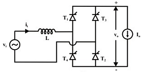
Fig. Circuit Diagram
During this period the load current freewheels through the thyristors and the output voltage is clamped to zero. On the other hand, the input current starts changing polarity as the current through T1 and T2 increases and T3 T4 current decreases. At the end of the overlap interval the current through T3 and T4 becomes zero and they commutate, T1 and T2 starts conducting the full load current. The same process repeats during commutation from T1 T2 to T3T4 at ωt = π + α.
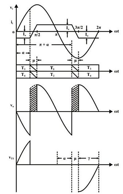
Fig. Waveform
From Fig. Above it is clear that, commutation overlap not only reduces average output dc voltage but also reduces the extinction angle γ which may cause commutation failure in the inverting mode of operation if α is very close to 180º. In the following analysis an expression of the overlap angle “μ” will be determined.
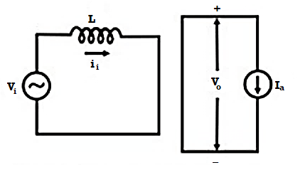
Fig. Equivalent Circuit during overlap


At 


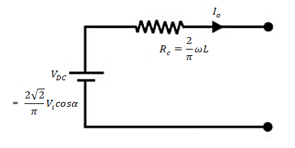
The simple equivalent circuit of Fig. Above represents the single phase fully controlled converter with source inductance as a practical dc source as far as its average behaviour is concerned. The open circuit voltage of this practical source equals the average dc output voltage of an ideal converter (without source inductance) operating at a firing angle of α. The voltage drop across the internal resistance “RC” represents the voltage lost due to overlap shown in Fig. By the hatched portion of the v0 waveform. Therefore, this is called the Commutation resistance. Although this resistance accounts for the voltage drop correctly there is no power loss associated with this resistance since the physical process of overlap does not involve any power loss. Therefore, this resistance should be used carefully where power calculation is involved
Three phase fully controlled converter with source inductance
When the source inductance is taken into account, the qualitative effects on the performance of the converter is similar to that in the case of a single phase converter. Fig. Below shows such a converter. As in the case of a single phase converter the load is assumed to be highly inductive such that the load can be replaced by a current source.
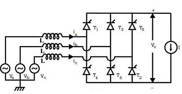
Fig. Circuit Diagram
As in the case of a single phase converter, commutations are not instantaneous due to the presence of source inductances. It takes place over an overlap period of “μ1” instead. During the overlap period three thyristors instead of two conducts. Current in the outgoing thyristor gradually decreases to zero while the incoming thyristor current increases and equals the total load current at the end of the overlap period. If the duration of the overlap period is greater than 60º four thyristors may also conduct clamping the output voltage to zero for sometime. However, this situation is not very common and will not be discussed any further in this lesson.
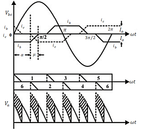
Due to the conduction of two devices during commutation either from the top group or the bottom group the instantaneous output voltage during the overlap period drops (shown by the hatched portion of Fig. Above resulting in reduced average voltage. The exact amount of this reduction can be calculated as follows. In the time interval α < ωt ≤ α + μ, T6 and T2 from the bottom group and T1 from the top group conducts. The equivalent circuit of the converter during this period is given by the circuit diagram of Fig. Below
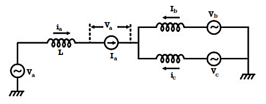
Therefore in the interval <t +
+


But 


At 


For 

For 


It should be noted that RC is a “loss less” resistance, since the overlap process does not involve any active power loss.
The input power factor is defined as the ratio of the total mean input power to the total RMS input volt-amperes.
PF = ( V1 I1 cos φ1 ) / ( Vrms Irms)
Where V1 = phase voltage
I1 = fundamental component of the supply current
φ1 = input displacement angle
Irms = supply rms current.
Pulse Width Modulation
If the output voltage of single phase half-controlled converter is controlled by delay angle, extinction angle or symmetrical, there is only one pulse per half cycle in the input current of the converter, and as a result, the lowest order harmonic is third. It is difficult to filter out the lower order harmonic current. In Pulse Width Modulation (PWM) control, the converter switches are turned on and off several times during a half cycle, and the output voltage is controlled by varying the width of pulses. The gate signals are generated by comparing a triangular wave with a dc signal as shown in Fig. Below. In this case, all the pulse widths obtained are equal. Fig. Below shows the input voltage, output voltage, and input current. The lowest order harmonic can be eliminated or reduced by selecting the number of pulses per half cycle. However, increasing the number of pulses would also increase the magnitude of higher order harmonics, which could easily be filtered out.
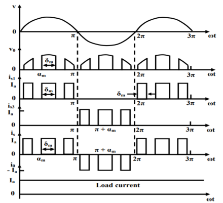
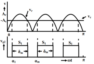
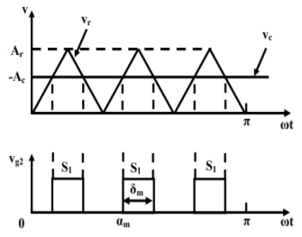
The output voltage (i.e., performance parameters) can be obtained in two steps: (i) by considering only one pair of pulses such that, if one pulse starts at 1 ωt = α, and ends at 1 t ω =α +δ1, the other pulse starts at 1 ω =π+α t , and ends at ω = π+α 1+δ 1 , then by combining the effects of all pairs of pulse. If mth pulse starts at ωt= αm and its width is δm, the average output voltage due to p number of pulses is found as

If the load current with an average value of Ia is continuous and has negligible ripple, the instantaneous input current is expressed in a Fourier series as

Due to symmetry of the input current waveform, even harmonics are absent, and Idc is zero. The Fourier coefficients are obtained as


So, the equation for is(t) is written as

Where 
Sinusoidal Pulse Width Modulation (SPWM) Control
Various types of modifications in PWM techniques have been proposed. One important method is sinusoidal pulse width modulation (SPWM) control, the pulse widths are generated by comparing a triangular reference voltage vr of amplitude Ar and frequency fr, with a carrier half sinusoidal voltage vc of variable amplitude Ac and frequency 2fs. The sinusoidal voltage vc is in phase with the input phase voltage vs and has twice the supply frequency fs. The widths of the pulses (and the output voltage) are varied by changing the amplitude Ar or the modulation index M from 0 to 1. The modulation index, M is Ac/Ar. It may be noted that the width of the pulses obtained are variable. The width is smaller at the centre of the carrier signal (sinusoidal), and increases as one goes to the start and end of the above signal. Fig. Shows the various waveforms, including the currents through thyristors and the input current and load current (assumed to be continuous).
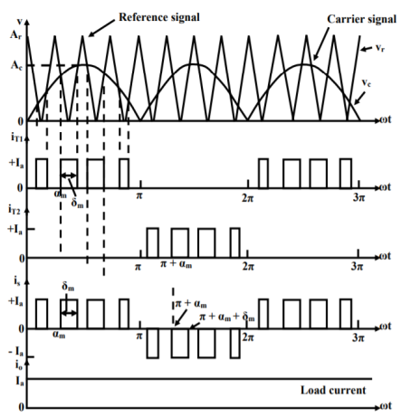
It may be noted that, in the earlier case (multiple PWM control), the pulse widths are uniform (equal). In this type of control, the displacement factor is unity, and the power factor is improved. The lower order harmonics one eliminated or reduced. For example, width four pulses per half cycle, the lowest order harmonic is the fifth, and so on. Different modifications have been suggested to take one such example, as the pulse width one small in the centre as shown in Fig., the carrier signal is modified to care of this. The triangular waveforms are kept same, upto some point from the start and end of the cycle, and then the pulse widths can be made uniform.
So, the power factor is improved with various control methods discussed. For different PWM methods used, the harmonic components of the voltage waveforms are also decreased or eliminated.
Three phase full converter
It is a fully controlled bridge controlled rectifier using six thyristors connected in the form of a full wave bridge configuration.
All the six thyristors are controlled switches which are turned on at a appropriate times by applying suitable gate trigger signals.
The three phase full converter is extensively used in industrial power applications up to about 120kW output power level, where two quadrant operations is required.
The figure shows a with highly inductive load. This circuit is also known as three phase full wave bridge or as a six pulse converter.
The thyristor are triggered at an interval of (∏/3) radians (i.e. at an interval of 30°). The frequency of output ripple voltage is 6fs and the filtering requirement is less than that of three phase semi and half wave converters.
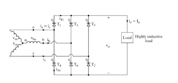
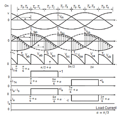
- At ωt=(∏/6 +α) , thyristor is already conducting when the thyristor is turned on by applying the gating signal to the gate of . During the time period ωt=(∏/6 +α) to (∏/2 +α), thyristors and conduct together and the line to line supply voltage appears across the load.
- At ωt=(∏/2 +α), the thyristor T2 is triggered and T6 is reverse biased immediately and T6 turns off due to natural commutation. During the time period ωt=(∏/ +α) to (5∏/6 +α), thyristor T1 and T2 conduct together and the line to line supply voltage appears across the load.
- The thyristors are numbered in the circuit diagram corresponding to the order in which they are triggered. The trigger sequence (firing sequence) of the thyristors is 12, 23, 34, 45, 56, 61, 12, 23, and so on.
- The figure shows the waveforms of three phase input supply voltages, output voltage, the thyristor current through T1 and T4, the supply current through the line ‘a’.
- We define three line neutral voltages (3 phase voltages) as follows
Vrn = Van = Vm sinwt ; Vm= max phase voltage.
Vyn = Vbn = Vm sin(wt - 2π/3) = Vm sin(wt-120)
Vbn = Vcn = Vm sin(wt + 2π/3) = Vm sin(wt + 120) =Vm sin(wt -240)
Where Vm peak phase voltage of star (Y) is the connected source.
The corresponding line to line voltage are
Vry=Vab = (van –vbn) =  Vm sin(wt +
Vyb = Vbc = (vbn – vcn) =  Vm sin(wt -
Vbr = Vca = (vcn-van) =  Vm sin(wt +
The electric energy conversion made by semiconducting converters is being used more and more. This had led to the growth of negative phenomena, that appeared negligible, when only a few converters being used. However, the development of semiconductor structures has enabled higher power to be transmitted and has also led to wide spread of converters. In this way, converters have a negative effect on the supply network. The regressive effects of overloads with harmonics and reactive power consumption are becoming major disadvantages of phase controlled (mostly thyristor) rectifiers. These side effects need to be compensated by additional filtering circuits with capacitors or inductances. However, such circuits raise the costs and also increase material and space requirements for the converter. Phase control and commutation of semiconducting devices impact the phase displacement between the first harmonics of the consumed current and the first harmonics of the supply voltage. This displacement leads to power factor degradation and to reactive power consumption. The consumed current harmonics cause non-sinusoidal voltage drops on the supply network impedances and lead to supply voltage deformation. This may cause malfunctions of other devices that are sensible to the sinusoidal shape of the supply voltage (e.g. Measurement apparatuses, communication and control systems). The reactive power rises with longer control angle delays, so the rectifier acts as a time variable impedance that is nonlinear and causes deformed current consumption.
PWM Rectifier
In order to suppress these negative phenomena caused by the power rectifiers, use is made of rectifiers with a more sophisticated control algorithm. Such rectifiers are realized by semiconductors that can be switched off IGBT transistors. The rectifier is controlled by pulse width modulation. A rectifier controlled in this way consumes current of required shape, which is mostly sinusoidal. It works with a given phase displacement between the consumed current and the supply voltage. The power factor can also be controlled and there are minimal effects on the supply network. PWM rectifiers can be divided into two groups according to power circuit connection – the current and the voltage type. For proper function of current a type rectifier, the maximum value of the supply voltage must be higher than the value of the rectified voltage. The main advantage is that the rectified voltage is regulated from zero. They are suitable for work with DC loads (DC motors, current inverters) For proper function voltage type rectifiers require higher voltage on the DC side than the maximum value of the supply voltage.
The rectified voltage on the output is smoother than the output voltage of the current type rectifier. They also require a more powerful microprocessor for their control. Output voltage lower than the voltage on input side can be obtained only with increased reactive power consumption. The function of the rectifier depends on the supply type of network. There are two types of supply network – “hard” and “soft”. Ordinary rectifiers, which work on a relatively “hard” supply network, do not affect the shape of the supply voltage waveform. Harmonics produce electromagnetic distortion, and the network will be loaded with reactive power. The PWM rectifier aims to consume sinusoidal current and to work with given power factor. A PWM rectifier connected to the “soft” supply network has more potential to affect the shape of the supply voltage network. It can be controlled, so the current consumed by the PWM rectifier will partly compensate the non-harmonic consumption of other devices connected to the supply network
Control of PWM Rectifier
The basic block diagram of one phase PWM rectifier is shown in Figure below. The rectifier consists of 4 IGBT transistors, which form a full bridge, the input inductance and the capacitor at the output. It is controlled by pulse width modulation. Supply voltage Us and the voltage at the rectifier input Ur are sinusoidal waveforms separated by the input inductance.
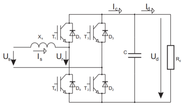
Figure. PWM rectifier using IGBT
The energy flow therefore depends on the angle between these two phasors. See the phasor diagram in Figure below.
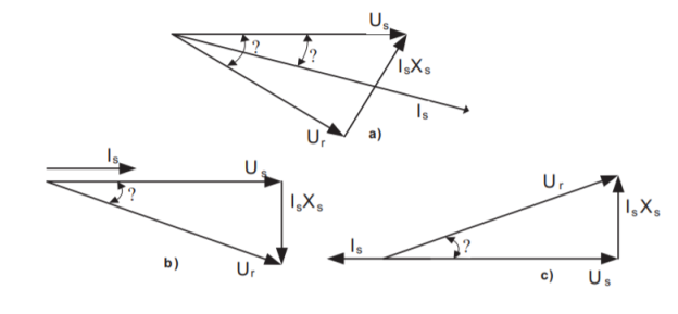
Figure. Phasor diagrams
The power transferred from the supply to the input terminals of the rectifier is
PSR = (UsUr/Xs) sin  = Us Is sin
Where:
- Us RMS value of input supply voltage (V),
- Ur RMS value of first harmonics consumed by AC rectifier input (V),
 phase displacement between phasors Us a Ur,
- Xs input inductor reactance at 50Hz,
- ɸ power factor
In order to make the rectified voltage constant, the input and output powers must be balanced. Then, as the phasor diagram in Figure above.
Is cos ɸ= Ur sin  /Xs
/Xs
Is sin ɸ = Us- Ur cos  /Xs
/Xs
As long as the reactive power consumed is equal to zero, the power factor is equal to unity.
Is Xs = Ur sin 
Us = Ur cos 
Phasor diagrams of the rectifier, which works both, as a rectifier, and as an inverter, are shown in Figs. b and c. The aim is to control the rectifier in such a way that it consumes harmonical current from the supply network, which is in phase with the supply voltage.
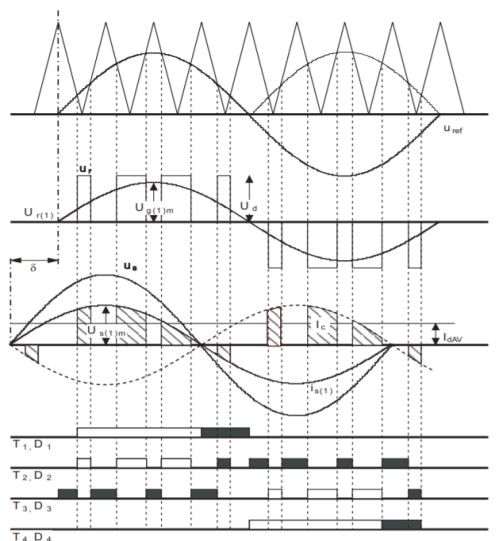
Fig. Voltage and current waveforms in a PWM rectifier
This can be achieved by controlling the rectifier in one of a number of ways, e.g., by pulse width modulation. Voltage and current under this control are shown in Figure. One possible way of transistor switching is shown at the bottom of Fig. It can be seen that two states alternate. First, the current flows into the load (D1 and D2 conducts), and second, the input of the rectifier is short circuited (D1 and T3 conducts). The grey areas mean that the transistor conducts. The white areas mean, that the passive element conducts. The transistor is turned off and the current flows through the antiparallel diode. The switching of devices must be precisely synchronized with the supply voltage.
The output voltage of the rectifier Ud is usually controlled to a constant value by using another converter e.g. An inverter. It is therefore possible, at a given current Id at the converter output, to assign to output voltage Ud a particular value of z and  . If we consider cos ɸ= 1and the power equality on the AC and DC side can be written as:
Id= [z. Is(1)m /2 ]cos 
Is(1)m = 2UdAV IdAV/Usm
 = arctan
  L Is(1)m/Usm
Ug(1)m = Usm/ cos 
The rectifier controller can be made on the basis of these equations. It is obvious that only two variables are needed for such rectifier control. Firstly, the displacement angle  must be controlled and the other necessary variable is z,
z= uref/upil
Which is defined as the ratio of the modulation signal uref amplitude to the saw-voltage upil amplitude. During displacement angle control, it is necessary to consider, that if increases the current through the inductance, will also increase. For proper rectifier function, it is also necessary to synchronize the control algorithm with the supply voltage. By detecting the zero crossing, the controller controls the displacement angle. The synchronization circuit must be very accurate and also fast and reliable.
Pulse width modulation rectifiers (PWM) have arisen as a solution to overcome these problems, reducing harmonic pollution and adapting in accordance to the highest requirements for energy quality. Using these devices, it is possible to control the output voltage and to obtain sinusoidal ac currents. In order to assess the performance of a three-phase PWM rectifier, two parameters are taken into account: the Total Harmonic Distortion (THD), which is a measurement of the harmonic content of the current signal; and the Power Factor (PF), which accounts for phase differences between the current and the voltage. With this thread in mind, PWM rectifiers seek a unity PF and a small THD. Several strategies have been proposed to control three phase PWM rectifiers. In the reported research, multiple Proportional Integral controllers have been implemented in the current loops, mainly due to the ease of implementing them as well as their satisfactory performance. However, the main limitation of this approach lies in an inherent tracking (amplitude and phase) error. Over the last few years, interesting emerging control techniques such as resonant control and repetitive control (RC) have been developed to track/reject periodic signals. Good response characteristics are achieved by using these strategies, ensuring near unit power factor and constant output dc voltage under parameter uncertainties, as well as load disturbances. The main disadvantage is related to the lost of performance caused by variations of the network frequency from its nominal value.
Three-phase PWM rectifier
PWM techniques have been widely implemented to control the output of power converters as they allow shaping voltage and/or current waves based on specific applications
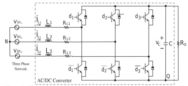
Figure. Three-phase pulse width-modulated (PWM) rectifier.
The three-phase PWM rectifier circuit, as shown in Figure, has three-legs with IGBT transistors. It is known as a bidirectional boost rectifier (increasing the voltage) and works using fixed DC voltage polarity. Input inductors are an integral part of the rectifier and are selected based on their design. We achieve harmonic compensation through the input inductors, and we ensure smooth voltage waveforms by using capacitors. The dynamics of the three-phase PWM rectifier


Where Ln, C and Ro are the nominal values of inductances, the capacitor and the load resistance, respectively; iL1, iL2 and iL3 are the phase currents and Vc is the capacitor voltage; Vin1, Vin2 and Vin3 are the known three-phase sinusoidal voltages; Vin1+Vin2+Vin3=0; RLn is the parasitic inductor resistance for each phase
VQN = - (d1 + d2 + d3)
And dn is the control action used to trigger the IGBTs. Their values range within the interval [0,1].
1. IGBT is a voltage control device, which means when a voltage applied to its gate terminal it will start conducting current, it does not consume any current in its gate terminal. On the other hand, SCR is a current-controlled device, which means it consumes some current through its gate terminal to operate.
2. The gate terminal of the IGBT is isolated, so it gives a very high safety when operating at high voltage, on the other hand, in the SCR the gate terminal is not insulated.
3. IGBT has electronic signal amplifying capability whereas SCR does not have amplifying capability.
4. An extra arrangement or method is required to turn off the SCR. On the other hand, IGBT does not require any special method for turning off.
5. SCRs are most suitable for fast switching and low power applications compared to IGBTs whereas IGBT mostly used in high power circuits.
6. SCRs are used in rectifier circuits, inverter circuits, timing circuits, light-dimming circuits whereas IGBTs are used in High Power Motor Driver Circuits, High Power Inverter circuits.
References:
- Power Electronics by Muhammad H Rashid
- Power Electronics by Evolution, Technology and applications by A.K.Bose