Unit - 3
DC to AC Converters
Single Phase bridge inverter
Alternating current (AC) power supply is used for commercial and industrial needs. However the issue arises that AC cannot be stored for future use. So AC is converted to DC and stored in batteries or sometimes in ultra-capacitors.
So, whenever AC is needed DC is converted to AC and used for AC based applications. So the device which converters DC into AC is called inverter.
For single phase applications, single phase inverter is used. There are mainly two types of single-phase inverter: Half Bridge Inverter and Full Bridge Inverter.
Half Bridge Inverter
This type of Inverter requires two power electronics switches (MOSFET). The MOSFET or IGBT is used for switching purpose. Circuit diagram of the half bridge inverter is as shown in below figure.
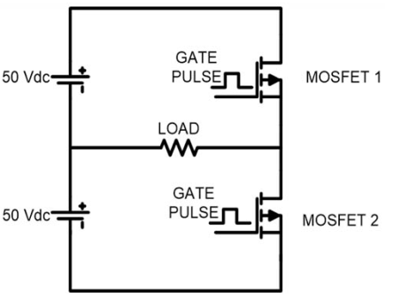
As shown in circuit diagram, input DC voltage is Vdc = 100 V. This source is divided into two equal parts. The gate pulses are given to the MOSFET as shown in below figure.
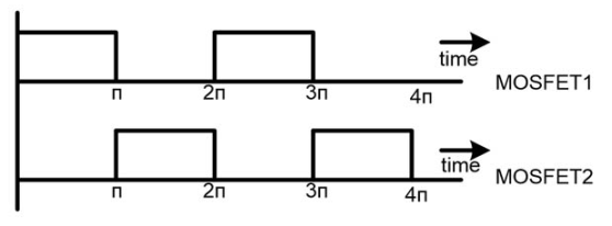
The time period of one cycle (0 < t < 2π) is 20msec.
First half cycle:
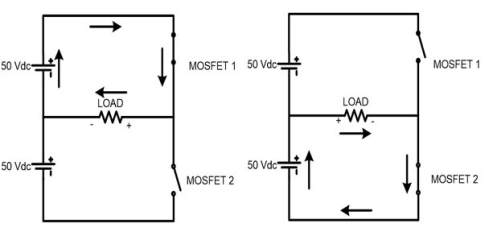
MOSFET-1 is triggered for first half cycle (0 < t < π) and during this time period MOSFET-2 is not triggered. In this period, current will flow in the direction of arrow as shown in below figure and half cycle of AC output is completed. The current from the load is right to left and load voltage is equal to +Vdc/2.
In second half cycle (π < t < 2π)
MOSFET-2 is triggered and lower voltage source is connected with the load. The current from the load is left to right direction and load voltage is equal to -Vdc/2. In this time period, current will flow as shown in figure and the other half cycle of AC output is completed.
Full Bridge Inverter
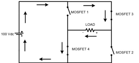
In this type of inverter, four switches are used. In full bridge inverter, peak voltage is same as the DC supply voltage. The circuit diagram of full bridge inverter is as shown in the figure below.
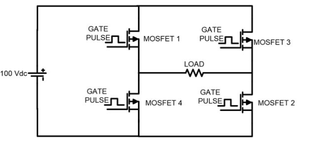
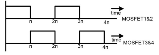
The gate pulse for MOSFET 1 and 2 are same. Both switches are operating at same time. Similarly, MOSFET 3 and 4 has same gate pulses and operating at same time.
But, MOSFET 1 and 4 (vertical arm) never operate at same time. If this happens, then DC voltage source will be short-circuited.
For upper half cycle (0 < t < π)
MOSFET 1 and 2 get triggered and current will flow as shown in figure below. In this time period, the current will flow from left to right direction.
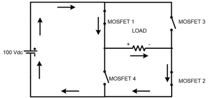
Upper Half cycle
For lower half cycle (π < t < 2π)
MOSFET 3 and 4 get triggered and current will flow as shown in figure. In this time period, the current flow from right to left direction. The peak load voltage is same as DC supply voltage Vdc in both cases.
Expression
The instantaneous output voltage can be expressed in Fourier Series as
Vo = a0/2 +  n cos(nwt) + bn sin(nwt) ---------------(1)
Due to square wave symmetry along the x-axis both a o and an are zero, and bn is obtained as
Bn = 1/π [  d(wt) +
  -----------------------(2)
Substituting the value of bn from equation 2 into equation 1 gives the instantaneous output voltage
Vo =  sin(nwt) -------------------------------(3)
The instantaneous current through the resistive load is given by
iL =  sin(nwt) ------------------------------(4)
Single-phase half-bridge inverter with an RL load
- For the half-bridge inverter circuit, the centre-tap of the DC supply is used as one of the load terminals. The centre-tap is created by the two series-connected equal valued capacitors across the DC supply.
- The two switches, T1 and T2, are switched alternately, in a complementary fashion, at the desired output frequency fo.
- When T1 is ON, T2 is OFF and the voltage at the terminal A of the load is +Vd/ 2 V, irrespective of the direction of current through the load.
- Similarly, when T2 is ON, the T1 is OFF and the potential at point A is -Vd /2 .
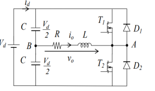
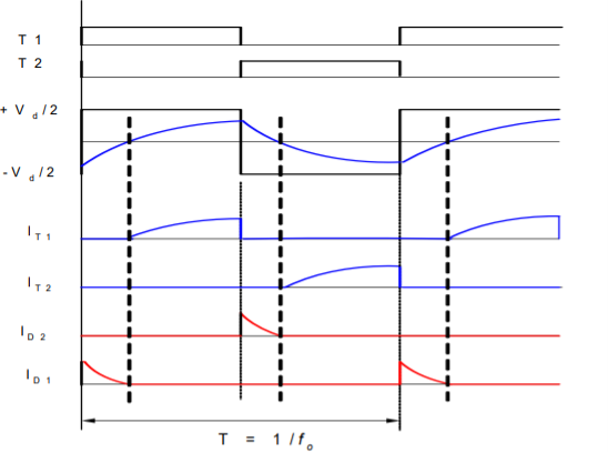
- The load voltage is a square-wave of amplitude Vd/2 and the load current waveform is exponentially rising and falling waveform determined by the load impedance.
- For a resistive load the current waveform follows the voltage waveform.
- For an inductive load the current waveform lags the voltage waveform by an angle which is, approximately, the load power factor angle.
- When the switch T1 is switched off, the load current is at its positive peak, and it will continue to flow through the diode D2 back into the lower capacitor across the DC source.
- The conducting diode D2 will reverse bias the transistor T2 (from collector to emitter) until the load current falls to zero.
- Thereafter, the transistor T2 will be forward biased and negative current will establish in the load through T2.
- Similarly, diode D1 conducts when T2 is switched OFF and T1 starts to conduct when the load current rises to zero. Diodes D1 and D2 carry currents which are due to the trapped energy in the load inductor.
- Consequently, these diodes are referred to as reactive feedback diodes which return the load reactive power back to the DC source. These diodes are also necessary to allow a path for the current to flow when a transistor is turned off, thus protecting the switches against the overvoltage that would be created by a sudden turn-off of current in the load inductance.
Single-phase full-bridge inverter with RL load
In this circuit four switches are used and the DC supply centre-tap is not required. Switches T1 and T2 are switched together while switches T3 and T4 are switched together alternately to T1 and T2 in a complementary manner. The four feedback diodes D1-D4 conduct currents as indicated in the figure below.
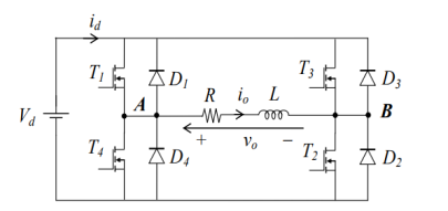
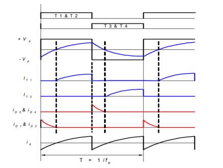
The output load voltage alternates between +Vd when T1 and T2 are on and -Vd when T3 and T4 are on, irrespective of the direction of current flow. It is assumed that the load current does not become discontinuous at any time.
The output RMS voltage
Vo = [2/T  2 d dt ] ½ = Vd ---------------------(1)
Vo =  sin nwt ---------------------------------(2)
The fundamental RMS output voltage
V1 = 4Vd/ = 0.9 Vd ------------------------------------(3)
When the switches T1 and T2 are on load current increases exponentially according to
Vd = L di/dt + Ri
Solving this
i = A e –(R/L)t + Vd/R ---------------------------------------------(4)
Assuming that at t=0 the initial current is Io , the solution for i is
i= Vd/R + (Io – Vd/R) . e –(R/L) t ----------------------------------------------(5)
Where 0≤ t ≤ t1 , t1 being the end of the period for T1 and T2 .
At the end of the on period for T1 and T2 i0 is at maximum and diodes D3 and D4 start conduction. T3 and T4 are reversed biased by these diodes. The load current now falls according to
-Vd = L di/dt + Ri --------------------------------------------------(6)
The solution of this equation is
i = - Vd/R + (I1 + Vd/R) . e –(R/L) t2 ---------------------------(7)
Where 0≤ t2 ≤ t2-t1, t2 being 0 at t1, and I1 is the current at the end of the ON period of T1 and T2.
In the steady state I1 = -Io. The steady-state value of I1 can be found by solving 5 and 7 simultaneously. I1 in closed form is given by
I1 = Vd/R = [1 – e (R/L) t1]/[1+ e (R/L)t1]---------------------------------------(8)
The zero current crosses over the point tx is found from eq(5) from the condition that at t=tx , i=0. This gives
Tx = (L/R) ln(1- R/Vd)I0 sec -----------------------------(9)
The steady mean output power to the load is given by
P = 1/t1  watts.-----------------------------------(10)
Performance Parameters
Harmonic factor of nth harmonic, HFn
It is a measure of individual harmonic contribution. HFn versus the control parameter gives the harmonic profile of the inverter. Small HFn value is desired.
HFn = Von/Vol for n>1
Total harmonic distortion, THD
It is a measure of closeness in shape between a waveform and its fundamental component (sinusoidal waveform). THD = 0 means sinusoidal wave.
THD = 1/V01  2 on ]1/2
Distortion Factor, DF
DF indicates the amount of HD that remains in a particular waveform after the harmonics of that waveform have been subjected to the second order attenuation (i.e. divided by n2)
DF of nth harmonic component, DFn
DFn = Von / Vo1 n2 for n>1
Lowest-order harmonic LOH
LOH is that harmonic component whose frequency is closest to the fundamental one. Its amplitude is normally > 3% of the fundamental component. High LOH is desired.
LOH ≥ 3 % x V01
Examples
Q1) (a) A single-phase full bridge inverter is connected to an RL load. For a dc source voltage of  and output frequency
  , obtain expressions for load current as a function of time for the first two half cycles of the output voltage.
(b) Derive also the expressions for steady-state current for the first two half cycles.
(c) For R=20 and L=0.1 H, obtain current expressions for parts (a) and (b) in case source voltage is 240 V dc and frequency of output voltage is 50 Hz.
A1)
(a) For the first half cycle, ie for 0<t<t/2, the voltageequation for RL load is

Its Laplace transform, with zero initial conditions, is

Its time solution is
 for 0<t<T/2
This is the expression of current as a function of time for the first half cycle from the instant of switching in with  at
at 
At  current
  becomes the initial value for second half cycle

For second half cycle, time limit is from T/2 to T or 0 <t’< T/2 where  . The voltage equation for RL load dring second half cycle is

Its Laplace transform with initial current  given by


Its time solution is 


The transient solution for load current for first and second half cycles respectively.
(b) Under steady-state conditions at t=0,  , Under this condition,
Laplace transform

Its time solution is 
The steady-state solution during the second half cycle, ie for 0<t’ <T/2 where t’ =t-T/2
(c) Here 
Expression for transient current during the first half cycle form os

Expression for transient current during the second half cycle


Steady-state current for the first half cycle, ie for 0<t<T/2


For the second half cycle, steady state current

Q2) A single-phase bridge inverter delivers power to a series connected RLC load with R=2 and L=10. The periodic time T=0.1 msec. What value of C should te=he load have in order to obtain load commutation for the SCRs. The thyistor turn-off time is 10sec. Take circuit turn off time as 1.5 . Assume that load current contains only fundamental component.
A2) The value of C should be such that RLC load is underdamped. Moreover when load voltage passes through zero, the load current must pass through zero before the voltage wave, ie the load current must lead the voltage by angle θ as shown in fig 8.6 recall the phasor diagram for RLC series circuit. From his phasor diagram,
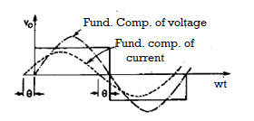

Here  as the current is leading the voltage. Now
  must be at least equal to circuit turn-off time ie 1.5×10=15 sec


The condition when the inverter has the risk of getting damaged is called as cross conduction. In half bridge and full bridge converter we usually see this condition. The figure shown below has Q1 and Q2 being turned on at same time and hence acts as short circuit through the supply. As both starts conducting at the same time causes high amount of current to flow in the device. This sudden high value of current may damage the circuit.
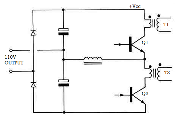
Figure. Half-Bridge Circuit
In normal case both the transistors will not conduct as the same moment. The cause of cross conduction can be traced to excessive storage time in the switching transistor. The below waveform shows that in between time interval t1-t3 cross conduction will occur.
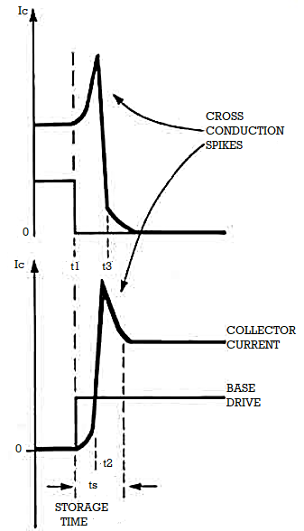
Figure. Cross-Conduction waveform
Basically, only one transistor is made to conduct at particular period of time. The above waveform shows Q1 is removed at t1 time. But the transistor has some storage time which allows he current to pass through the collector and hence taking additional time till t3. The Q2 turns on at this time. The turn on delay is less than the storage time in normal bipolar transistor. Hence, for the time interval t2-t3 both transistors conduct. Since, they are directly across the supply line the low source impedance allows very large collector currents to flow.
If no current limiting is provided for the above case and also if source impedance of supply line is very low, then large cross conduction currents will flow through Q1 and Q2 causing failure of transistors.
Prevention of Cross Conduction
In order to prevent the cross conduction a dead time is provided between the two pulses. This dead time is chosen such that on time of both transistors do not overlap. There is considerable variation in the storage times of apparently similar devices. Also, the storage time is a function of temperature, drive circuit, and collector current loading. Hence, to ensure an adequate safety margin, the dead time will need to be considerable, and this will reduce the efficiency and the range of pulse-width control.
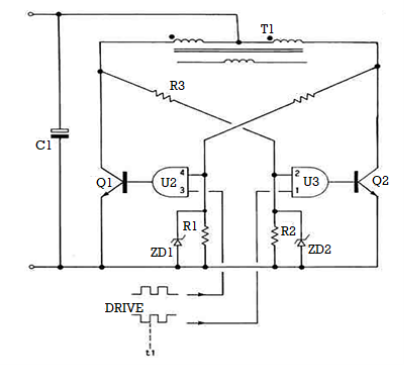
Fig. Cross-coupled cross-conduction inhibit circuit
The push-pull converter is taken as example for cross coupling to prevent cross conduction. When both Q1 and Q2 are turned on at same instance transformer T2 will be short circuited. The AND gates U2 and U3 prevent the cross conduction.
It has already been mentioned that Inverter Control providing a variable frequency supply to three phase motors should be capable of providing a variable voltage. This is required to avoid saturation and ensure operation at constant flux density. The Voltage Control Techniques for Inverters can be affected either external to the Inverter Control or within it.
The Voltage Control Techniques for Inverters can be done in two ways.
- By varying the dc link voltage
- By varying the ac voltage at the output using a variable ratio transform
The variation in dc link voltage can be achieved in many ways. It has the advantage that the output voltage waveform is maintained over a wide range of frequencies. But at very low frequencies, the dc link voltage may be too low to commutate the inverter. This limits the lowest operating frequency and hence the frequency range. The dynamic response is also poor.
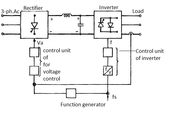
Fig. Inverter control for variable link voltage
A variable dc supply can be obtained by using a phase controlled rectifier on the line side. A closed loop control varies the firing angle depending upon the frequency. The function generator gives a relation between the stator frequency and applied voltage to the stator for constant air gap flux or given flux conditions in the motor. The output of the function generator is voltage for a given value of fs. This voltage is compared with the measured value of voltage and the error so obtained is used to change the firing angle of the converter on the line side. The frequency is obtained by controlling the firing and conduction of the thyristors of the machine side converter. A current loop is also employed to limit the current to safe values during dynamic operation of the system.
A combination of a diode rectifier and a dc chopper is used for varying the dc link voltage. Closed loop control in this case changes the time ratio of the chopper. Yet another way is to use a variable ratio transformer which operates at constant frequency, before the diode rectifier.
The Voltage Control Techniques for Inverters Control can be affected by means of a variable ratio transformer interposed between the motor and inverter. The method is very simple. Even in this case the waveforms of output voltage remain the same over a wide frequency range. The line side converter can be a simple diode rectifier. This provides a good pf. The main disadvantage of this method is that the transformer has to be designed for low frequencies and its size is large. The system also has an extremely poor dynamic response.
The dc link voltage is constant and the inverter is controlled to provide-both variable voltage and variable frequency. As the link voltage is Constant a simple diode rectifier may be employed on the line side. Variable voltage variable frequency supply to the motor is obtained within the Inverter Control itself using suitable control based on the principles of PWM.
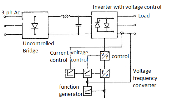
Fig. Voltage control within inverter
The block diagram of control of the constant voltage inverter is shown in Figure. The voltage is sensed and compared with the output of the function generator. The error is used to change the amplitude of the reference wave in order to obtain the desired value of voltage. The frequency of the reference wave is changed in order to get the desired frequency. As the inverter is supplied at constant voltage commutation problem at low frequencies disappears. The operating frequency extends to zero and the system has a very good dynamic response. The voltage waveform is not the same at all frequencies. At low frequencies the harmonic content may increase.
PWM techniques are very widely used. They sometimes provide harmonic elimination also. For this purpose, sinusoidal modulation is used. The principles of PWM are illustrated in Fig.
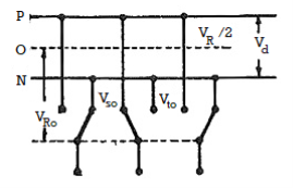
Fig. PWM technique
When there are AC loads it requires the voltage to be maintained or controlled at the input terminals. When inverters are used for such loads, we need the output voltage to be in control. Because the requirements of AC loads can be fulfilled.
(a) External control of AC output voltage:
This can be done by AC voltage control in which an ac voltage controller is connected in between the output terminals of inverter and the load. The below figure shows the connections. The voltage input to the ac load is regulated through the firing angle control of ac voltage controller. But there are harmonics in the output when the output voltage from the ac voltage controller is at low level.

The other method is series inverter method which consists of two or more inverters which are connected in series. Figure below shows that the output voltage of two inverters is summed with the help of transformer. The secondaries of the transformer is connected in series having input as the inverters output. The resultant voltage from the phasor is then

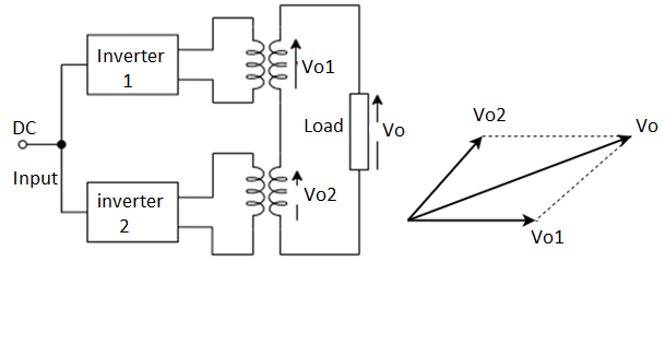
Fig. Series Inverter Control of two inverters
The essential condition for this is V01, V02 should be equal.
When  =0
=0
V0= V01+ V02
When  =π
=π
V0 = 0 only when V01= V02
As inverters are connected in series this method is also called as multiple converter control.
(b) External control of dc Input Voltage
AC voltage source is present here. The input to the converter which is dc voltage is controlled through the fully controlled rectifier (a). Alternate method is to use an uncontrolled rectifier and a chopper (b). The other way is to use an ac voltage controller and an uncontrolled rectifier (c). If the available volage is dc then dc voltage input to the inverter is controlled by means of a chopper as shown in figure below.
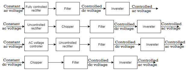
Fig. External control of dc input voltage to inverter
The output voltage waveform and its harmonics are not affected as the output voltage of inverter is controlled through the adjustment of dc input to the inverter.
(c) Internal control of Inverter
By adjusting the voltage within the inverter, the output voltage can be adjusted. The is can be achieved by pulse width modulation control (PWM). In PWM method the inverter is fed with fixed dc input voltage and a controlled ac output voltage is obtained by adjusting the ON and OFF periods of the inverter.
No additional components are required to adjust the voltage. The lower harmonic orders are also eliminated. The higher order harmonics can be filtered easily. The main disadvantage of this method is that the SCR are expensive as they must posses low turn on and turn off times.
Key takeaway
When there are AC loads it requires the voltage to be maintained or controlled at the input terminals. When inverters are used for such loads, we ned the output voltage to be in control. Because the requirements of AC loads can be fulfilled.
The output voltage control for inverters can be done by following methods
Single-Pulse Modulation
The output voltage from inverter is shown in below figure. When the waveform is modulated the output voltage is of the form as in figure. The width of pulse is 2d and is symmetrical about π/2 and another pulse located symmetrically about 3 π/2. The output voltage is controlled by varying the pulse width of 2d. Figure shows the output voltage waveform and is called as quasi-square wave.
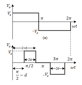
Fig. Single Pulse Modulation
The Fourier analysis will be

As waveform is symmetrical Bn =0. The output waveform will then become


When pulse width 2d is equal to maximum value of π radians, the peak value of fundamental component is [4Vs/ π] sin d. The peak value of nth harmonic is


The RMS value of output voltage is

Multiple-pulse Modulation
In this method several equidistant pulses per half cycle are used. As explained above that the pulse is considered symmetrical, pulse width is also taken half and amplitudes are same. Hence, the value of RMS value will be same as derived above. The Fourier constant are


Because of factor 2 in above equation two pulses are seen from 0 to π as shown below.

Fig. Symmetrical two pulse modulation pertaining to Multiple pulse modulation.

The above waveform will be expressed in the form


The amplitude of nth harmonic of the two-pulse waveform will be

The peak value of fundamental voltage component is given as

For two-pulse modulation and pulse width d =360 for
for  = π or d= 2 π/n


For N pulse per half cycle there are N+1 intervening equidistant spaces. For v0 = 0. Total width of N+1 equidistant spaces= (N+1) Θ1
Θ1 = (π-2d)/(N+1)
From above figure Θ2 = d/N. But

Peak value of fundamental voltage component will be

The fundamental component of output voltage is lower for two pulse modulation than it is for single pulse modulation. The symmetrical modulated wave can be generated by comparing an adjustable square voltage Vr of frequency ω with a triangular carrier wave Vc of frequency ωc is shown below.
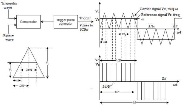
Fig. Output voltage waveform
The triggering pulses for thyristors are generated at the point of intersection of the carrier and reference signal wave. The firing pulse generated turns on the SCR making the output voltage V0. This voltage is available during the interval when the triangular wave exceeds the square modulating wave. From above figure
For triangular carrier wave, pulse width = 1/fc
For square reference wave, width of half cycle = 1/2f
Number of pulses/half cycle = [Length of half-cycle of square reference wave/Width of one cycle of triangular carrier wave]

From above figure the pulse width 2d/N is given by


The pulse width is

In this method lower order harmonics can be eliminated by proper choice od 2d and  .
.

The high frequency harmonics if present in the output can be removed by using low-size filters. But to remove the lower order harmonics the size of filter increases. So, we require some other means to remove the lower order harmonics. The methods which can be implemented are explained below.
Harmonic Reduction by PWM
The method is already discussed above where there are several pulses per half cycle. Consider the waveform shown in figure below. Which is symmetrical about π as well as π/2.
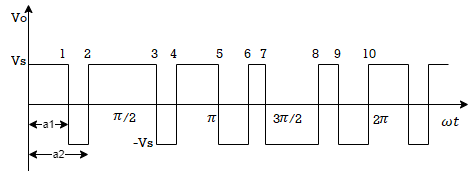
Fig. Harmonic reduction by PWM
The equation for this voltage will be

The third and fifth harmonics are eliminated


The above two equations can be solved in order to calculate α1, α2 under the condition that 0< α1<900 and α1< α2<900


The amplitude of the fundamental component for these values of α1and α2 are

The amplitude of fundamental component of unmodulated output voltage wave is

The amplitude of the fundamental voltage is 0.8391 times the amplitude of fundamental components of unmodulated voltage wave.
Harmonic Reduction by Transformer connections
The output voltage of the two or more inverters can be combined by means of transformers to get a net output voltage with reduced harmonic content. The necessary condition for this method is that the output voltage waveform from the inverter must be similar but phase shifted from each other. The output voltage v01 and v02 from inverter 1 and 2 respectively is shown below. The resultant v0 is obtained by adding vertical ordinates of v01 and v02.
The amplitude of V0 is 2Vs from interval π/3 to π and 4π/3 to 2π and so on.
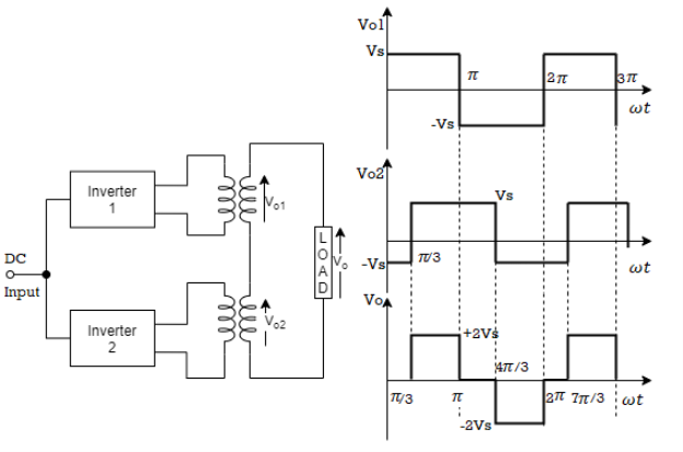
Fig(a) Harmonic reduction by transformer connections (b) Elimination of harmonics
The Fourier Series for above waveform will be given as


The voltage v0 is
V0 = v01+v02

From above equation we can say that V01 leads 600 by V02 shown in figure below. The resultant of V01 and V02 should be √3 times V01 at the same time. For third harmonics V02 lags V01 by 1800 therefore the resultant is zero.

Fig. Phasor Diagram
For fifth harmonic V02 lags V01 by 3000 its resultant is √3 times V01or V02 and it leads V01 by 300. The resultant of fifth harmonic must be associated with √3 sin(ωt+π/6). In same manner the resultant of seventh harmonic is associated with √3 sin(ωt-π/6). The fundamental component of v0 is

When there is no phase shift between the output of two inverters then the amplitude of fundamental voltage is 8Vs/π. The disadvantage of this method is we need a greater number of inverters and transformers for similar ratings.
Harmonic reduction by Stepped wave Inverters
We use pulses of different widths and heights to produce a resultant stepped wave with reduced harmonic content. From figure below we see there are two stepped wave inverters fed from a common dc source. The turn ratio of both the transformers used is different. Assuming turn ratio from primary to secondary as 3 for transformer 1 and unity for transformer 2.
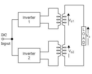
Fig. Harmonic reduction by stepped wave inverter
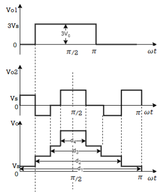
Fig. Waveform of stepped wave inverter
Let output of inverter I be v01. The output voltage level in first half cycle is either zero or positive. In negative half it can be either zero or negative. The output voltage waveform is called as two-level modulation. The output voltage of inverter II is v02. The output of this inverter is either zero, positive or negative and hence it is called as three level modulation. The resultant output voltage from a series combination of inverters I and II is obtained by superimposing the waveform as shown in figure above.
Key takeaway
The high frequency harmonics if present in the output can be removed by using low-size filters. But to remove the lower order harmonics the size of filter increases. So, we require some other means to remove the lower order harmonics. The methods used are
(i) Harmonic reduction by PWM
(ii) Harmonic reduction by Transformer connections
Harmonic reduction by Stepped wave Inverter
Three Phase voltage source inverter for balanced star
When three single-phase inverters are connected in parallel a three phase inverter is formed. The gating signal has to be displaced by 120 0 with respect to each other so as achieve three phase balanced voltages. A 3-phase output can be achieved from a configuration of six transistors and six diodes.
Two type of control signal can be applied to transistors, they are such as 180 0 or 120 0 conduction.
180 0 conduction
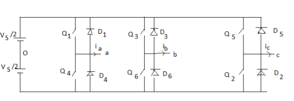
When 𝑄1 is switched on, terminal a is connected to the positive terminal of dc input voltage. When 𝑄4 is switched on terminal a is brought to negative terminal of the dc source.
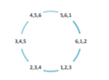
The 6 modes of operation is a cycle and the duration of each mode is 600 . The conduction sequence of transistors is 123,234,345,456,561,612. The gating signals are shifted from each other by 600 to get 3-𝜑 balanced voltages.

Switching states for the three phase voltage inverters
VRN | VYN | VBN | VRY | VYB | VBR | V1 |
V/3 | -2V/3 | V/3 | Vac | -Vdc | 0 | 2/  |
2V/3 | -V/3 | -V/3 | Vda | 0 | -Vdc | 2/  |
V/3 | V/3 | -2V/3 | 0 | V | -V | 2/  |
-V/3 | 2V/3 | -V/3 | -V | V | 0 | 2/  |
-2V/3 | V/3 | V/3 | -V | 0 | 0 | 2/  |
-V/3 | -V/3 | 2V/3 | 0 | -V | 0 | 2/  |
Fourier Analysis:
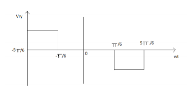
Considering the harmonic analysis
VRY =  sin nπ/3 sin n(wt + π/6)
V YB =  sin nπ/3 sin n(wt - π/2)
V BR =  sin nπ/3 sin n(wt - π/6)
All even harmonics are zero all triple n harmonics are zero.
The rms nth component of the line voltage is = 4𝑉 √2𝑛𝜋 sin𝑛𝜋/3 = 4𝑉 √2𝜋 sin(60)
For n=1 =0.7797𝑉s.
Three phase 120 0mode
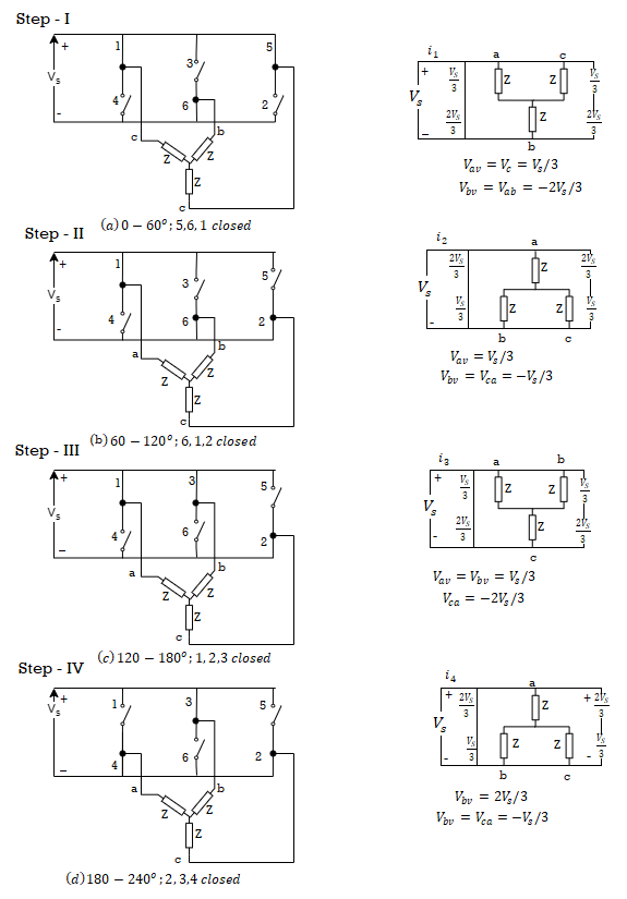
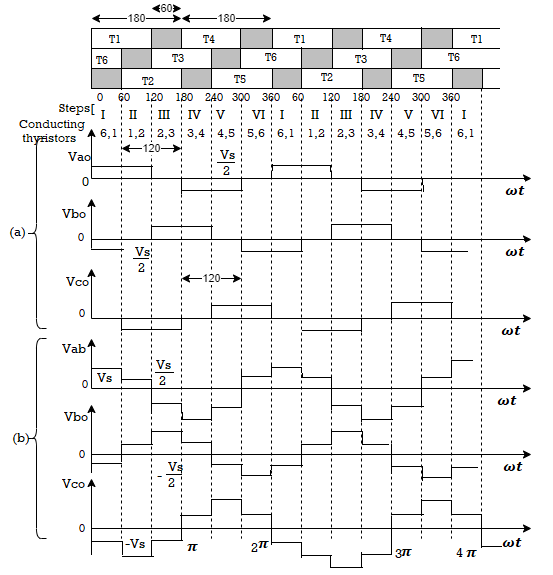
The circuit diagram is same as that for 180 0 mode of conduction. Here each thyristor conducts for 120 There are 6 steps each of 60 0 duration, for completing one cycle of ac output voltage.
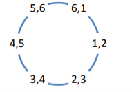
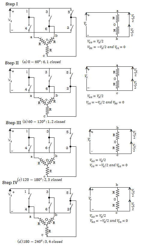
Step 1: 6,1 conducting
𝑉𝑎𝑛 = 𝑉𝑆/ 2 , 𝑉𝑦𝑛 = −𝑉𝑆 2 , 𝑉𝑐𝑛=0
Step 2: 1,2 conducting
𝑉𝑎𝑛 = 𝑉𝑆 /2 , 𝑉𝑏𝑛 = 0, 𝑉𝑐𝑛= −𝑉𝑆 /2
Step 3: 2,3 conducting
𝑉𝑎𝑛 =0, 𝑉𝑏𝑛= 𝑉𝑆/ 2 , 𝑉𝑐𝑛= −𝑉𝑆/ 2
Step 4: 3,4 conducting
𝑉𝑎𝑛 = −𝑉𝑆/ 2 , 𝑉𝑏𝑛= 𝑉𝑆/ 2 , 𝑉𝑐𝑛=0
Step 5: 4,5 conducting
𝑉𝑎𝑛== −𝑉𝑆/ 2 , 𝑉𝑦𝑛 = 0, 𝑉𝑏𝑛 = 𝑉𝑆/ 2
Step 6: 5,6 conducting
𝑉𝑎𝑛=0, 𝑉𝑏𝑛 = −𝑉𝑆 /2 , 𝑉𝑐𝑛= 𝑉𝑆 /2
120 conduction mode.
Step | Thyristor Conducting | VRn | VYn | VBn | V |
1 | 6,1 | Vs/2 | -Vs/2 | 0 |  |
2 | 1,2 | Vs/2 | 0 | -Vs/2 |  |
3 | 2,3 | 0 | Vs/2 | -Vs/2 |  |
4 | 3,4 | -Vs/2 | Vs/2 | 0 |  |
5 | 4,5 | -Vs/2 | 0 | Vs/2 |  |
6 | 5,6 | 0 | -Vs/2 | Vs/2 |  |
Utilization factor = maximum load/ installed capacity
Harmonics elimination modulation technique
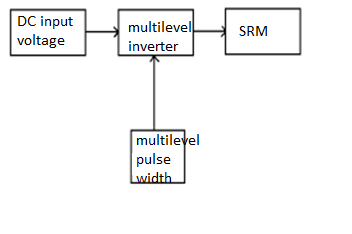
Fig. Block diagram of the general multilevel inverter
Multilevel inverters are differ from the ordinary inverter where only two levels are generated. The semiconductor devices are not connected in series to form one single high-voltage switch. In which each group of devices contribute to a step in the output voltage waveform. The steps are increased to obtain an almost sinusoidal waveform. The number of switches involved is increased for every level increment.
For a balanced three phase system, triplen harmonics are eliminated automatically by using line-line to minimize harmonic distortion and to achieve adjustable amplitude of the fundamental component, up to s-1 harmonic contents which can be removed from the voltage waveform.
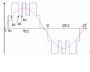
To keep the number of eliminated harmonics at a constant level, all switching angles must satisfy the condition otherwise the total harmonic distortion (THD) increases dramatically. In order to achieve a wide range of modulation indexes with minimized THD for the synthesized waveforms, a virtual stage PWM is used. The output waveform is shown in the figure.
Output waveform of virtual stage PWM control
Hence, the relation between the fundamental voltage and maximum voltage is given by modulation Index. It is given by m1, which is the ratio of fundamental voltage v1 to the maximum voltage. The maximum voltage is given by
V1 max = 4/π s Vdc
m = πv1/4s Vdc
For an 7- level inverter, there are 4 H-bridges per phase so, s=4 that is five degrees are available; one degree is used to control the magnitude of fundamental voltage and remaining degrees are used to eliminate 5th, 7th, 11th, and 13th order harmonic components.
The above statements are given by
Cos( cos(
cos( + ………. + cos(
 = 4 m1
Cos(5  + cos(5
 ……… + cos(5
 = 0
= 0
Cos(7 cos (7
 + …………….+ cos(7
The above equation is a transcendal equations known as Selective Harmonic Elimination. Here  ,
, , ,
, , , are the unknown values.
Matrix Converter
One of the most interesting families of converters is also called as matrix converter. The matrix converter is an array of bidirectional switches functioning as the main power elements. It interconnects directly the 3-phase power supply to a 3-phase load without using any DC link or large energy storage elements, and therefore it is called the all-silicon solution. The most important characteristics of the matrix converter are
- Simple and compact power circuit
- Generation of load voltage with arbitrary amplitude and frequency.
- Sinusoidal input and output currents
- Operation with unity power factor.
- Regeneration capability.
These highly attractive characteristics are the reason for the present tremendous interest in this topology. Below shown is a power circuit of the converter as a matrix of bidirectional power switches and they introduce the name matrix converter.
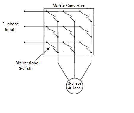
Fig. Matrix converter
One of the main advantages is the low frequency of the converter introducing the low frequency modulation index concept. In their modulation method also known as the direct transfer approach, the output voltages are obtained by the multiplication of the modulation matrix with the input voltages.
The types of multilevel inverters are explained below.
Neutral Point Clamped Converter
The neutral point clamped converter [NPC] is shown below.
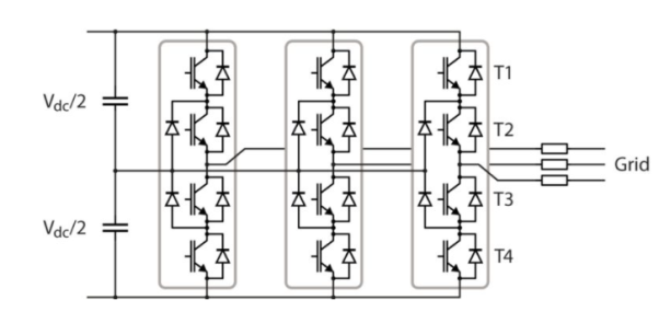
Fig. NPC converter
Each inverter consists of four transistors and they all can be controlled by 16 (=24) states. Out of these only 3 states can be used because other create short circuit on the DC link. The three states which are possible are Vdc/2, -Vdc/2 and 0V. The conductivity of transistor is shown below in the table.
T1 | T2 | T3 | T4 | Output voltage | Leg state |
ON | ON | OFF | OFF |  | P |
OFF | ON | ON | OFF | 0V | 0 |
OFF | OFF | ON | ON |  | N |
There are some modulation techniques used in NPC converter such as Carrier based PWM and space vector modulation (SV-PWM). More care is required in these inverters while balancing the voltage of the DC mid-point which cannot be achieved neutrally.
Flying Capacitor Converter
In this technique mainly capacitors are used in series and then clamped. The limited amount of voltage is transfer to electrical devices through these capacitors. There is no need of clamping diode in this type of multilevel inverters. The output voltage obtained is half of the input DC voltage. This is the main drawback of multilevel inverter. In order to balance the flying capacitor, it has switching redundancy within the phase. To control both active and reactive power they can be used. There are switching losses because of high switching frequencies.
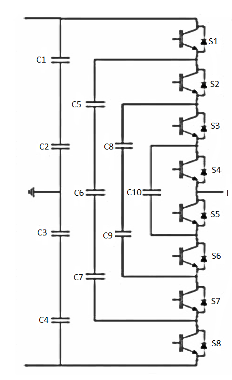
Fig. Flying capacitor multilevel inverter
They are used in IM control using direct torque control circuit. They are also used in static var generation. They also act as sinusoidal current rectifiers. We can perform both AC-DC and DC-AC conversion using these inverters.
Cascaded multilevel converter
These multilevel inverters use capacitors and switches and require a smaller number of components in each level. They consist of power conversion cells all in series and here the power can be easily scaled. The combination of capacitors and switches pairs is called as H-bridge. There is separate input DC voltage for each cell. The cells provide three level voltages of zero, positive DC and negative DC voltage levels. These converters require a smaller number of components required than those in above two types of inverters. The use of cascade multilevel inverter eliminates the use of bulky transformer required in conventional multi-phase inverters.
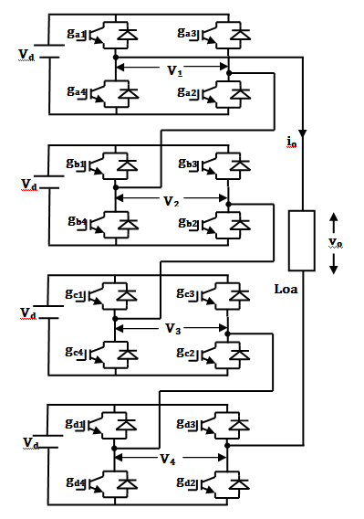
Fig. Cascade Multilevel Inverter
They are used in motor drives, active filters, electric vehicle drives, DC power source utilization, power factor compensators etc.
Comparison
S.No | Topology | Diode Clamped | Flying Capacitor | Cascaded |
1 | Power semi conductor switches | 2(m-1) | 2(m-1) | 2(m-1) |
2 | Clamping diodes per phase | (m-1)(m-2) | 0 | 0 |
3 | DC bus capacitors | (m-1) | (m-1) | (m-1)/2 |
4 | Balancing capacitors per phase | 0 | (m-1)(m-2)/2 | 0 |
5 | Voltage unbalancing | Average | High | Very small |
6 | Applications | Motor drive system, STATCOM | Motor drive system, STATCOM | Motor drive system, PV, fuel cells, battery system |
Solved Example
Q1) The separately excited dc motor in the figure below has a rated armature current of 20 A and a rated armature voltage of 150 V. An ideal chopper switching at 5 kHz is used to control the armature voltage. If La = 0.1 mH, Ra 1 , neglecting armature reaction, the duty ratio of the chopper to obtain 50% of the rated torque at the rated speed and the rated field current is?
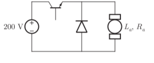
A1) Given the rated armature current

As rated armature voltage

Also for the armature, we have

And 
So we get


At the rated conditions,


For given torque

Therefore chopper output=140 V
Chopper output=140


Q2) The Voltage Source Inverter (VSI) shown in the figure below is switched to provide a 50 Hz, square wave ac output voltage Vo across an RL load. Reference polarity of Vo and reference direction of the output current io are indicated in the figure. It is given that R = 3 ohms, L = 9.55 mH.
(i) In the interval when V0 < 0 and i0 > 0 the pair of devices which conducts the load current is?
(ii) Appropriate transition i.e., Zero Voltage Switching ZVS /Zero Current Switching ZCS of the IGBTs during turn-on/turn-off is?
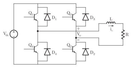
A2) (i) We consider the following two cases: Case I : When Q Q1 2 , ON In this case the +ve terminal of V0 will be at higher voltage. i.e. V0 > 0 and so i0 > 0 (i.e., it will be +ve). Now, when the Q1, Q2 goes to OFF condition we consider the second case. Case II : When Q3, Q4 ON and Q, Q2 OFF : In this condition, -ve terminal of applied voltage V0 will be at higher potential i.e., V0 < 0 and since, inductor opposes the change in current so, although the polarity of voltage V0 is inversed, current remains same in inductor i.e. I0 > 0. This is the condition when conduction have been asked. In this condition (V0 > 0, I0>0), since, IGBT’s can’t conduct reverse currents therefore current will flow through D4 D3, until ID becomes negative. Thus, D3 and D4 conducts.
(ii) When Q4 Q3, is switched ON, initially due to the reverse current it remains in OFF state and current passes through diode. In this condition the voltage across Q3 and Q4 are zero as diodes conduct. Hence, it shows zero voltage switching during turn-ON.
Q3) In the 3-phase inverter circuit shown, the load is balanced and the gating scheme is 180c conduction mode. All the switching devices are ideal. (i) The rms value of load phase voltage is? (ii) If the dc bus voltage Vd = 300V the power consumed by 3-phase load is?
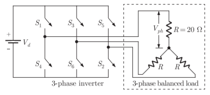
A3) For a three-phase bridge inverter, rms value of output line voltage is


(ii) 
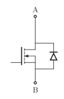
Q4) A three phase current source inverter used for the speed control of an induction motor is to be realized using MOSFET switches as shown below. Switches S1 to S6 are identical switches. The proper configuration for realizing switches S1 to S6 is?
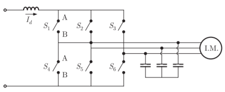
A4) The below figure allows bi direction power flow from source to the drive
Q5) The Current Source Inverter shown in figure is operated by alternately turning on thyristor pairs (T1 ,T2 ) and (T3 T4). If the load is purely resistive, the theoretical maximum output frequency obtainable will be?
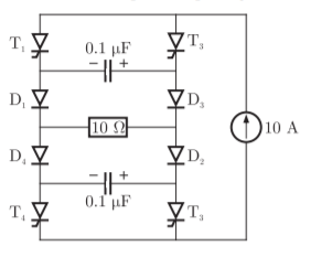
A5) In CSI let T3 and T4 already conducting at t = 0 At triggering T1 and T2, T3 and T4 are force cumulated. Again, at t= T/2, T1 and T2 are force cumulated. This completes a cycle.

Time constant =RC=4×0.5=2 sec
Frequency f
Q6) A single phase source inverter is feeding a purely inductive load as shown in the figure. The inverter is operated at 50 Hz in 180c square wave mode. Assume that the load current does not have any dc component. The peak value of the inductor current i0 will be?
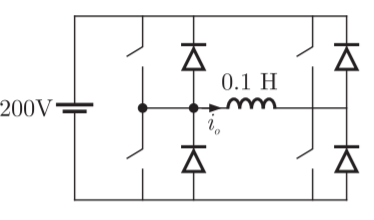
A6) Input is given as

Here load current does not have any dc component
Peak current occur at (π/)


Q7) A three phase fully controlled bridge converter is feeding a load drawing a constant and ripple free load current of 10 A at a firing angle of 30c. The approximate Total harmonic Distortion (%THD) and the rms value of fundamental component of input current will respectively be?
A7) Total rms current 
Fundamental current 


Q8) A three-phase, fully controlled thyristor bridge converter is used as line commutated inverter to feed 50 kW power 420 V dc to a three-phase, 415 V(line), 50 Hz ac mains. Consider dc link current to be constant. The rms current of the thyristor is?
A8) Given that


 =119.05
RMS value of thyristor current
Q9) A three-phase, 440 V, 50 Hz ac mains fed thyristor bridge is feeding a 440 V dc, 15 kW, 1500 rpm separately excited dc motor with a ripple free continuos current in the dc link under all operating conditions, Neglecting the losses, the power factor of the ac mains at half the rated speed is?
A9) When losses are neglected

Here back emf with  is constant


At this firing angle


Q10) The triggering circuit of a thyristor is shown in figure. The thyristor requires a gate current of 10 mA, for guaranteed turn-on. The value of R required for the thyristor to turn on reliably under all conditions of Vb variation is?
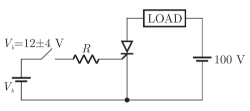
A10)


Required value of R
Q11) The circuit in figure shows a full-wave rectifier. The input voltage is 230 V (rms) single-phase ac. The peak reverse voltage across the diodes D1 and D2 is
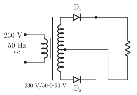
A11) Peak Inverse Voltage (PIV) across full wave rectifier is 2


Q12) An ac induction motor is used for a speed control application. It is driven from an inverter with a constant V f / control. The motor name-plate details are as follows (no. Of poles = 2) VVf N :415 :3 :50 :2850 V V Hz rpm Ph The motor runs with the inverter output frequency set at 40 Hz, and with half the rated slip. The running speed of the motor is?
A12)


Where by (V/f) control

 = new running speed of motor

Q13) The circuit in figure shows a 3-phase half-wave rectifier. The source is a symmetrical, 3-phase four-wire system. The line-to-line voltage of the source is 100 V. The supply frequency is 400 Hz. The ripple frequency at the output is
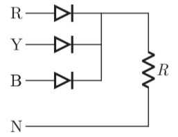
A13)
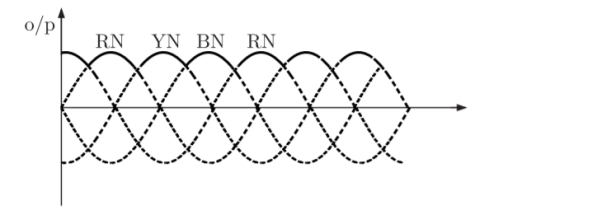
Ripple frequency 
So from  ripple frequency =1200 Hz
Q14) An inverter has a periodic output voltage with the output wave form as shown in figure

When the conduction angle, a = 1200, the rms fundamental component of the output voltage is?
A14)
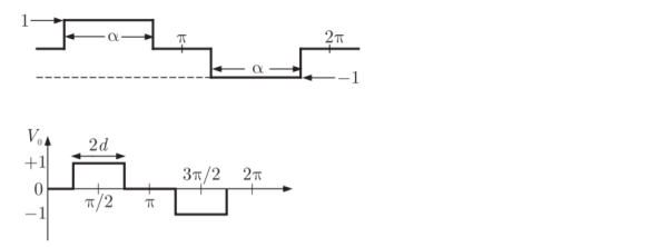
Output voltage 
RMS value of fundamental component


Q15) A variable speed drive rated for 1500 rpm, 40 Nm is reversing under no load. Figure shows the reversing torque and the speed during the transient. The moment of inertia of the drive is
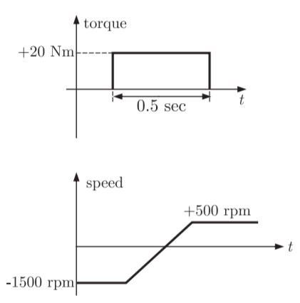
A15)


References:
- Power Electronics by Muhammad H Rashid
- Power Electronics by Evolution, Technology and applications by A.K.Bose