Unit - 4
DC to DC converters
Based on the quadrant of operation chopper can be classified as below:
Class A Chopper
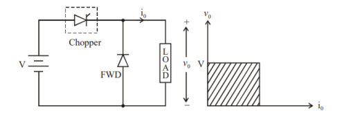
Figure 1 (a) Class A chopper
Figure shows a Class A Chopper circuit with inductive load and free-wheeling diode. When chopper is ON, supply voltage V is connected across the load that is current i0 flows as shown in figure.
When chopper is OFF, v0 = 0 and the load current continues to flow in the same direction through the free -wheeling diode. Therefore, the average values of output voltage and current are always positive. Hence, Class A Chopper is a first quadrant chopper (or single quadrant chopper).
Figure (b) shows output voltage and current waveforms for a continuous load current.
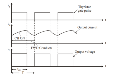
Figure 1 (b) Output voltage and current waveforms.
Class A Chopper is a step-down chopper in which power always flows from source to load. It is used to control the speed of dc motor. The output current equations obtained in step down chopper with R-L load can be used to study the performance of Class A Chopper.
Class B Chopper
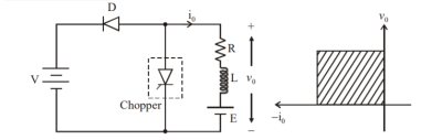
Figure 2 Class B chopper
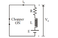
Fig. Shows a Class B Chopper circuit. When chopper is ON, and E drives a current through L and R in a direction opposite to that shown in figure. During the ON period of the chopper, the inductance L stores energy.
When Chopper is OFF, diode D conducts, and part of the energy stored in inductor L is returned to the supply. Also, the current continues to flow from the load to source. Hence the average output voltage is positive and average output current is negative.
Therefore, Class B Chopper operates in second quadrant. In this chopper, power flows from load to source. Class B Chopper is used for regenerative braking of dc motor.
Figure (b) shows the output voltage and current waveforms of a Class B Chopper. The output current equations can be obtained as follows. During the interval diode ‘D’ conducts (chopper is off) voltage equation is given by
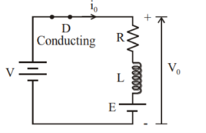

For the initial condition i.e., at. The solution of the above equation is obtained along similar lines as in step-down chopper with R-L load
Therefore 


During the interval chopper is ON voltage equation is given by

Redefining the time origin, at 
The solution for the stated initial condition is

At 
Therefore 
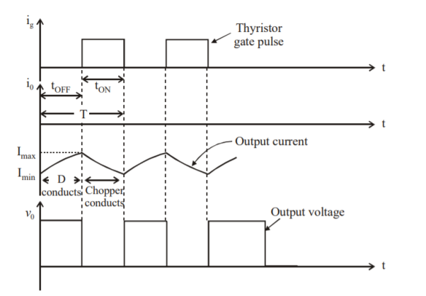
Figure 3. Class B Chopper Output Voltage and current waveform.
CLASS C CHOPPER
Class C Chopper is a combination of Class A and Class B Choppers. Figure a) shows a Class C two quadrant Chopper circuit.
For first quadrant operation, is ON or conducts and for second quadrant operation, is ON or conducts. When is ON, the load current is positive. i.e., flows in the direction as shown in figure
The output voltage is equal to  and the load receives power from the source.
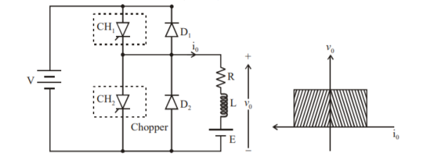
Figure 4. Class C chopper
When CH1 is turned OFF, the energy stored in inductance L forces current to flow through the diode and the output voltage vo=0V, but io continues to flow in positive direction. When CH2 is triggered, the voltage E forces io to flow in opposite direction through L and CH2. The output voltage v0=0.
On turning OFF CH2 the energy stored in the inductance drives current through diode D1 and the supply.
The output voltage v0=V the input current becomes negative and power flows from load to source.
Thus, the average output voltage vo is positive but the average output current io can take both positive and negative values. Choppers CH1 and CH2 should not be turned ON simultaneously as it would result in short circuiting the supply.
Class C Chopper can be used both for dc motor control and regenerative braking of dc motor. Figure shows the output voltage and current waveforms.
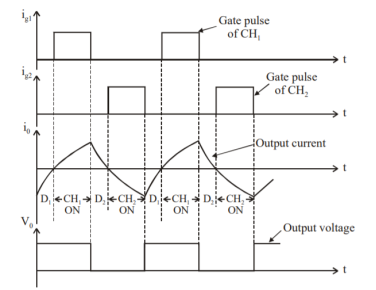
Figure 5. Class C chopper output voltage and current waveform.
Class D chopper
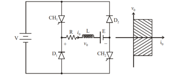
Figure 6. D chopper
Figure shows a class D two quadrant chopper circuit. When both and are triggered simultaneously, the output voltage vo=V and output current Io flows through the load in the direction shown in figure.
When CH1 and CH2 are turned off the load io continues to flow in the same direction through load.
D1 and D2 due to energy stored in inductor L but output voltage vo = -V. The average load voltage vo is positive if chopper ON time (t ON) is more than OFF time t(OFF) and the average output voltage becomes negative if ton<toFF.
Hence, the direction of load current is always positive But load voltage can be positive or negative.
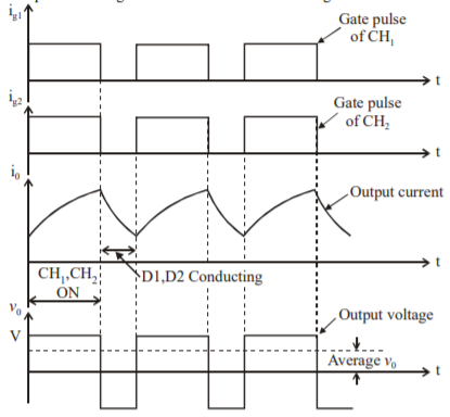
Output voltage for ton>toff
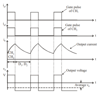
Output voltage for ton<toff
Figure 7. Output waveforms.
Class E chopper:
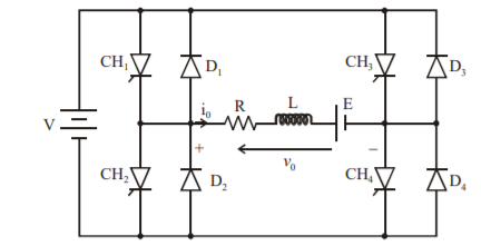
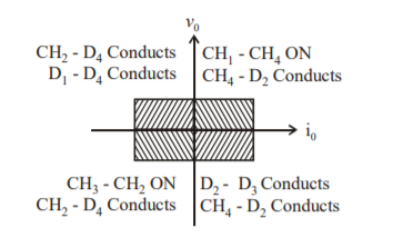
Four Quadrant Operation
Figure 8. Class E chopper
Figure shows a class E 4 quadrant chopper circuit. When they are triggered, output current flows in positive direction as shown in figure through and , with output voltage vo=V. This gives the first quadrant operation.
When both and are OFF, the energy stored in the inductor L drives through and in the same direction, but output voltage vo=-V. Therefore, the chopper operates in the fourth quadrant.
For fourth quadrant operation the direction of battery must be reversed. When Ch2 and Ch3 are triggered, the load current io flows in opposite direction and output voltage vo = -V. Since both io and vo are negative, the chopper operates in third quadrant.
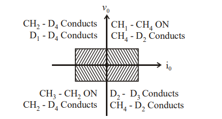
When both CH2 and CH3 are OFF, the load current io continues to flow in the same direction through D1 and D4 and the output voltage vo=V. Therefore, the chopper operates in second quadrant as vo is positive but io is negative. Figure shows the devices which are operative in different quadrants.
Key takeaway
- Class A Chopper is a step-down chopper in which power always flows from source to load. It is used to control the speed of dc motor.
- Therefore, Class B Chopper operates in second quadrant. In this chopper, power flows from load to source. Class B Chopper is used for regenerative braking of dc motor.
- Class C Chopper can be used both for dc motor control and regenerative braking of dc motor. It is the combination of class A and class B chopper.
- Class D chopper can operate in different quadrants.
Step Down Chopper with R-L load
- The figure(a) shows a step-down chopper with R-L load and freewheeling diode.
- When chopper is ON, the supply gets connected across the load and current flows from the supply to the load.
- When chopper is OFF, the load current continues to flow in the same direction through the free-wheeling diode due to the energy stored in the inductor L.
- The load current can be continuous or discontinuous depending on the values of L and duty cycle, d.
- For a continuous current operation, the load current is assumed to vary between two limits and figure (b) shows the output current and output voltage waveforms for a continuous current and discontinuous current operation.
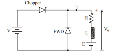
Fig 9 Step Down Chopper with R-L Load
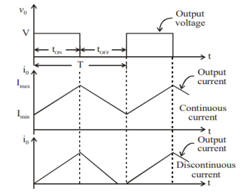
Fig 10 Output Voltage and Load Current Waveforms
When the current exceeds Imax, the chopper is turned-off and turned-on when current reduces to Imin.
Expression for Load Current for Continuous Current Operation when chopper is ON
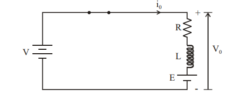
Voltage equation for the circuit as shown in figure is
V = ioR + L di0/dt + E ----------------------------------(1)
Taking Laplace Transform
V/S = R Io(s) + L [ s Io(s) – io(0-) ]+ E/s ---------------------------(2)
At t=0, initial current io(0-) = Imin
Io(s) = V-E/LS(S+R/L) + Imin / S+R/L -----------------------------------(3)
Taking Inverse Laplace Transform
Io(t) = V – E /R [ 1 – e –(R/L)t] + I min e –(R/L)t -----------------------------------(4)
This expression is valid for 0≤t≤tON during the period the chopper is ON.
At the instant the chopper is turned off load current is
Io(tON) = Imax
When chopper is OFF (0≤t≤tOFF)
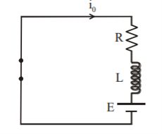
Taking Laplace Transform
0 = R Io(s) + L [SIo(s) – io(0-) + E/S]---------------------------------------------(5)
Redefining time origin we have at t=0 , initial current io(0-) = I max
Therefore Io(s) = Imax/ S + R/L - E/ LS(S+R/L)
Taking Inverse Laplace Transform
Io(t) = Imax e –R/L t – E/R[ 1 – e – R/L t ] -------------------------------------(6)
The expression is valid for 0≤t≤t OFF that is during the period chopper is OFF. At the instant the chopper is turned ON or at the end of the off period , the load current is
Io(tOFF) = I min
To find Imax and Imin
Form equation 4 at t=tON dT, io(t) = Imax
Therefore I max = V-E/R [ 1 – e – dRT/L ] + I min e –dRT/L ---------------------(7)
From equation(6) ,
At t = tOFF = T – t ON , io(t) = Imin
t = = tOFF = (1-d)T
Therefore Imin = Imax e –(1-d)RT/L – E/R[ 1 – e -(1-d)RT/L ] --------------------------(8)
Substituting Imin in equation (7) we get
I max = V/R [1 – e -(1-d)RT/L ] /[[ 1 – e – R/L t ] – E/R --------------------------------(9)
Substituting for Imax in eq(8) we get ,
I min = V/R[ e dRT/L -1]/[e Rt/L - 1] – E/R ------------------------------------------(10)
Imax-Imin is known as steady state ripple.
Therefore peak to peak ripple current  I = Imax - Imin
Average output voltage Vdc = d.V --------------------------------------------(11)
Average output current I dc = Imax + Imin /2 ------------------------------------(12)
Assuming load current varies linearly from Imin to Imax instantaneous load current is given by
Io = Imin +  I) . t/ dT for 0≤tON (dT)
Io = Imin + (Imax – Imin/dT) t ----------------------------------------(13)
RMS value of load current
Io(rms) = [1/dT  2 dt ] 1/2
Io(rms) = [1/dT  [ Imin + (Imax – Imin) t/dT ] 2 dt} ½
Io(rms) = i/dT  I 2 min + (I max – Imin/dT)2 t 2 + 2 Imin(Imax-Imin)t/dT ] dt } ½
RMS value of output current
Io(rms) = {[ I 2 min + (Imax – Imin ) 2 / 3 + Imin(Imax – Imin) ] } ½ ---------------------------(14)
RMS chopper current
I CH = [ 1/T  2 dt ]1/2
ICH = [ 1/T  I min + (Imax –Imin /dT) t] 2 } ½
ICH = ( d) ½ [ I 2 min + (Imax – Imin) 2 /3 + Imin (Imax – Imin) ] ½
ICH = ( d) ½ Io (RMS)-------------------------------------------(15)
Effective input resistance is
Ri = V /Is
Is = average source current
Is = d Idc
Therefore Ri = V/dIdc ----------------------------------(16)
Problem:
An 80 V battery supplies RL load through a DC chopper. The load has a freewheeling diode across it is composed of 0.4 H in series with 5Ω resistor. Load current, due to improper selection of frequency of chopping, varies widely between 9A and 10.2. Find
(a)The average load voltage, current and the duty cycle of the chopper.
(b) What is the operating frequency f?
(c) Find the ripple current to maximum current ratio.
Solution: (a) The average load voltage and current are:
Vav = Vo =  Vd
Vd
Iav = ½ (I2 + I1) = 9 + 10.2 / 2 = 9.6 A
Iav = Vav /R =  Vd/R
Vd/R
 = Iav . R / Vi = 9.6 x 5 / 80 = 0.6
Vav = 0.6 x 80 = 48 V
(b) To find the operating chopping frequency :
During the ON period
Vd = Ri + L di/dt…………………………………(1)
Assuming di/dt =constant
Di/dt =  / ton = 10.2 – 9 /
  T
T
L di/dt  Vd – Iav R = 80 – 5 x 9.6 = 32 V
Or
Di/dt = 32/L = 32/0.4 = 80 A.s
But di/dt = 1.2 / T = 80 = 1.2 / 0.6 T
T = 1.2 / 0.6 x 80 = 25ms
F = 1/T = 1/ 25 x 10 -3 = 40Hz
The maximum current Im occurs at 
Im =  = 1 x 80 / 5 = 16A
Ripple current Ir =  I = 10.2 – 9 = 1.2 A
Therefore Ir/Im = 1.2 / 16 = 0.075 or 7.5 %
Q) A DC Buck converter operates at frequency of 1 kHz from 100V DC source supplying a 10 Ω resistive load. The inductive component of the load is 50mH.For output average voltage of 50V volts, find: (a) The duty cycle (b) ton (c) The rms value of the output current (d) The average value of the output current (e) Imax and Imin (f) The input power (g) The peak-to-peak ripple current.
Solution:
a) Vav = Vo = =  Vd
Vd
 = Vav / Vd = 50/100 = 0.5
b) T = 1/f = 1/1000 = 1ms
 = ton/T
 =
=  T = 05 x 1ms = 0.5 ms
c) Vo (rms) = ( Vi = (0.5) ½ x 100 = 70.7 V
d) Iav = Vav / R = 50/10 = 5A
e) Imax = Vav/R + toff/2L Vav = 50/10 + (1-0.5) x 10 -3 / 2 x 50 x 10 -3 x 50
= 5 – 0.25 = 4.75A
f) Is(av) =  / 2 (Imin + Imax) =
  = 0.5 x 5 = 2.5 A
Pin = Is(av) Vd = 2.5 X 100 = 250 W
g) Ip-p =  I = Imax - Imin = 5.25 – 4.75 = 0.5 A
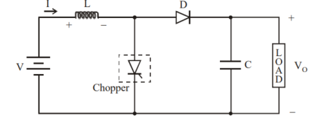
Figure 11 Step Up chopper
The figure shows Step Up chopper. To obtain load voltage Vo higher than the input voltage V. The values of L and C are chosen depending on the requirement of output voltage.
When the chopper is ON the inductor L is connected across the supply. The inductor current I rises and stores energy during ON time of the chopper tON.
When the chopper is off the inductor current is forced to flow through the diode D and load for a period t OFF. The current tends to decrease resulting in reversing the polarity of induced EMF in L. Therefore, voltage across load is given by

If a large capacitor ‘C’ is connected across the load, then the capacitor will provide a continuous output voltage. Diode D prevents any current flow from capacitor to the source. Step up choppers are used for regenerative braking of dc motors.
Expression for Output Voltage:
Assume the average inductor current to be I during ON and OFF time of Chopper.
When Chopper is ON
Voltage across inductor L=V
Therefore, energy stored in inductor = V.I.ton.
TOn = On period of chopper.
When Chopper is OFF (energy is supplied by inductor to load)
Voltage across L = V0 – V
Energy supplied by inductor L = (Vo-V) I t OFF
Where t OFF = OFF period of chopper.
Neglecting losses, energy stored in inductor L = energy supplied by inductor L
Therefore 


Where
T=Chopping period or period of switching


Where  duty cycle
For variation of duty cycle ‘d’ in the range 0<d<1 the output voltage Vo will vary in the range V<Vo<∞.
Control Strategies:
A chopper is used to step up or step down the fixed DC i/p voltage. The chopper system gives high efficiency, smooth control, regeneration and fast response.
There are two kinds of control strategies used in DC choppers
- Time ratio control
- Current limit control.
Time Ratio Control
In the time ratio control the value of the duty ratio, K =TON /T is changed. Here ‘K’ is called the duty cycle. There are two ways to achieve the time ratio control, namely variable frequency and constant frequency operation.
Constant Frequency Operation
In constant frequency control strategy operation, the ON time TON is changed, keeping the frequency, f=1/T, or time period ‘T’ constant. This operation is also called PWM (pulse width modulation control) .Hence; the output voltage can be varied by varying ON time.
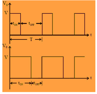
Fig 12 Constant Frequency Operation
Variable Frequency Operation
In variable frequency control strategy operation, the frequency (f = 1/T) is changed, then the time period ‘T’ is also changed. This is called as frequency modulation control.
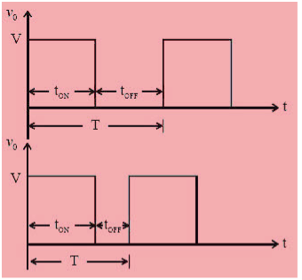
In both cases, the o/p voltage may be changed with the change in duty ratio.
Current Limit Control
In DC-to-DC converter, the current value varies between the maximum as well as the minimum level of constant voltage. In this method, the DC-to-DC converter is turned ON & then OFF to confirm that current is preserved constantly between the upper limits and lower limits. When the current energies go beyond the extreme point, the DC-DC converter goes OFF.
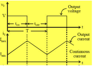
Fig 13 Current Limit Control
- When the switch is in its OFF state, current freewheels through the diode and falls in an exponential manner.
- The chopper is turned ON when the flow of current spreads the minimum level. This technique can be utilized either when the ON time ‘T’ is endless or when the frequency f=1/T.
Class C Chopper is a combination of Class A and Class B Choppers. Figure shows a Class C two-quadrant Chopper circuit. For the first quadrant operation, CH1 is ON or D2 conducts and for second quadrant, operation CH2 is ON or D1 conducts. When CH1 is ON, the load current i0 is positive that is io flows in the direction as shown in figure.
The output voltage is equal to V(vo=V) and the load receives power from the source.
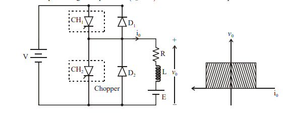
When CH1 is turned OFF, energy stored in inductance L forces current to flow through the diode D2 and the output voltage v0=0,but io continues to flow in positive direction.
When CH2 is triggered the voltage E forces io to flow in opposite direction through L and CH2.. The output voltage v0=0. On truning OFF CH2 the energy stored in the inductance drives current through diode D1 and the supply; output voltage v0=V the input current becomes negative and power flows from load to source.
Thus the average output voltage vo is positive but the average output current io can take both positive and negative values. Choppers CH1 and CH2 should not be turned ON simultaneously because it results in short circuit .
Class C Chopper can be used for both dc motor control and regenerative braking of dc motor.
The figure shows the output voltage and current waveforms.
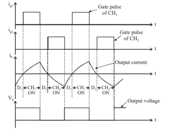
Fig 14. Class C chopper output waveforms
Class E Chopper
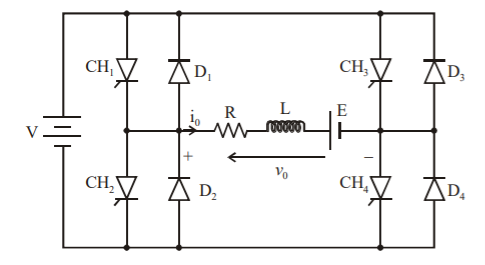
Fig 15. Class E Chopper
Four Quadrant Operation
- The figure shows a class E 4 quadrant chopper circuit . When CH1 and CH4 are triggered the output current i0 flows in positive directionas shown in figure through CH1 and CH4 with output voltage v0 + V. This gives the first quadrant operation.
- When both CH1 and CH4 are OFF the enrgy stored in the inductor L drives io through D and D2 in the same direction, but the outpur voltage vo = -V.
- Therefore the chopper operates in the fourth quadrant. For fourth quadrant opertion the direction of the battery must be reveresed.
- When CH2 and CH3 are triggered the load current i0 flows in opposite direction and the output voltage v0=-V.
- Since both io and vo are negative the chopper operates in the third quadrant. When both CH2 and CH3 are OFF the load current io continues to flow in the same direction through D1 and D4 and the output voltage vo=V.
- Therefore the chopper operates in second quadrant as vo is positive but i0 is negative.
SMPS:(Flyback/Half Bridge/ LM3524 based or equivalent circuit)
A Power Supply Unit is an important part of an electric circuit as it provides the power to the circuit for a proper operation. Almost all electronic devices require a constant voltage without any fluctuations.
A power supply will take an unregulated power and converts it into a stable regulated power. There are two categories of Power Supplies: Linear Regulated Power Supply and Switching Mode Power Supply (SMPS).
Linear Regulated Power Supply is a type of power supply that regulates the output voltage with the help of a series pass control element. The basic example of a series pass element is a resistor.
Depending on the changes in either input or load, the current through the transistor changes in order to keep the output constant.
The difference between the input and output (load) voltages is dropped across the transistor and this excess power that is the difference between the input and output (load) power is dissipated as heat by the transistor.

Fig 16 Linear Regulated Power Supply
The input AC source is given to a rectifier and filter to convert it into DC. But this DC Supply is unregulated as it is susceptible to change with the changes in input. This unregulated DC supply is given as input to the Linear Regulator.
SMPS is a type of regulated power supply that uses a high frequency switching regulator to convert the power supply and also regulate the output in a highly efficient way.
The switching regulator is again a transistor (like a power MOSFET) just like in Linear Regulator but the difference is that the pass transistor in SMPS doesn’t continuously stay in saturation or fully ON state but rather switches between fully ON and fully OFF states at a very high frequency. Hence the name Switching Mode Power Supply.
Since the average time the switching element that is the transistor stays in active state is less, the amount of power wasted or dissipated as heat is very less when compared to Linear Regulators.
This in turn leads to high efficiency of SMPS as the voltage drop across the pass transistor (or switching element) is very less.
The switching action of the transistor is controlled using a technique called Pulse Width Modulation (PWM) and the output voltage can be regulated by the duty cycle of the PWM.
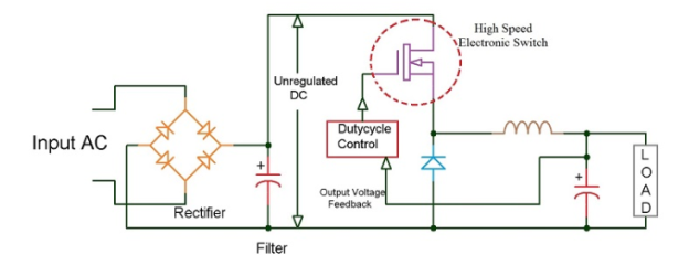
The figure shows a basic structure of an SMPS unit. In this, the unregulated DC supply is given to a Switched Mode DC – to – DC Chopper Circuit and the output is a regulated DC Supply.
The main difference between the structures of Linear Regulated Power supply and Switch Mode Power Supply shown here is that in case of Linear Power Supply, the input AC is stepped down, rectified and filtered to get unregulated DC and in case of SMPS, the input AC is directly rectified and filtered and the unregulated high voltage DC is given to a High Frequency DC – to – DC Converter.
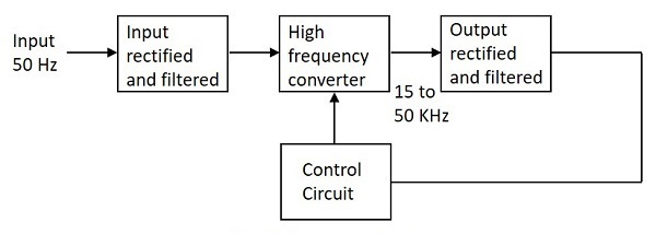
The Switched mode power supply is abbreviated as SMPS is used to convert the regulated DC output voltage from unregulated DC or AC voltage. The basic block diagram showing the working of SMPS is represented below.
Input Unit
The rectifiers and the filters are fed with a 50Hz input supply. The capacitance value of the capacitor should be high as there can be fluctuations in the output. There is no need for any transformer for input supply as the rectifier and filter circuit combinations are used.
Switching Section
As there are various fluctuations at the output of the input unit Power transistors or MOSFETs are used for fast switching. They can be turned ON or OFF as per the need and the output from here is fed to the transformer present in this section.
Output Unit
The desired DC output is obtained by again passing the output from the switching section to the rectifier and filter unit. The regulated output voltage obtained from here is again fed as input to the control unit through a feedback circuit.
Control Unit
The control unit consists of many other small units functioning together as represented below.

The input to the control unit is fed to the sensor. The final output voltage is controlled by controlling the chopping frequency. This helps to maintain the final voltage level. This is achieved by comparing the error amplifier inputs. The input to the error amplifier is the signal from the sensor and one reference signal. The reference signal is nothing but the required output signal; the error amplifier compares the mentioned two signals and generates the required output voltage level accordingly. The PWM oscillator produces a standard PWM wave fixed frequency.
Types of SMPS
There are four main types of SMPS listed below
- DC to DC Converter
- AC to DC Converter
- Fly back Converter
- Forward Converter
Applications
There are many applications of SMPS. They are used in the motherboard of computers, mobile phone chargers, HVDC measurements, battery chargers, central power distribution, motor vehicles, consumer electronics, laptops, security systems, space stations, etc.
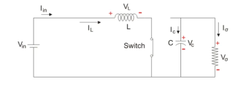
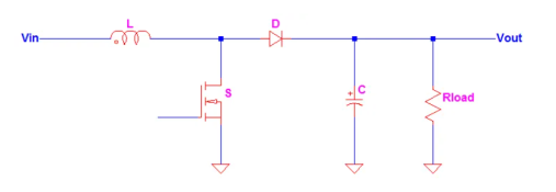
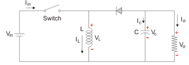
A typical Boost converter is shown below.
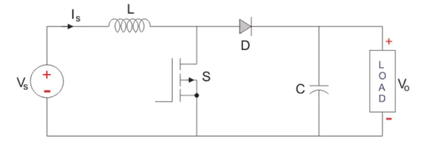
The input voltage source is connected to an inductor. The solid-state device which operates as a switch is connected across the source. The second switch used is a diode. The diode is connected to a capacitor, and the load and the two are connected in parallel as shown in the figure above.
The inductor connected to input source leads to a constant input current, and thus the Boost converter is seen as the constant current input source. And the load can be seen as a constant voltage source.
The controlled switch is turned on and off by using Pulse Width Modulation (PWM).
The Boost converter has two modes of operation. The first mode is when the switch is on and conducting.
Mode I: Switch is ON, Diode is OFF
The switch is ON and therefore represents a short circuit ideally offering zero resistance to the flow of current so when the switch is ON all the current will flow through the switch and back to the DC input source. Let us say the switch is on for a time TON and is off for a time TOFF. We define the time period, T, as
T = TON + T OFF
And the switching frequency
f switching = 1/T.
Let us now define another term, the duty cycle,
D = TON/T
Let us analyze the Boost converter in steady state operation for this mode using KVL.
Vin = VL
VL = L diL /dt = Vin
DiL/dt = ∆ iL/∆t = ∆iL/DT = Vin/L
Since the switch is closed for a time Ton = DT we can say that ∆t=DT
(∆ iL) closed= (Vin/L) DT
Analysis and waveforms at steady state
Let us analyze the Boost converter in steady state operation for this mode using KVL. Since the switch is closed for a time TON = DT we can say that Δt = DT.
While performing the analysis of the Boost converter, we have to keep in mind that
- The inductor current is continuous and this is made possible by selecting an appropriate value of L.
- The inductor current in steady state rises from a value with a positive slope to a maximum value during the ON state and then drops back down to the initial value with a negative slope. Therefore, the net change of the inductor current over anyone complete cycle is zero.
Mode II: Switch is OFF, Diode is ON
In this mode, the polarity of the inductor is reversed. The energy stored in the inductor is released and is ultimately dissipated in the load resistance, and this helps to maintain the flow of current in the same direction through the load and also step-up the output voltage as the inductor is now also acting as a source in conjunction with the input source. But for analysis, we keep the original conventions to analyze the circuit using KVL.
Let us now analyse the Boost converter in steady state operation for Mode II using KVL.
Vin = VL + Vo
VL = L diL/dt = Vin -VO
DiL/dt = ∆ iL/∆t = ∆ iL / (1-D) T = Vm-Vo/L
Since the switch is open for a time
TOFF = T – TON = T -DT = (1-D) T
We can say that
∆t = (1-D) T
(∆ iL) open = (Vin -Vo/L) (1-D) T
It is already established that the net change of the inductor current over any one complete cycle is zero
(∆ iL) closed + (∆ iL) open =0
(Vin – Vo) /L (1-D) T + (-Vo/L) DT =0
Vo /Vin = 1/ 1-D
Since the switch is open for a time
TOFF = T – TON = T – DT = (1-D) T
We can say that
∆t = (1-D) T
It is already established that the net change of the inductor current over any one complete cycle is zero.
(∆ iL) closed + (∆ iL) open =0
(Vin – Vo/L) (1-D) T + (-Vo/L) DT =0
Vo /Vin = 1/ 1-D
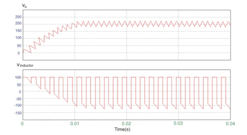
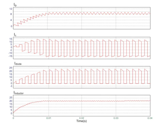
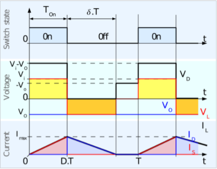
A circuit of a Boost converter and its waveforms are shown below. The inductance, L, is 20mH and the C is 100µF and the resistive load is 20Ω. The switching frequency is 1 kHz. The input voltage is 100V DC and the duty cycle is 0.5.
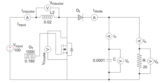
The voltage waveforms are as shown above and the current waveforms are as shown in the figure below.
The voltage waveforms are as shown above and the current waveforms are as shown in the figure below.
Relation between duty ratio and average output voltage.
The inductor of the boost converter charges during Ton and discharges during Toff. The inductor current waveform is then resembled like Figure 2 below.
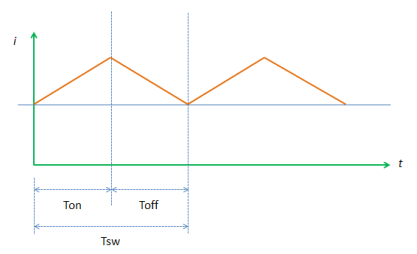
The figure is an inductor waveform of a continuous conduction mode boost converter. A boost converter by the way can operate in three modes; continuous conduction (CCM), discontinuous conduction (DCM) and boundary mode. For CCM the inductor current will not reach zero after every switching cycle. For DCM, the inductor current is reaching zero before the next Ton occur.
How to Calculate the Duty Cycle of Boost Converter – Analysis during Ton
During Ton, the switch S is on. The diode will be reversed biased and this
time the load is being supplied by the energy stored in the capacitor C. The inductor will charge. The flow of the current is from Vin to inductor L then to switch S. By KVL,

Then expressing VL
 -Vsw-------------------------(1)
The voltage across inductor is also defined by below formula.
 ---------------------------------------(2)
Expressing the change in current di
 ---------------------------------------(3)
Substitute 1 to 3
 ----------------------------------------(4)
Then we will get rid of the variable dt by integrating the equation from 0 to Ton.

 ----------------------------------------------------(5)
How to Calculate the Duty Cycle of Boost Converter – Analysis during Toff
During Toff, the inductor reverses its polarity and the diode at this time will be forward biased and the load will be supplied by the energy in the inductor. The energy on the inductor will start to decay. The flow of current is from Vin to diode D then to the load. Applying KVL,

Expressing VL,

------------------------------------------(6)
Substituting [Eq. 6] to [Eq. 3] will result to
 ----------------------------------(7)
Then we will eliminate the variable dt through integration from Ton to T.
 ---------------------------------------(8)

Now go back to Figure 2, the magnitude of the inductor current during Ton and Toff is equal. Therefore, we can equate [Eq. 5] and [Eq. 8].


Then substitute Ton = DT

Then solving for the duty cycle, D
 -----------------------------------------------------Eq. 9
Assuming ideal values (diode and switch voltage drops are zero)
 ----------------------------------------(10)
Output Voltage:
The relationship of voltage and current for an inductor is:

Or

For a constant rectangular pulse:

From this we can see that the current is a linear ramp, when the voltage is a constant pulse.
When the transistor switches on the current is:

Or

And when the transistor switches off the current is:


(Equation 1)
Where VD is the voltage drop across the diode, and VTrans is the voltage drop across the transistor. Note that the continuous/discontinuous boundary occurs when io is zero.
By equating through delta i, we can solve for Vout:


We can also solve for the duty cycle as follows,


If we neglect the voltage drops across the transistor and diode then:

So, it is clear that the output voltage is related directly to the duty cycle of the pulses.
Buck Boost Converter
It is basically a DC-DC converter which has output either low or high than the input voltage value. It is combination of a step up (Buck) and step up (Boost) converter. These devices have a diode connected with inductor and a capacitor. The input is connected to a solid-state device. The diode acts as a switch. The circuit shown below is of a buck-boost converter.

Fig 17: Buck-Boost Converter
The diode is in the reverse direction to the source. The capacitor and diode are in parallel to load. We use pulse width modulation to turn the controlled switch ON and OFF. Normally time based PWM is used as frequency based is difficult in implementation. This operates in two modes
i) When switch is ON, Diode is OFF:
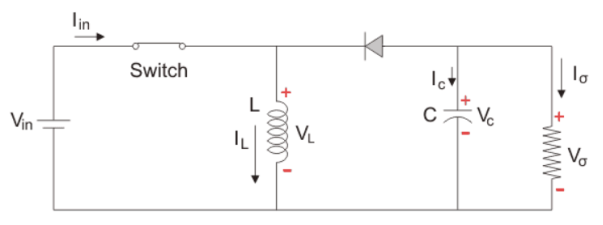
As seen from the above figure when the switch is ON it acts as a short circuit and hence, allows all the current to pass through it. In this condition the current flows through the switch and inductor and again to the input. The inductor stores energy at this time. When the switch is OFF the inductor reverses its polarity and then the current flows through the load and then diode and back to the inductor.
The total time period T = TON+TOFF
TON: ON time
TOFF: OFF time
The switching frequency fs= 1/T
In steady state Vin=VL
VL= L  = Vin
= Vin
Now duty cycle D= 
 =
= 
At end of ON state
 ILON =
  =
=  dt =
dt = 
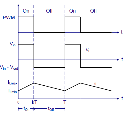
Ii) When switch is OFF, Diode is ON:
The circuit is shown below where the switch is in OFF state. The polarity of inductor is reversed. The current flows through the load resistance from the inductor and a step-up voltage is obtained at the output.
In this case VL=Vo
VL= L  = Vo
= Vo
 =
= 
TOFF= T-TON = T_DT = (1-D) T
 t= (1-D) T
 iL)open=
  (1-D) T
Solved Examples
Q1) A transistor dc chopper circuit (Buck converter) is supplied with power form an ideal battery of 100 V. The load voltage waveform consists of rectangular pulses of duration 1 ms in an overall cycle time of 2.5 ms. Calculate, for resistive load of 10 Ω. (a) The duty cycle γ. (b) The average value of the output voltage Vo. (c) The rms value of the output voltage Vorms. (d) The ripple factor RF. (e) The output dc power.
A1)
(a) 

(b) 


Q2) An 80 V battery supplies RL load through a DC chopper. The load has a freewheeling diode across it is composed of 0.4 H in series with 5Ω resistor. Load current, due to improper selection of frequency of chopping, varies widely between 9A and 10.2. (a) Find the average load voltage, current and the duty cycle of the chopper. (b) What is the operating frequency f ? (c) Find the ripple current to maximum current ratio.
A2)
(a) The average load voltage and current are

(a) The average load voltage and current are:


(b) To find the operating (chopping) frequency:
During the ON period, 
Assuming 

From eq (1)


But


Hence 
The maximum current  occurs at =1

Ripple current 

Q3) A DC Buck converter operates at frequency of 1 kHz from 100V DC source supplying a 10 Ω resistive load. The inductive component of the load is 50mH.For output average voltage of 50V volts, find: (a) The duty cycle (b) ton (c) The rms value of the output current (d) The average value of the output current (e) Imax and Imin (f) The input power (g) The peak-to-peak ripple current.
A3)
(a) 

(b) 

(c) 
(d) 
(e) 
(f)


(g)

Q4) A Chopper circuit is operating on TRC at a frequency of 2 kHz on a 460 V supply. If the load voltage is 350 volts, calculate the conduction period of the thyristor in each cycle.
A4)

Chopping period 

Output voltage 
Conduction period of thyristor


Q5) Input to the step up chopper is 200 V. The output required is 600 V. If the conducting time of thyristor is 200 ssec. Compute Chopping frequency, If the pulse width is halved for constant frequency of operation, find the new output voltage.
A5)
Vs = 220V, R = 20 Ω, f = 10KHz.
d = tON/T = 0.80
Vch = voltage drop across chopper = 1.5 Volts
Average output voltage
Vdc = (tON/T) (Vs-Vch)= 0.80(220-1.5) = 174.8Volts
Chopper ON time tON = dT
Chopping period T=1/f = 1/10 x 10 3 secs = 100 µsec
Chopper ON time
TON = dT
TOn = 0.80 x 0.1 x 10 -3 = 80 µ sec.
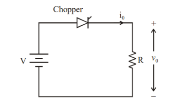
Q6) A dc chopper in figure has a resistive load of and input voltage of V = 200 V. When chopper is ON, its voltage drop is 2 V and the chopping frequency is 1 kHz. If the duty cycle is 60%, determine Average output voltage RMS value of output voltage Effective input resistance of chopper Chopper efficiency.
A6)
 Cho[[er voltage drop,
Average output voltage


RMS value of output voltage


Effective input resistance of chopper is


Output Power:


Input Power:


Chopper efficiency


Q7) A chopper feeding on RL load is shown in figure, with V = 200 V, R = 5, L = 5 mH, f = 1 kHz, d = 0.5 and E = 0 V. Calculate – Maximum and minimum values of load current. – Average value of load current. – RMS load current. – Effective input resistance as seen by source. – RMS chopper current.
A7)


Chopping period is 
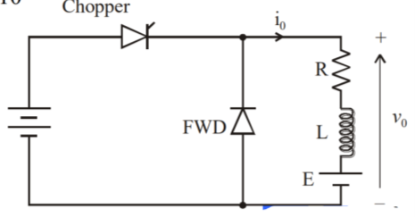
Maximum value of load current is given by


Minimum value of closing current is given by


Average value of load current is

For linear variations of current

RMS load current is given by


RMS chopper current is given by

Effective input resistance is

 Average source current


Therefore effective input resistance is

Q8) In a dc chopper, the average load current is 30 Amps, chopping frequency is 250 Hz, supply voltage is 110 volts. Calculate the ON and OFF periods of the chopper if the load resistance is 2 ohms.
A8)

Chopping period 


Chopper ON period,

Chopper OFF period,


Fly Back Converter
Figure below shows the flyback converter. It consists of a power MOSFER M1, transformer for isolation purpose, diode D and capacitor C and a load. An uncontrolled rectifier converts ac to dc output which is fed to flyback SMPS. When power MOSFET is turned on, supply voltage Vs is applied to the transformer primary v1=Vs. A corresponding voltage v2 with polarity as shown in figure is induced in the transformer secondary.
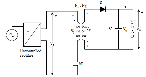
Fig 18. Flyback Converter
v2=VsN2/N1
As v2 is reverse biases diode D the new equivalent circuit will then become as shown below. Filter capacitance C is assumed large enough so that capacitor voltage vc(t) = load or output voltage V0 is taken almost constant. When M1 is turned off a voltage of positive polarity is induced in primary and secondary winding as shown below. Voltage across transformer secondary is given as
v2= -V0=-VsN2/N1
D is forward biased and starts conducting current iD. As a result energy stored in the transformer core is delivered partly to load and partly to charge the capacitor C.
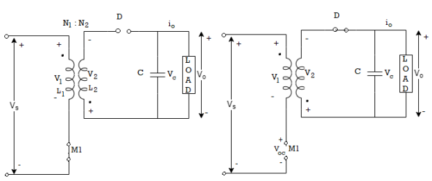
From the waveform shown below the time when M1 is on
v1=Vs
v2=VsN2/N1
For magnetizing current, it is assumed that transformer core is not demagnetized completely at the end of periodic time
T = Ton +Toff
During Ton magnetizing current rises linearly from its initial value Im0 to Im1 at t= Ton. With the rise of im during Ton magnetic energy gets stored in the transformer core.
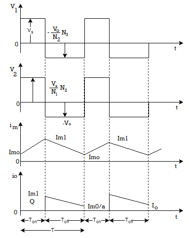
Fig 19. Waveform
im(t) = Imo+ (Vs/L) t 0<t<Ton
At t= Ton
Im (Ton) = Im0 = Imo + (Vs/L) t
When M1 is turned off, the emf induced in primary and secondary windings are reversed as shown above. Diode D is now forward biased. A current in transformer secondary winding begins to flow through D. The current im is reduced from Im1 to Imo at t =T, transformer energy is delivered to load.
During Toff, M1 is off and
v2=-V0
v1 =-VoN1/N2
The value of current im will now become
im(t) = Im- (V0N1/N2) [(t-Ton)/L]
At t= T1
im(T) = Im1- (V0N1/N2) [(T-Ton)/L]
im(T) = Im0 + (Vs Ton/L)- (V0N1/N2) [(T-Ton)/L]
The energy stored in core over periodic time T is zero
im (0) = im(T)


a=N2/N1 = Transformer Turn ratio
k=Ton/T= Duty cycle of Flyback converter


The above equation gives current on primary side of the transformer. This current when referred to secondary side, is equal to the diode current iD.


Half Bridge Converter
The circuit consists of uncontrolled rectifier two capacitors C1 and C2, two power MOSFETs M1 and M2 one transformer with mid-tap on the secondary side, two diodes D1 and D2 and filter components L and C.
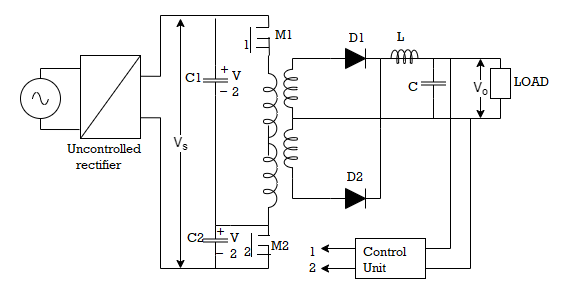
Fig 20. Circuit Diagram
The capacitors C1 and C2 have equal capacitance therefore voltage across each of the two is Vs/2. When M1 is turned on, voltage of C1 appears across transformer primary v1 = Vs/2 and voltage induced in secondary is v2= VsN2/2N1 and diode D1 geta forward biased. When M2 is turned on, a reverse voltage of Vs/2 appears across transformer primary from C2, v1 = - Vs/2 and voltage induced in the secondary winding v2= -VsN2/2N1 therefore diode D2 gets forward biased. The average output is
V0 = VsN2/2N1
When M1 is off, open circuit voltage across M1 terminals is Voc = Vs. For h.v.d.c. Applications half bridge converter is therefore preferred over push pull converters.
Full Bridge Converter
The circuit consists of an uncontrolled rectifier with four MOSFETs, transformer with mid tap secondary, two diodes and LC filter circuit. The function of control circuit is to sense the output load voltage and to decide the duty ratio of MOSFETs.
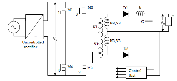
Fig 21. Circuit Diagram
When M1 and M2 are turned on together the voltage Vs appears across transformer primary v1=Vs and secondary voltage v2=VsN2/N1=a Vs. Diode D1 gets forward biased and V0=a Vs. When M3 and M4 are turned on together, the primary voltage is reversed v1=-Vs and v2=VsN2/N1=a Vs. Therefore, diode D2 now begins to conduct and the output voltage is again V0=a Vs.
The overall size of SMPS depends upon its operating frequency. Use of power transistors is limited to approximately 40 to 50 kHz. The main advantages of SMPS over conventional linear power supplies are as under:
- For the same power rating, SMPS is of smaller size, lighter in weight and possesses higher efficiency because of its high frequency operation.
- SMPS is less sensitive to input voltage variations.
The disadvantages of SMPS are as follows:
- SMPS has higher output ripple and its regulation is worse.
- SMPS is a source of both electromagnetic and radio interference due to high frequency switching.
- Control of radio frequency noise requires the use of filters on both input and output of SMPS.
The advantages possessed by SMPS far outweigh their shortcomings. This is the reason for their wide spread popularity and growth.
The main component in an SMPS that enables the efficient power conversion is the inductor or a ferrite transformer based coil, controlled or switched by PWM.
The pulse width modulation or the PWM plays an important role for switching the inductor through a power transistor with calculated duty cycle so that the inductor is able to implement the DC to DC conversion with maximum efficiency.
Since the PWM becomes the crucial factor in an SMPS, an ideal PWM generator/controller IC such as SG3524 or LM3524 becomes extremely suitable for making these types of buck and boost converter designs.
Boost Converter Using LM3524
In the above simple SG3524 boost converter design we can see the collectors of the internal driver BJTs CA and CB are joined together for enforcing the ON/OFF switching of the inductor L1 through an appropriately calculated PWM rate.
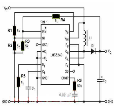
The PWM rate is set by configuring the SG3524 error amp inputs INV and NI, which is internally set as a comparator, and whose output controls the output PWM.
This feedback potential at the INV input determines the output pulse cut-off threshold, and the PWM duty cycle. This threshold limit is fixed with reference to the sample voltage set at the NI input of the error amp through the two 5 k resistors (R1, R2 shown in orange).
Calculating the Feedback Resistor
RF = 5k [(VO / 2.5) -1] = 5000 [(VO / 2.5) -1] this equation sets up the feedback resistor for the PWM control, using the parameters VO = output step-up voltage, and R3 = 5 k.
Calculating Oscillator Frequency
FOSC = 1 / RT * CT this equation sets up the frequency of the converter, which must be anywhere around 30 to 100 kHz. Higher frequencies will mean small L1 inductor.
Calculating the Inductor
L1 = 2.5VIN2 (VO - VIN) / fOSC * IO* VO2 this equation help us to determine the inductance rating for the L1 inductor, using the parameters VIN = input supply voltage, the VO = output voltage, f OSC = frequency, and the IO = output current
Calculating the Output Capacitor
CO = IO (VO - VIN) / fOSC * ΔVO * VO this equation helps us to calculate the output filter capacitor CO, using the parameters IO = output current, VO = output boosted voltage, VIN = input supply voltage, fOSC = frequency, ΔVO = peak-to-peak output ripple.
Step Up Converter
The next diagram below shows how the same concept could be upgraded to a high current DC to DC boost converter circuit using the very same SG3524 circuit, except the output stage where high power transistors are used for facilitating the required current amplification.
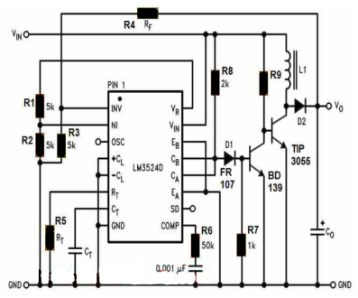
This circuit can be used for stepping up or boosting any low voltage (above 5 V) to a desired higher level, without any limitations in the current level.
R9 will depend on the output current spec of the converter, and could be calculated using the formula:
R9 = (VIN - 0.7) * hFE / Max IO
Here, VIN is the input supply voltage, hFE is the current gain of TIP3055, and IO is the maximum output current.
Step-Down Buck Converter using SG3524
The next DC to DC converter circuit using SG3524 discussed below is a step down buck converter which will allow you to convert any higher level DC voltage (below 40 V) into a desired lower DC output voltage, but with an input current not exceeding 80 mA.
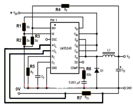
Meaning, suppose you are trying to make a 48 V inverter, in which the oscillator circuit can work only with a regulated 15 V DC. In such a situation you can effectively apply this buck converter concept for stepping down 48 V to 15 V DC for powering the oscillator circuit safely and allowing the 48 V to be used by the inverter power devices and the transformer.
In this configuration we find the IC SG3524 pinout features are configured in the following manner:
The emitters EA and EB of the ICs output transistors are joined together for driving the inductor L1, while the collectors CA and CB are joined together with the input supply Vin for supplying the current to the L1 via the emitters.
The feedback resistor RF (R4) along with the associated 5 k divider resistor R3 is configured as before with the error amplifier, while the reference to the error amp is rigged using R1, R2 via the +5 V supply from the VR (VREF) pin of the IC. This takes care of the PWM control.
High Current Step-Down Converter
In the above example we learned the low current version of the SG3524 DC step-down converter, without involving external power devices.
For higher current levels, an external power switching transistors could be added, along with other upgraded components such as the L1 inductor and diode.
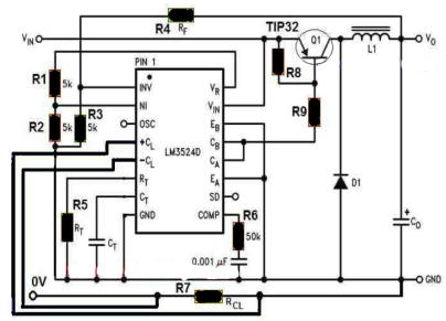
The various equations and calculations involved in this SG3524 buck converter circuit can be learned as given below:
Calculating the Feedback Resistor
RF = 5 k [(VO/2.5) - 1] 5000 [(VO/2.5) - 1], this equation is used for fixing the feedback resistor RF(R4) which controls the output PWM
Calculating the Current Sensing Resistor
RCL = Current Limit Voltage / IO(MAX), this equation is used for evaluating the current sensing resistor RCL or the R7, with respect to the maximum desired output current limit IO(MAX) .
The current limit voltage refers to the desired voltage drop that needs to be developed across RCL when IO(MAX) is reached. This current limit voltage could be anywhere between 0.3 V to 1 V, the smaller the better to ensure a smaller RCL
Calculating the Oscillator Frequency
FOSC = 1 / RT*CT this equation allows us to set up the oscillator frequency of the converter, and this can be anywhere between 30 kHz and 100 kHz. Higher frequencies will cause the L1 to be smaller and vice versa.
Calculating the Inductor
L1 = 2.5VO (VIN - VO) / IO*VIN*fOSC this equation can be used for determining the inductor L1 value which becomes the crucial element of the step down converter. In this equation, VO is the desired stepped down output voltage, VIN is the input supply voltage, IO is the maximum output current, fOSC is the oscillator frequency.
The 2.5 value is acquired from the reference voltage formed by the resistive divider using the two 5 k resistors R1, R2 at the NI input of the SG3524 IC error amp.
Calculating the Output Capacitor
CO = (VIN - VO) VO* T2 / 8 *ΔVO *VIN*L1, this equation facilitates determining the output filter capacitor CO, using the available data such as the input supply VIN, output stepped down voltage VO, output peak to peak ripple voltage ΔVO, the inductance of L1, and the period T2 where T = 1 / fOSC
A typical solar panel converts only 30 to 40 percent of the incident solar irradiation into electrical energy. Maximum power point tracking technique is used to improve the efficiency of the solar panel. According to Maximum Power Transfer theorem, the power output of a circuit is maximum when the Thevenin impedance of the circuit (source impedance) matches with the load impedance. Hence our problem of tracking the maximum power point reduces to an impedance matching problem. A simple Maximum Power Point Tracking System is shown below. A simple MPPT-PV Standalone Power System is presented which consists of an array of photovoltaic module (power source), a resistive load and a step-up switching mode DC-DC converter to act as power interface between the PV array and load.
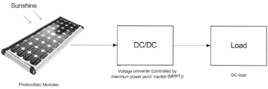
Figure 22 Block Diagram of Proposed MPPT System
One significant problem in PV power system is the probable match between the operating characteristics of the load and the PV array. Maximum Power Point tracking is specifically designed to remove the mismatch. Shown in Figure 3 is a standard I-V curve for a PV panel, with X-axis representing voltage and the Y-axis representing current.
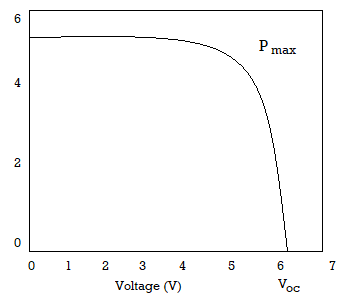
Figure 23: I-V characteristics of a solar panel
When a PV array is connected to a load directly the system’s operating point will be at the intersection of I-V curve of PV array and load. Under most conditions, this operating point may not be at the PV array’s MPP (represented as point A), which is clearly shown in figure.
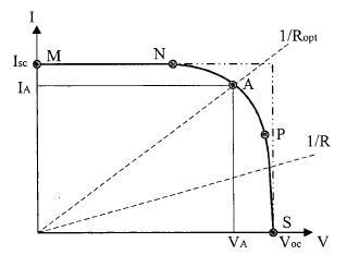
Fig 24. IV curve of a PV cell under standard conditions
Fundamental Parameters of Photovoltaic Cell are
ISC (Short Circuit Current): It is the PV output current under Short-Circuit condition.
Voc (Open Circuit Voltage): It is the voltage value of PV cell when its output current is zero.
MPP (Maximum Power Point): It represents the maximum power level of a PV’s output under specific condition. The point A in Figure 4 shows this point.
The output characteristics of photovoltaic cells are non-linear, and the value for optimum operating point varies constantly with changes in the environmental conditions of solar irradiation and cell temperature. The relations between power and voltage (P-V curve) are shown in Figure
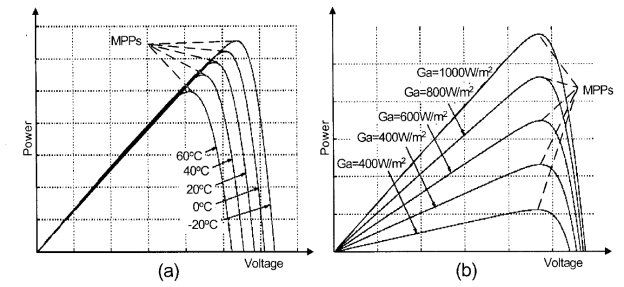
Fig 25(a) PV characteristics of a photovoltaic array for various values of temperature at constant irradiation. (b) PV characteristics of a photovoltaic array for various values of insolation at constant temperature.
One significant problem with photovoltaic power system is the probable mismatch between the operating system characteristics of the load and the PV array. Maximum Power point Tracking is specifically designed to remove the mismatch.
As shown below the standard I-V curve for a PV panel, with X-axis representing voltage and Y axis representing current. When a PV array is connected to a load directly, the system’s operating point will be at the intersection of IV curves of PV array and load. Under most conditions, this operating point may not be at the PV array’s maximum power point. Furthermore, the operating point varies constantly with changes in the environmental conditions of solar irradiations and cell temperature.
Figure (a) shows the MPP shifts with cell temperature change, and fig (b) represents that it moves with insolaion changes. In reality the change of array temperature moves the MPP in a large range along X axis and changing irradiation varies array power output dramatically with little maximum opearting voltage (VMPOP) shift.
It is impossible to consider solar isolation and photovoltaic array temperature separately as they are highly coupled under ordinary opearting conditions. This statement implies that an increase in the insolation on PV module will be accompanied by an increase in the module teperature as well. Therefore, it seems the tracking control of maximum power point is even complicated. To overcome this problem, a power interface (such as DC/DC converter or DC/AC inverter) controlled by maximum power point tracking (MPPT) controller can be used to maintain the PV array’s operating point at the maximum power operating point (MPOP).
References:
- Power Electronics by M.D Singh Second Edition
- Fundamentals of Power Electronics by S.K Bhattacharya.