UNIT 1
Semiconductor Devices and Applications
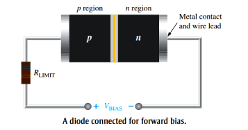
V Barrier
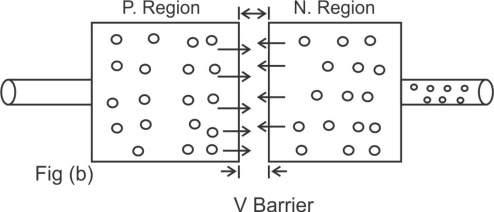
The effect of forward bias on the depletion region:-
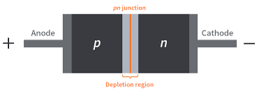

Depletion Region
The Effect of the Barrier Potential during forward bias:-
REVERSE BIAS:-
Reverse bias is the condition the essentially prevents current through the diode.
 P-region N- region

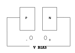
A Diode connected for Reverse Biased-

- As more of the N & P regions become depleted of majority carriers, the electric field between the positive and -ve ions increase in strength the depletion region equals the bios vtg .this point the transition current essentially ceases except for a small reverse current that can usually be neglected.
Reverse Current
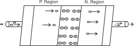
The Extremely small reverse current in a reverse biased diode is due to the minority carriers from thermally generated
e=hole pairs
The Diode - Before doping the p-type & N-type consisting silicon material atom acting as a neutral.
IF a piece of intrinsic silicon is doped so that part is n-type and the other part is p-type, a junction forms at the bounded between the two regions and a diode is created.
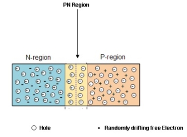
Formation of the Depletion Region

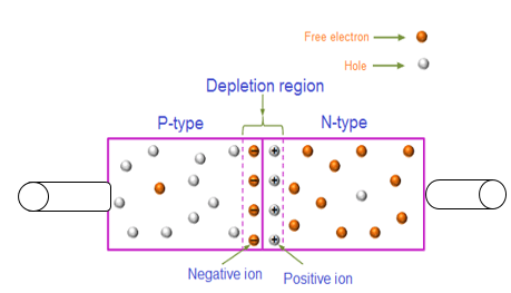
At the instant of junction formation , free electrons in the N-region near the p-n junction being to diffuse across the junction and fall into holes near the junction in the P-region.
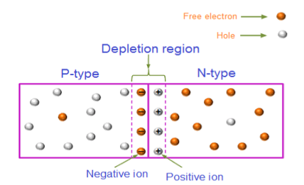
For every electron that defuse across the junction and combines with a hole , a positive charge is left in the region and a ve charge is created in the p-region firming a barriers potential. This action continues until the vtg of the barrier ripples further diffusion.
The Depletion region acts as a barriers to the farther movement of electrons across the junction
As positive ion & -ve ion across the junction produces a electric field across the junction -according to coulombs law.
The potential difference of the electric field across the depletion region is the amount of vtg required to move electronics through the electric field, this potential difference is called the barrier potential & is expressed in volt
The typical barrier potential is approximately 0.7 v for silicon & 0.3 v for germanium at 25c.
Half Wave rectifier
1) Due to the unidirectional current flow through the transformer there is a possibility of core saturation to avoid this transformer size must be increased.
2) Ripple factor is high.
3) Low rectification effecting.
4) Law TUF.
5) Law D.C O/P VTG & current.
6) Large filter component are required.
ADVANTAGES:-
1) Simple Construction.
2) Component required less.
3) Small size.
APPLICATION:-
Walkman, law cost power supply.
TRANSFORMER UTILISATION FACTOR (TUF):-It indicates how well the ilp transformer is being utilized
TUF= DC O/P Power / AC power rating of the transformer

Full Wave Rectifier
1) A centre tapped rectifier is a type of full wave rectifier that uses two diode connected to the secondary of a centre tapped transformer.
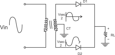
Center tapped full wave rectifier operation:-
I) During positive half cycle of i/p ac supply.
Diagram

D1.Is in forward biased & D2 is in reverse biased.
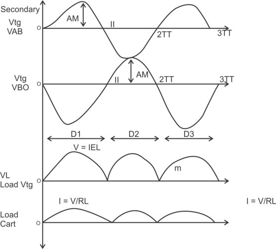
II)During -ve half cycle.

D1 Reverse biased
D2 Forward biased
ADVANTAGES
1) law ripple factor as Compared to HKR.
2)Better rectification efficiency.
3) Better TUF.
4)Higher value of average load vtg & avg load crt.
5)No possibility of transformer core saturation.
DISADVANTAGES
PIV of diode is 2vm , more size costly.
APPLICATION
I) Battery charges.
2)power supply at laboratory, high current, electronic ckt.
Being that capacitors have offer very high resistance to low frequency signals and low resistance to high frequency signals, it acts as a high pass filter, which is a filter which passes high frequency signals and blocks low frequency signals.
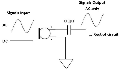
Many times in a circuit, both DC and AC signals need to be both be used in a circuit, at least at a certain stage of the circuit. However, at another stage, in the circuit, we may only want AC signals and the DC taken out. An example of such a circuit is a microphone circuit. We need DC as input to the microphone for it to be able to be powered on and we need AC as input, which represents the voice signal or music, etc. which we want the microphone to record.
We use a capacitor to filter out the DC signal.
We do this by placing the capacitor in series. In this configuration, which is the circuit you see below, this is a capacitive high-pass filter. Low frequency, or DC, signals will be blocked.
Usually, a 0.1µF ceramic capacitor, or value around that range, is placed after the signal that contains both DC and AC signals. And this capacitor filters out the DC component so that only AC goes through.
PRINCIPLE OF OPERATION: - A zener diode can be forward biased or reverses biased. its operation in the forward biased mode is same as that of a p-n junction diode but its operation in the reverse biased mode is sustainably deferent.

1.5 Zener diode as voltage regulator
Zener Diodes can be used to produce a stabilized voltage output with low ripple under varying load current conditions. By passing a small current through the diode from a voltage source, via a suitable current limiting resistor (RS), the zener diode will conduct sufficient current to maintain a voltage drop of Vout.
Resistor, RS is connected in series with the zener diode to limit the current flow through the diode with the voltage source, VS being connected across the combination. The stabilized output voltage Vout is taken from across the zener diode.
The zener diode is connected with its cathode terminal connected to the positive rail of the DC supply so it is reverse biased and will be operating in its breakdown condition. Resistor RS is selected so to limit the maximum current flowing in the circuit.
With no load connected to the circuit, the load current will be zero, ( IL = 0 ), and all the circuit current passes through the zener diode which in turn dissipates its maximum power. Also a small value of the series resistor RS will result in a greater diode current when the load resistance RL is connected and large as this will increase the power dissipation requirement of the diode so care must be taken when selecting the appropriate value of series resistance so that the zener’s maximum power rating is not exceeded under this no-load or high-impedance condition.
The load is connected in parallel with the zener diode, so the voltage across RL is always the same as the zener voltage, ( VR = VZ ). There is a minimum zener current for which the stabilization of the voltage is effective and the zener current must stay above this value operating under load within its breakdown region at all times. The upper limit of current is of course dependent upon the power rating of the device. The supply voltage VS must be greater than VZ.
Numerical:
A 5.0V stabilized power supply is required to be produced from a 12V DC power supply input source. The maximum power rating PZ of the zener diode is 2W. Using the zener regulator circuit above calculate:
a). The maximum current flowing through the zener diode.
Maximum current = Watts/ Voltage =2W/5V =400mA
b). The minimum value of the series resistor, RS
 = 17.5 Ω
c). The load current IL if a load resistor of 1kΩ is connected across the zener diode.

d). The zener current IZ at full load.
Iz =Is -Il =440mA – 5mA = 395mA
There are two types of voltage regulators −
Fixed voltage regulator
A fixed voltage regulator produces a fixed DC output voltage, which is either positive or negative. In other words, some fixed voltage regulators produce positive fixed DC voltage values, while others produce negative fixed DC voltage values.
78xx voltage regulator ICs produce positive fixed DC voltage values, whereas, 79xx voltage regulator ICs produce negative fixed DC voltage values.
The following points are to be noted while working with 78xx and 79xx voltage regulator ICs −
- The first and second pins of 78xx voltage regulator ICs are used for connecting the input and ground respectively.
- The first and second pins of 79xx voltage regulator ICs are used for connecting the ground and input respectively.
Adjustable voltage regulator
An adjustable voltage regulator produces a DC output voltage, which can be adjusted to any other value of certain voltage range. Hence, adjustable voltage regulator is also called as a variable voltage regulator.
The DC output voltage value of an adjustable voltage regulator can be either positive or negative.
*BJT:- The BJT is constructed with the three draped semiconductors region’s separate by two Pn junctions as shown below
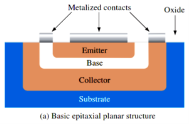
-Basic epitaxial planner structures.
-Three terminal with region’s are called emitter, base and collector.
-The physical representation of the two types of BJT’s,
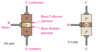
One type consists between two regions separated by a P region (npn) and other type consists of two p regions separated by an n region (pnp).
-The Pn junction joining the base region and the emitter region is called the base emitter junction.
-The Pn junction joining the base region and the collector region is called the base collector junction.
-The base region is lightly doped and very thin compared to the heavily doped emitter and the moderately doped collector regions.
*Base Transistor Operation:-
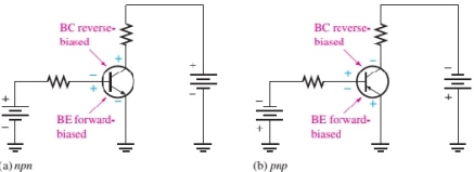
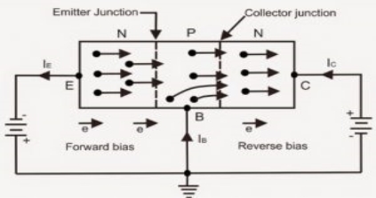
In order for the transistor to operate properly as an amplifier the two pn junction must be correctly biased with the external D.C vtg.
-The next figure shows the proper bias arrangement for both the npn and pnp transistors for active operation as an amplifier.
-In both the cases the base emitter
(BE) junction is forward biased & the base collector junction (BC) junction is reverse biased
Transistor Current:-
Transistor’s Characteristic’s and parameters:-
-The transistors is connected to d.c bias vtg for both the npn&pnp types VBB forward biases the base emitter junction &Vcc reverse biases the base collector junction.
*Biasing conditions for different regions of operation:-
Sr. no | Region of operation | BE junction | CB junction | work |
1 | Cutoff region | R.B | R.B | S/w |
2 | Active region | F.B | R.B | Ampr |
3 | Saturation region | F.B | F.B |
|
Transistor’s Configuration:-
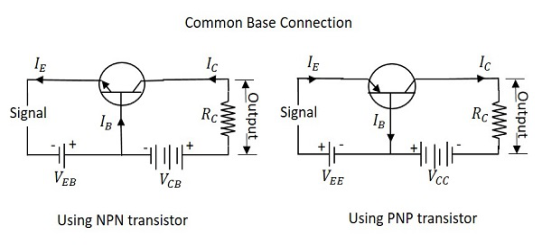
1) Common Base configuration(C.B)
2) Common emitter Configuration(C.E)
3) Common Collector Configuration(C.C)
Common Base configuration(C.B):-

-The I/p is applied between the emitter and the base. The base acts as a common terminal between the I/p and o/p.
-The input vtg is therefore VEB and the input current is IE.
-The output is taken between the collector and the base therefore the output vtg is VCB and the output current is IC.
* Current relation’s in CB configuration:-
-The collector current is IC of the common base configuration is given by
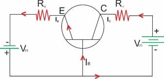
Ic=Ic(INI)+ICBO
-Where the Ic(INI) called the injected collectors current and it is due to the number of electrons crossing the collectors base junction.
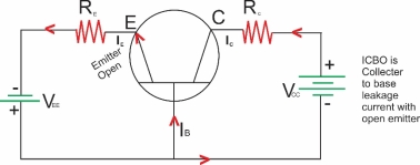
-ICBO :- This is the reverse saturation current flowing due to the minority carrier’s between the collector and base when the emitter is open
-ICBO flow’s due to the reverse biased collector’s base junction. As ICBO negligible as compared to Ic(INI) we can neglect it in practice.
.’. Ic=Ic(INI)………………………practically
Ic=ICBO………………with emitter open
-Since the ICBO flow’s due to terminally generated minority carrier’s it increases with increase the temperature.
-It doubles it’s value for every 100c rise in temperature.
-Current amplification factor or current gain (ddc):-
Current amplification factor or current gain is the ratio of collector current due to the injection to the total emitter current
αd.c = Ic(INI)
-The value of the ddc for CB configuration will always be less than 1.This is because
Ic(INI)<IE.
-Typically the value of d.d.c ranges between 0.95 to 0.995 depending upon the thickness of the base region
-Larger the thickness of the base region smaller the value of the d.d.c
Ic(INI)=d.d.c.IE
Hence the expression for IC is given by
IC=αd.c IE + ICBo--------------------I
But the ICBo is negligibly small
IC d.d.c IE
* Expression for IB:-
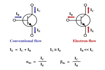
IE=IB+IC
IE=αd.cIE+ICBo+IB…………………from I
IB=(1-αd.c)IE-ICB
Neglecting ICBo
IB=(1-αd.c)IE
1. Input Characteristic:-
A. Input Characteristic: is always a graph of input current verses input vtg. For common base (CB) configuration input current is the emitter current (IE) & I/p vtg. is the emitter to the base vtg (VEB)
The I/p Characteristic is plotted at a constant O/p vtg. VCB

B. Output Characteristic:
Output Characteristic is always a graph of O/p current versus O/p Vtg.
For the CB configuration the O/p current is collector current (IC) of the output voltage is collector to base vtg. (VCB)
Output Characteristic is plotted for a constant value of I/p current (IE)
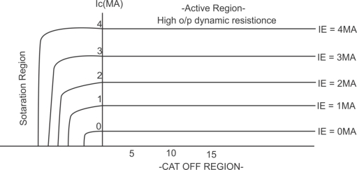
O/p Characteristic of a n-p-n transistor in CB Configuration
Dynamic O/p resistance (ro)
ro =  / I
/ I  constant
in the active region Ic does not depend on VCB. It depends only on the I/p current IE. That is why the transistor is called as a current controlled or current operated device.
Feature of CB configuration :

Common Emitter (CE) configuration
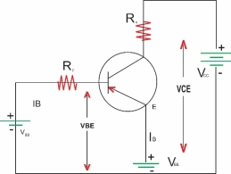
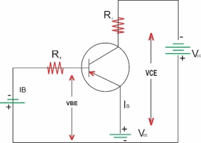
The important points about the CE
Configurations are as follows: the emitter acts as a common terminal between I/p and output. The /p Vtg. Is called between base and emitter
Hence VBE is the I/p Vtg. And IB is the input current.
The O/p is taken between the collector and emitter. There for VCE is the O/p Vtg. And IC is the O/p current.
In order to operate the transistor in its active region the base emitter (BE) junction is forward biased and collector base junction is reverse biased.
IE = IC + IB
Where IC =  d.c.IE + ICBO
Rearrange this eqn to get
IC – ICBO =  d.c.IE
 -
-  = IE = IC + IB
 ] = IB -
IC  ] = IB +
 ] +
] + 


The value of  is match higher than
 =
= 
 =
=  =
=  =
= 
IC =  IB +
IB +  …….. I
But  =
= 
 1 +
1 +  =
=  + 1
+ 1
1 +  =
= 
 1 +
1 +  =
= 
Put in eqn I
IC =  IB + (1+
 ICBO above eqn can be expressed as
IC =  IB + ICEO
Where ICEO is the reverse saturation current for the CE configuration which is given by
ICEO = (1+  ) ICBO
The Reverse leakage current of a transistor operating
in the LE configuration is denoted by
ICEO = (1 +  ) ICBO
As the value of 

put IB = 0
 IC = (1 +
The Reverse leakage current (ICEO)
Increases with increase in the temperature this current flows in the same direction as that of IC there for the collector current IC will increase with increase in temperature even when IB is constant
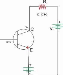
This is called as thermal instability so in CE configuration thermal stabilizing CKT must be included.

We know that
IC 
Though ICEO is large it is much smaller as compared to . Therefor the eqn for IC gets modified as
 C =
C = 


We know that
 but
but
 =
=  =
= 
 =
= 
Similarly we can obtain the expression for  d.c in terms of
  as follows
 d.c =
d.c =  but
but 
=
Multiply & divide numerator & denominator for by IE
 d.c =
d.c = 
 d.c =
d.c = 
 =
= 
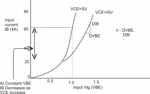
The value of dynamic input resistance ri is low for the CE configuration but it is not as low as that of CE configuration
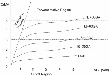
IB = 0 is cutoff region.
The collector current IC increases slightly with increase in the vtg.VCE. However the collector current is largely dependent on the base current IB
At fixed value of VCE if IB is increased then it will cause IC to increase substantially.
This is because IC = BIB this relation is true only for the active region of operation.

