UNIT-2
PN JUNCTION DIODE
P-N JUNCTION DIODE
A P-N Junction Diode is formed by doping one side of a piece of silicon with a P-type dopant (Boron) and the other side with a N-type dopant (phosphorus). Ge can be used instead of Silicon. The P-N junction diode is a two-terminal device. This is the basic construction of the P-N junction diode. It is one of the simplest semiconductor devices as it allows current to flow in only one direction.
ZERO BIASED CONDITION
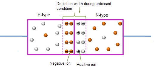
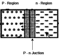
In this case, no external voltage is applied to the P-N junction diode; and therefore, the electrons diffuse to the P-side and simultaneously holes diffuse towards the N-side through the junction, and then combine with each other. Due to this an electric field is generated by these charge carriers. The electric field opposes further diffusion of charged carriers so that there is no movement in the middle region. This region is known as depletion width or space charge.
|
Figure 1: Unbiased or zero biased PN Junction Diode
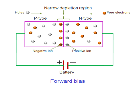
In the forward bias condition, the positive terminal of the battery is connected to the P-Type material and the negative terminal of the battery is connected to the N-type material. This connection is also called as giving positive voltage.
|
Figure 2: Forward bias
Electrons from the N-region cross the junction and enters the P-region. Due to the attractive force that is generated in the P-region the electrons are attracted and move towards the positive terminal. Simultaneously the holes are attracted to the negative terminal of the battery. By the movement of electrons and holes current flows. In this condition, the width of the depletion region decreases due to the reduction in the number of positive and negative ions.
If this external voltage Vf becomes greater than the value of the potential barrier, approx. 0.7 volts for silicon and 0.3 volts for germanium, the potential barriers opposition will be overcome and current will start to flow.
This is because the negative voltage pushes or repels electrons towards the junction giving them the energy to cross over and combine with the holes being pushed in the opposite direction towards the junction by the positive voltage. This results in a characteristics curve of zero current flowing up to this voltage point, called the “knee” on the static curves and then a high current flow through the diode with little increase in the external voltage as shown in I-V characteristics.
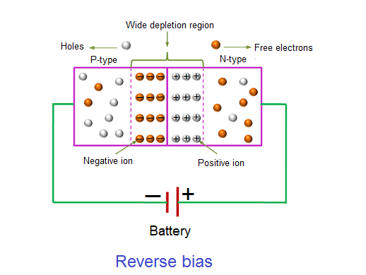
In the reverse bias condition, the negative terminal of the battery is connected to the P-type material and the positive terminal of the battery is connected to the N-type material. This connection is also known as giving negative voltage.
|
Figure 3: Reverse bias
The positive voltage applied to the N-type material attracts electrons towards the positive electrode and away from the junction, while the holes in the P-type end are also attracted away from the junction towards the negative electrode.
The net result is that the depletion layer grows wider due to a lack of electrons and holes and presents a high impedance path, almost an insulator. The result is that a high potential barrier is created thus preventing current from flowing through the semiconductor material.
This condition represents a high resistance value to the PN junction and practically zero current flows through the junction diode with an increase in bias voltage. However, a very small leakage current does flow through the junction which can be measured in micro-amperes, ( μA ).
If the reverse bias voltage Vr applied to the diode is increased to a sufficiently high enough value, it will cause the diode’s PN junction to overheat and fail due to the avalanche effect around the junction. This may cause the diode to become shorted and will result in the flow of maximum circuit current, and this shown as a step downward slope in the reverse static characteristics curve in I-V characteristics.
I-V CHARACTERISTICS OF PN JUNCTION DIODE
The I-V Characteristic Curves, which is short for Current-Voltage Characteristic Curves or simply I-V curves of an electrical device
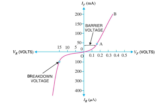
The application of a forward biasing voltage on the junction diode results in the depletion layer becoming very thin and narrow which represents a low impedance path through the junction thereby allowing high currents to flow. The point at which this sudden increase in current takes place is represented on the static I-V characteristics curve above as the “knee” point. The current starts increasing with increase in voltage. At knee voltage current shows a sharp increment in its magnitude. This behaviour is mentioned above. As large current flow in forward biasing so we measure this current in mA.
When a junction diode is Reverse Biased, the thickness of the depletion region increases and the diode acts like an open circuit blocking current flow. So only a very small leakage current will flow.
|
Figure 4: I-V characteristics
STEP JUNCTION
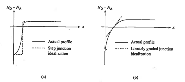
Fortunately, only the doping variation in the immediate vicinity of the metallurgical junction is of prime importance. Surprisingly accurate results can be obtained using rather idealized doping profiles.
|
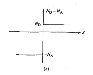
Figure 5: Idealized doping profiles (a) Step junction (b) linearly graded junction.
The two most common idealizations are Step junction and linearly graded junction. The more appropriate of the two idealizations depends on the slope of the actual doping profile at the metallurgical junction and the background doping of the starting wafer.
The step junction is an acceptable approximation to an ion-implantation or shallow diffusion into starting wafer, whereas the linearly graded profile would be more appropriate for deep diffusions into a moderate to heavily doped starting wafer. In most pn junction analyses we are dealing with; we arbitrarily invoke the step junction idealization to minimize the mathematical complexity of the analysis.
Key Takeaways
- A P-N Junction Diode is formed by doping one side of a piece of silicon with a P-type dopant (Boron) and the other side with a N-type dopant (phosphorus). Ge can be used instead of Silicon.
- Zero biased condition is the case when no external voltage is applied to the P-N junction diode.
- In the forward bias condition, the positive terminal of the battery is connected to the P-Type material and the negative terminal of the battery is connected to the N-type material. This connection is also called as giving positive voltage.
- In the reverse bias condition, the negative terminal of the battery is connected to the P-type material and the positive terminal of the battery is connected to the N-type material. This connection is also known as giving negative voltage.
- The two most common idealizations are Step junction and linearly graded junction.
The Voltage drop across the depletion region under equilibrium conditions, known as the built-in potential (Vbi), is a junction’s parameter of sufficient importance to merit further consideration.
We will now find a relationship for Vbi. Consider a non-degenerately doped pn junction maintained under equilibrium conditions with x = 0 positioned at the metallurgical boundary. The ends of the equilibrium depletion region are taken to occur at — xp and xp on the p- and n-sides of the junction respectively
We know
Integrating across the depletion region gives
……………(2) Under equilibrium conditions.
Solving for ξ in equation (3) and making use of the Einstein relationship. We obtain Substituting Equation (4) into Equation (2), and completing the integration then yields ……………(5) For the specific case of a non-degenerately doped step junction where ND and NA are the n- and p-side doping concentrations, one identies. and therefore
It is useful to perform a sample computation to gauge the relative magnitude of the built in voltage. Choosing ND= NA = 1015/ cm3 and a Si diode maintained at 300 K, One computes Vbi= (0.0259) ln(1030/1020) From the energy band diagram, we observed
Clearly, For a Non-degenerately doped diode bosh (Ei — EF)p-side, and (EF — Ei)n-side are less than EG/2, making Vbi < EG/q Moreover, in a Non-degenerately doped step junction under equilibrium conditions,
Equations (12 and13) and Equation (9) are valid only for Non-degenerately dopings, there are no doping-related restrictions on the validity of Equation (11).
|
Key Takeaways
- The Voltage drop across the depletion region under equilibrium conditions, known as the built-in potential (Vbi), is a junctions parameter of sufficient importance to merit further consideration.
- It is given by
|
DEPLETION WIDTH
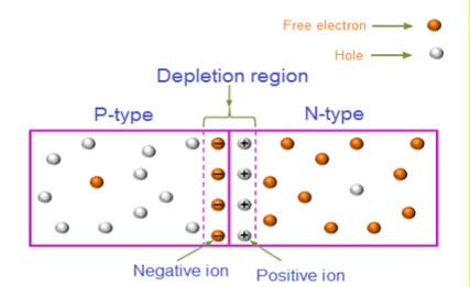
Depletion region or depletion layer is a region in a P-N junction diode where no mobile charge carriers are present. Depletion layer acts like a barrier that opposes the flow of electrons from n-side and holes from p-side.
|
Figure 6: Depletion region
At the instant of junction formation , free electrons in the N-region near the p-n junction being to diffuse across the junction and fall into holes near the junction in the P-region. The width of depletion region is depends on the amount of impurities added to the semiconductor.
|
Figure 7: Depletion region
The Depletion region acts as a barriers to the farther movement of electrons across the junction
As positive ion & -ve ion across the junction produces a electric field across the junction -according to coulombs law.
The potential difference of the electric field across the depletion region is the amount of voltage required to move electronics through the electric field, this potential difference is called the barrier potential & is expressed in volt
The typical barrier potential is approximately 0.7 v for silicon & 0.3 v for germanium at 25c.
Depletion width of two sided abrupt junction can be calculated by the following formula

For one sided abrupt junction it is given by the following formula

DEPLETION APPROXIMATION
The depletion approximation simplifies obtaining closed-form solutions to the Poisson's equation.
The depletion approximation one of the important and widely used simplifying approximations in the modeling of devices.
Let start with solving the question what is the need to understand the depletion approximation. Let us take a look at the one-dimensional Poisson equation given as
 …………(1)
The doping profile, ND - NA, appearing in the equation is assumed to be known. However, to write down ρ as a function of x, we need to solve the differential equation for ξ versus x, and eventually obtain V versus x. We must have known the explicit expressions for the carrier concentrations as a function of x. Unfortunately, the carrier concentrations in ξ  0 regions, like the pn junction depletion region, are not specified prior to solving Poisson's equation.
The depletion approximation provides a simple, nearly universal way of obtaining approximate solutions without prior knowledge of the carrier concentrations.
We have already established the basis for the depletion approximation. A prominent feature of the qualitative solution was the appearance of a nonzero charge density straddling the metallurgical junction. This charge arises because the carrier numbers are reduced by diffusion across the junction. The carrier "depletion" tends to be greatest in the immediate vicinity of the metallurgical boundary and then tails off as one proceeds away from the junction.
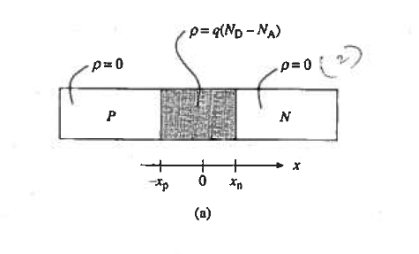
The depletion approximation introduces an idealization of the actual charge distribution. The approximation has two components that can be stated as follows:
- carrier concentrations are assumed to be negligible compared to the net doping concentration in a region — xp
 x
x  xn, straddling the metallurgical junction.
 - The charge density outside the depletion region is taken to be identically zero.
|
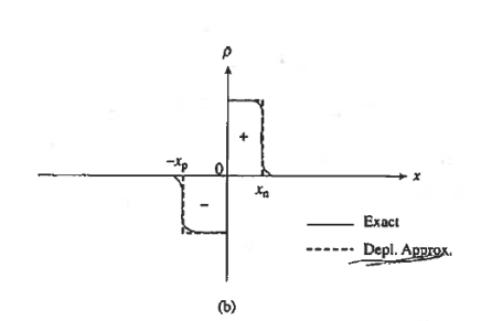
Figure 8: (a) Depletion approximation (b) Depletion approximation applied to step junction
The Depletion approximation is summarized pictorially in figure 8(a) and is illustrated assuming a step junction in figure 8(b). When Depletion approximation is applied the one dimensional poisson’s equation simplifies to
|
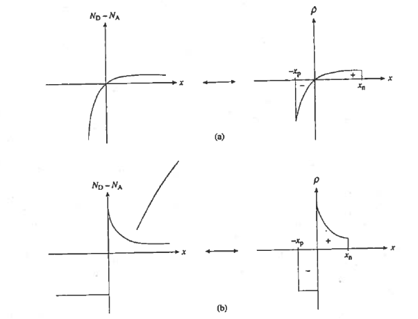
Note that, except for the values of — xp and xn, the charge density is specified by applying the depletion approximation. Moreover, the charge density will have precisely the same functional form as ND - NA within the depletion region.
|
Figure 9: versus x plots
Figure is represented to emphasize this last point by showing the  versus x plots associated with sample doping profile of a moderately complex nature.
Key Takeaways
The depletion approximation simplifies obtaining closed-form solutions to the Poisson's equation.
The depletion approximation one of the important and widely used simplifying approximations in the modeling of devices.
one-dimensional Poisson equation given as

The approximation has two components that can be stated as follows: 1. carrier concentrations are assumed to be negligible compared to the net doping concentration in a region — xp  x
x  xn, straddling the metallurgical junction. 2. The charge density outside the depletion region is taken to be identically zero.
ELECTROSTATIC RELATIONSHIPS
The development of quantitative relationships for the electrostatic variables deals with the step junction and is presented in detail not only to obtain the desired relationships but also to establish the derivational procedures that can be applied to other doping profiles.
|
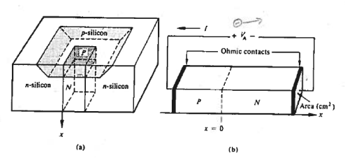
Figure 10: (a) Sketch of o physical diode. (b) One-dimensional diode subjected to the applied voltage, coordinates, and contact specifications.
Assumptions
Major features of the pn junction diode subject to analysis are identified in Figure 10.
- All variables are taken to be functions only of x, the coordinate normal to the semiconductor surface.
- The device is thus said to be "one-dimensional"; obvious two-dimensional effects associated with the lateral ends of a real device are assumed to be negligible.
- For the electrostatic analysis, x = 0 is positioned at the metallurgical boundary.
- External contacts to the ends of the diode are specified to be "ohmic" in nature.
- By definition, a negligible portion of an externally applied voltage appears across an ohmic contact.
- Symbol VA is used for the applied voltage. The subscript A distinguishes the applied voltage from the internal junction voltage.
- In the initial development VA is set equal to zero, or equivalently, the device is assumed to be in equilibrium.
STEP JUNCTION WITH VA = 0
Solution for ρ
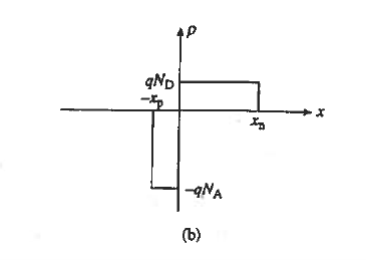
We consider a step junction under equilibrium conditions. NA is drawn greater than ND in the Figure 11(a) sketch of the doping profile for the sake of illustration. As summarized in Figure 11(b), invoking the depletion approximation yields the charge density solution
|
The values of xn and xp are not known at this point but will be determined later in the analysis.
Solution for ξ
Substituting the charge density solution into Poisson's equation gives the equations to be solved for the electric field.
ξ = 0 far from the metallurgical boundary and therefore ξ = 0 everywhere outside of the depletion region. Since must also vanish right at the edges of the depletion region, ξ = 0 at x = — xp and ξ = 0 at x = xn respectively become the boundary conditions for the differential equations (1). Separating variables and integrating from the depletion region edge to an arbitrary point x, one obtains for the p-side of the depletion region
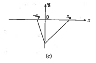
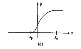
Figure 11: Step Junction solution. Depletion approximation based quantitative solution for the electrostatic variables in pn step junction at equilibrium condition (VA= 0) (a) Step junctions profile. (b) Charge density, (c) electric field, and (d) electric potential as a function of position x.
Similarly for the n-side
|
The electric field solution is plotted in Figure 11(c). it is clear that
- Within the depletion region the field is always negative and exhibits a linear variation with position.
- The electric field was taken to be continuous at x = 0; the p- and n-side solutions were simply matched at the metallurgical boundary.
From Electricity and Magnetism, we know the electric field will be continuous across a boundary as long as a sheet of charge does not lie along the interface between the two regions. If the equations (4) and (6) expressions for the electric field are evaluated at x = 0 and equated, the continuity of the electric field is found to require
NAXp = NDXn ……….(7)
For those familiar with Gauss' law, the fact that ξ = 0 outside the depletion region means the total charge within the depletion region must sum to zero, or the minus charge on the p-side of the junction must balance the plus charge on the n-side of the junction.
Applied to the step junction ρ versus x plot in Figure 11(b), the balance of charge requires the rectangular areas on the p- and n-sides of the junction to be equal, or (qNAXp = qNDXn)
Thus Equation (7) gives the fact that the total charge within the depletion region must sum to zero.
Solution for V
Since ξ = — dV/dx, the electrostatic potential is obtained by solving
|
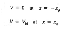
With the arbitrary reference potential set equal to zero at x = —xp, and remembering the voltage drop is Vbi across the depletion region under equilibrium conditions, Equation (8) are respectively subject to the boundary conditions given as
Separating variables and integrating from the depletion region edge to an arbitrary point x, one obtains for the p-side of the depletion region
For n side
|
The electrostatic potential solution given by Equations (11) and (13) is plotted in Figure 11(d). The V versus x dependence is quadratic in nature, with a concave curvature on the p-side of the junction and a convex curvature on the n-side of the junction.
Paralleling the ξ -field procedure, Fig. 5.9(d) was constructed simply by matching the p- and n-side solutions at x = 0. The assumed continuity of the electrostatic potential at x = 0 is justified because there is no dipole layer (closely spaced sheets of plus and minus charge) along the metallurgical boundary.
The Equations (11) and (13) expressions for the potential are evaluated at x =0 and equated, one obtains
Solution for xp and xn The electrostatic solution is not complete until the values of xp and xn are determined. Specifically, xp and xn are the only unknowns in Equations (7) and (14). Using (7) in (14) we can found xn.
And after solving further the value of xp comes to be Thus we get
|
W is the total width of the depletion region, better known simply as the depletion width.
ELECTROSTATIC RELATIONSHIP (CHARGE DENSITY, DEPLETION WIDTH, POTENTIAL, ELECTRIC FIELD) FOR VA  , VA
, VA  0 AND VA
  0,
0,
Step Junction with VA 
For the practical purpose the solution for the electrostatic variables must be extended to VA  .
.
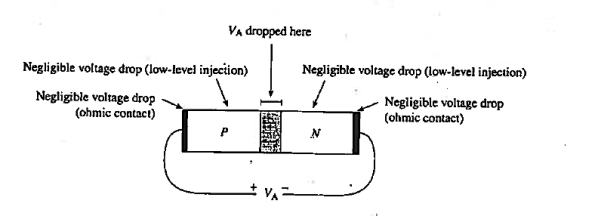
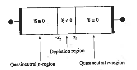
Consider the diode in Figure 12 with a voltage VA  applied to the diode terminals. This voltage must be dropped somewhere inside the diode. However, in a well-made device a negligible portion of the applied voltage appears across the contacts to the device.
More-over, under low-level injection conditions (reasonable current levels) the resistive voltage drop across the quasineutral p- and n-regions extending from the contacts to the edges of the depletion region will also be negligible.
The applied voltage must therefore be dropped across the depletion region. When VA> 0. this externally imposed voltage drop lowers the potential on the n-side of the junction relative to the p-side of die junction. Conversely, when VA < 0, the potential on the n-side increases relative to the p-side.
|
Figure 12: Voltage drops internal to a diode resulting from external applied voltage.
In other words, the voltage drop across the depletion region, and hence the boundary condition at x = xn, becomes Vbi - VA.
Since the only modification to the formation of the problem is a change in one boundary condition, the VA  electrostatic relationships can be extrapolated from the VA = 0 relationships by simply replacing all explicit appearances of Vbi by Vbi - VA.
Making the indicated substitution yields the VA  solution for the electrostatic variables given in Equations.
For -xp
For
Thus depletion width become
|
To prevent so imaginary result, VA is obviously restricted to VA  Vbi in Equations (20), (23) and (24). The formulation fails because a large current begins to flow, and quasineutral region voltage drops cannot he neglected, when VA approaches Vbi.
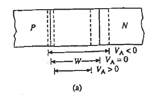
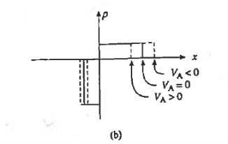
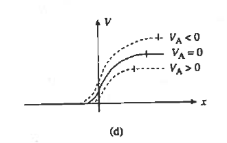
Let us see how the electrostatic variables change as a function of the applied bias. Examining the (20) and (23) relationships for xp and xn, we conclude these widths decrease under forward biasing (VA > 0) and increase under reverse biasing ( VA < 0).
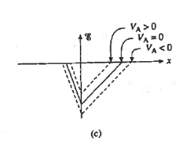
The changes in xp and xn likewise translate into changes in the electric field. As deduced from Equations (18) and (21), a smaller xp and xn under forward biases cause the ξ -field to decrease everywhere inside the depletion region while-the larger xp and xn associated with reverse biases give rise to a larger ξ -field.
This conclusion is also reasonable from a physical standpoint. A decreased depletion width when VA > 0 means less charge around the junction and a correspondingly smaller ξ-field. On the other hand VA<0, creates a larger space charge region and a bigger electric field,
The potential given by Equations (19) and (22) decreases at all points when VA > 0 and increases at all points when VA < 0. The potential hill shrinks in both size and x-extent under forward biasing, whereas reverse biasing gives rise to a wider and higher potential hill.
This is summarized graphically in figure 13.
|
|
|
|
Figure 13 : Effect of forward and reverse biasing on the (a) deptetion width, (b) charge density (c) electric field and (d) electric potential inside a pn junction diode.
|
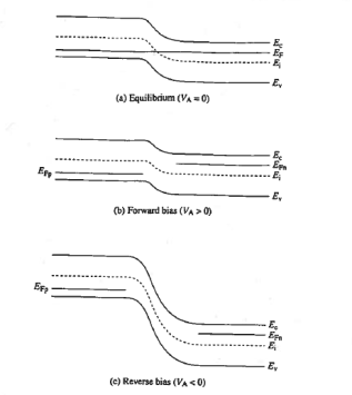
Figure 14: pn junction energy band diagrams. (a) Equilibrium (VA = 0), (b) forward bias (VA>0), and (c) reverse bias (VA< 0).
We come across that the energy band diagram under equilibrium condition. Conceptually taking the upside-down of the potential plots and appropriately modifying the equilibrium energy band diagram—smaller depletion width and smaller hill for forward bias, larger depletion width and larger hill for reverse bias—yields the diagrams for forward and reverse bias respectively pictured in Figure 14(b) and (c).
From figure it is clear the Fermi level is omitted from the depletion region because the device is no longer in equilibrium and a single level cannot be used to describe the carrier concentrations in this region. In fact, the levels labelled EFn and EFp occupying the former position of the Fermi level in the quasineutral regions, are actually majority-carrier quasi-Fermi levels.
However, the deviation from equilibrium in the non-depleted portions of the diode is normally small, especially far from the junction, and it is therefore acceptable to continue using the EF designation.
EFp - EFn = qVA
Key Takeaways
- The development of quantitative relationships for the electrostatic variables deals with the step junction
- In the initial development VA is set equal to zero, or equivalently, the device is assumed to be in equilibrium.
- Depletion width For VA =0 is given by
|
- With a voltage VA
 applied to the diode terminals. This voltage must be dropped somewhere inside the diode.
 - Thus depletion width become With a voltage VA

|
- A smaller xp and xn under forward biases cause the ξ -field to decrease everywhere inside the depletion region while-the larger xp and xn associated with reverse biases give rise to a larger ξ -field.
- A decreased depletion width when VA > 0 means less charge around the junction and a correspondingly smaller ξ-field.
- On the other hand VA<0, creates a larger space charge region and a bigger electric field,
- The potential decreases at all points when VA > 0 and increases at all points when VA < 0.
- The Fermi level is omitted from the depletion region because the device is no longer in equilibrium and a single level cannot be used to describe the carrier concentrations in this region.
- The levels labelled EFn and EFp occupying the former position of the Fermi level in the quasineutral regions, are actually majority-carrier quasi-Fermi levels.
Qualitative Derivation
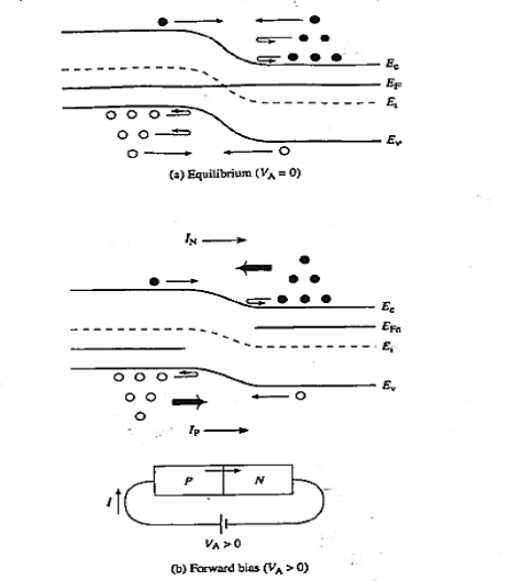
Consider the equilibrium energy band diagram for a pn junction shown in Figure. The groups of dots (•) and circles (0) added to the figure to describe the carrier distribution on the two sides of the junction.
On the quasineutral n-side of the junction there are a large number of electrons and a few holes. There is exponential decrease in the electron population as one progresses upward into the conduction band. Conversely, on the quasi neutral p-side of the junction there are a high concentration of holes and a small number of electrons. The hole population drops off in a roughly exponential fashion as one moves downward into the valence band.
The envisioned electrons and holes have thermal energy and are of course moving around inside the semiconductor. Concentrating first on the n-side electrons, we see that most of these carriers have insufficient energy to "climb" the potential hill. Excursions into the depletion region merely result in the lower-energy carriers being reflected back toward the n-side quasineutral region. However, there will be some high-energy electrons that can surmount the hill and travel over to the p-side of the junction.
This can be seen as the diffusion of electrons from the high-electron population n. side of the junction to the low-electron population p-side of the junction.
Whereas electrons on the n-side see a potential barrier; electrons on the p-side are not restricted in any way. If a member of the small electron population on the p-side happens to wander into the depletion region, it will be rapidly swept over to the other side of the junction. Naturally-this p- to n-side drift current precisely balances the n; top-side diffusion current equilibrium conditions.
The hole situation is completely analogous. The few p-side holes that have sufficient energy to surmount the potential energy barrier and gain entry to the n-side of the junction are precisely balanced by n-side holes wandering into the depletion region and being swept over to the p side of the junction.
|
Figure 15: pn junction energy band diagram, carrier distribution, and carrier activity near the depletion region (a) equilibrium (VA = 0), (b) forward bias,
Let us now consider the forward bias situation Figure 15(b). The most significant change relative to zero bias is a lowering of the potential hill between the p and n-sides of the junction. The same number of minority carriers are still wandering into the depletion region and being swept over to the other side of the junction. However, with the potential hill decreased in size more n-side electrons and p-side holes can now surmount the hill and travel to the opposite side of the junction. This gives rise to both an electron current (IN) and a hole current (IP) directed from the p-side to the n-side of the junction.
Figure 15 (b) shows energy band diagram that the deduced current (I= IN + IP) flows in the proper direction for a forward biased diode Moreover, because the potential hill decreases linearly with the applied forward bias and concentrations vary exponentially as one progresses away from the band edges, the number of carriers that have sufficient energy to surmount the potential barrier goes up exponentially with VA.
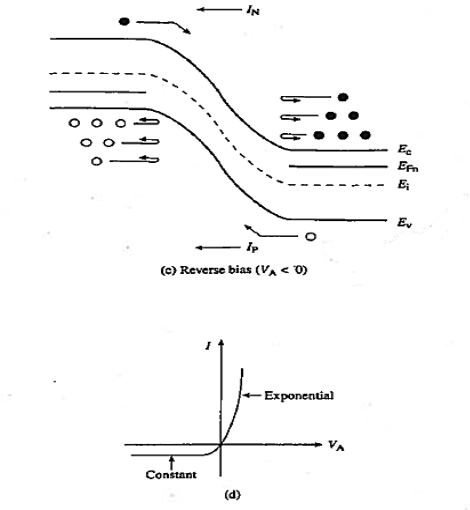
Figure 16(d) shows, the forward current is expected to be an exponentially increasing function of the applied voltage. The reverse bias situation is described by the energy band diagram in Figure 16(c). Relative to equilibrium, the major effect of the bias is to increase the potential hill between the p- and n-sides of the junction. Whereas some n-side electrons and p-side holes can surmount the hill under 'equilibrium conditions, even a very small reverse bias, anything greater than a few kT/q in magnitude, reduces the majority carrier diffusion across the junction to a negligible level. The p-side electrons and n-side holes, on the other hand, can still wander into the depletion region and be swept to the other side of the junction. Reverse biasing thus gives rise to a current flow directed from the n-side to the p-side of the junction. Being associated with minority carriers, the reverse bias current expected to be extremely small in magnitude.
|
Figure 16: pn junction energy band diagram, carrier distribution, and carrier activity near the depletion region (c) reverse biasing condition (d) Deduced form of the I—V characteristic.
Note in addition that the minority carrier drift currents are not affected by the height of the potential bill. It is the number of minority carriers wandering into the depletion region per second that determines the current flow.
The situation is similar to a waterfall. The water flowing over the falls is independent of the height of the falls. Therefore, as sketched in Fig. 6.1(d), the reverse current is expected to saturate—become bias independent—once the majority carrier diffusion currents an reduced to a negligible level of a small reverse bias. If the reverse bias saturation current is taken to be – I0, the overall 1-V dependence is concluded to be of the general form 1-V chracteristics.
 ………..(1)
Equation (1) is identical to the ideal diode equation if VA is set equal to kT/q.
In addition to essentially yielding the ideal diode equation, the foregoing analysis very nicely explains how a solid state diode manages to rectify a signal; it, how the diode passes a large current when forward biased and a very small current when reverse biased. Forward biasing reduces the potential hill between the two sides of the junction, permitting _ large numbers of majority carriers to be injected across the depletion region. Reverse biasing increases the potential hill, cutting off majority carrier injection and leaving only a residual current supplied by minority carriers.
Once, after completing the qualitative derivation and feeling rather smug about the insight provided, the author was asked. "Yes, but, doesn't the injection of majority carriers under forward bias and the extraction of minority carriers under reverse bias cause a charge build-up inside the device?" The immediate answer is that
Steady state conditions were assumed in the analysis and a charge build-up, or a change of any type, does not occur under steady state conditions.
The question, however, has deeper implications. The author concentrating solely on the carrier activity in the immediate vicinity of the depletion region, had failed to provide an overall view of carrier activity inside the device. It is the overall view that explains how injected and extracted carriers are resupplied.
QUANTITATIVE DERIVATION
Basic Assumptions
(1) The diode is being operated under steady state conditions.
(2) A non-degenerately doped step junction models the doping profile.
(3) The diode is one-dimensional.
(4) Low-level injection prevails in the quasineutral regions.
(5) There are no processes other than drift, diffusion, and thermal recombination—generation taking place inside the diode. Specifically, GL = O.
The preceding assumptions seem reasonable since they were all explicitly or implicitly invoked in establishing the pn junction electrostatics.
Let us next consider the general relationships available for computing the current. They are
|
Equation (3) gives the total current density that is constant throughout the diode but electron and hole components vary with position.
We do note that the conditions required for the one of the minority carrier diffusion equation including ξ as 0 and low-level injection, are satisfied in the quasineutral regions of the diode.
|
Figure 17: Diode electrostatics region
Quasineutral Region Considerations:
Under the assumed steady state conditions with GL = 0, the minority carrier diffusion equations appropriate for the p and n quasineutral regions are
|
Moreover since ξ = 0 and dno/dx = dpo/dx = 0, Equations (4) and (5) for the carrier current densities in the quasineutral regions simplify to
|
Unfortunately, the current density solutions so obtained are limited to non-overlapping segments of the diode. We can only determine JN(x) in the quasineutral p-region and JP(x) in the quasineutral n-region. To solve for J using Equation (3), there must be at least one point inside the diode where one knows both
The depletion region is the obvious place where JN(x) and JP(x) overlap.
Depletion Region Considerations
Continuity equation must be used in seeking solutions for the carrier currents within the ξ=0 depletion region. Under the previously specified assumptions, the continuity equations simplify to
 ………(10)
 ………(11)
Assume thermal recombination-generation is negligible throughout the depletion region so setting  |thermal R-G =0,
  |thermal R-G =0
We get dJN(x)/dx = 0 and dJP(x)/dx = 0.
JN and JP are therefore determined to be constants independent of position inside the depletion region. The constancy of the carrier currents throughout the depletion region, thus we obtain
 ……… (12)
JN(-xp) and JP(xn) can be evaluated at the edges of the depletion region. Thus we have
 ………(13)
The critical assumption that thermal recombination-generation is negligible in the depletion region can be viewed as a defining property of the ideal diode.
Boundary Conditions
The minority carrier diffusion equations require boundary conditions in order to solve. In particular, the excess minority carrier concentrations must be known at the edges of the semiconductor – at the contacts as well as the depletion region boundary.
Two boundary conditions are required
At the Ohmic Contacts:
The ideal diode is usually taken to be a "wide-base" diode. In a wide-base diode any perturbation in the carrier concentrations created at the edges of the depletion region will decay to zero before reaching the contacts. The contacts may effectively be viewed as being positioned at x = so. Thus, in the mathematical derivation
|
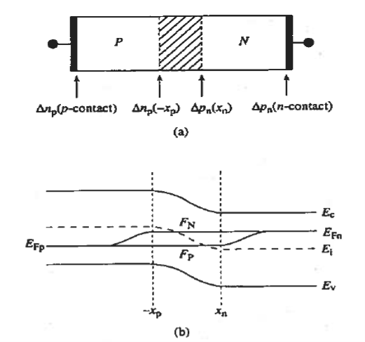
Figure 18: Boundary-condition related consideration (a) Boundary position required values. (b) Approximate variation of the quasi-Fermi levels with position inside a forward -biased diode.
The boundary conditions to be employed are
 ………(14)
At the Depletion Region Edges:
To establish the boundary conditions at the edges of the depletion region, we make use of the quasi-Fermi level formalism. We know
 ………(15)
One does not know the variation of the quasi-Fermi levels as a function of position prior to solving for the carrier concentrations inside the diode. However, as envisioned in Figure 18(b), it is reasonable to assume the FN and F, levels will vary monotonically from EFp far on the p- side of the junction to EFn far on the n-side of the junction.
Note from Figure 18(b), that the monotonic variation in the levels in turn makes
FN— FP  EFn - EFp = qVA at all points inside the diode. If the equal sign in the preceding expression for FN— FP is assumed to hold throughout the depletion region, one concludes
 ………(16)
Eq. (16) has been referred to as the "law of the junction." Evaluating Eq. (6.12) at the depletion region edges very rapidly leads to the desired boundary conditions. Specifically, evaluating Eq. (16) at the p-edge of the depletion region gives
Similarly, at n edge
|
The assumption that FN — FP = qVA throughout the depletion region, or equivalently assuming the quasi-Fermi levels are constants at FN = EFn and FP= EFP within the depletion region, is obviously central to obtaining the depletion boundary conditions and critical to the overall analysis.
Derivation
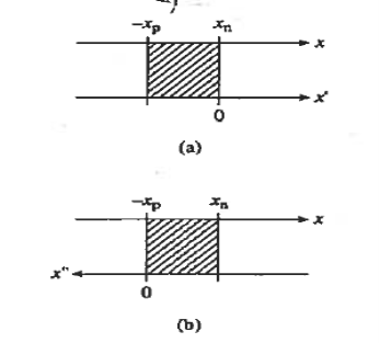
let us first work with holes on the quasineutral n-side of the junction. To simplify the mathematics it is convenient to shift the origin of coordinates to the n edge of the depletion region. In terms of the translated x'-coordinate, we must solve
 ………(23)
subject to the boundary conditions
 ………(24)
 ………(25)
The general solution is
 ………(26)
where
 ………(27)
|
Figure 19: Graphical definition of the (a) x’-coordinate and (b) x”- coordinate system
Because exp(x’/Lp) as
as  . the only way that the Eq. (24) boundary condition can be satisfied is for A2 to be identically zero. With A2= 0, application of the Eq. (25) boundary condition yields A2= 0). We therefore conclude
and
………(29)
and
………(31) All that remains is to evaluate Ens. (29) and (31) at the depletion region edges. sum the results, and multiply by A. We find
………(32)
………(33)
……… (34)
……… (35)
|
Equation (35) is the ideal diode equation. It is also sometimes referred to as the Shockley equation.
Key Takeaways
- Steady state conditions were assumed in the analysis and a charge build-up, or a change of any type, does not occur under steady state conditions.
- Total current density is given by

- Two boundary conditions are required (i) At the Ohmic Contacts (ii) At the Depletion Region Edges
- The ideal diode is usually taken to be a "wide-base" diode. In a wide-base diode any perturbation in the carrier concentrations created at the edges of the depletion region will decay to zero before reaching the contacts.
- The ideal diode equation is given by

- Where I0 is given by

2.6 DEVIATION FROM IDEAL (R-G CURRENT, SERIES RESISTANCE, HIGH LEVEL INJECTION
A p-n junction diode is a kind of semiconductor diode that made up of a joining p-type and n-type semiconducting layers. The current in the pn junction diode can only flow from one side to the other. An Ideal pn junction diode is based on the following basic assumption:
- The diode is in steady state conditions.
- The doping of the diode is a non-degenerately doped step junction.
- The diode is 1-D (one dimension).
- The quasineutral regions are in low-level injection.
- No other process than drift, diffusion, and thermal recombination-generation happen in the diode. GL=0.
A moderately long list of assumptions was involved in deriving the ideal diode equation. Some of the assumptions were made without any a priori justification. As a result, by analyzing the experimental I-V characteristics, the following possible sources for the deviations from the ideal pn junction diodes can happen:
- Avalanching
- Zener Process
- The R-G current
- Series Resistance
- High-Level Injection
R-G CURRENT
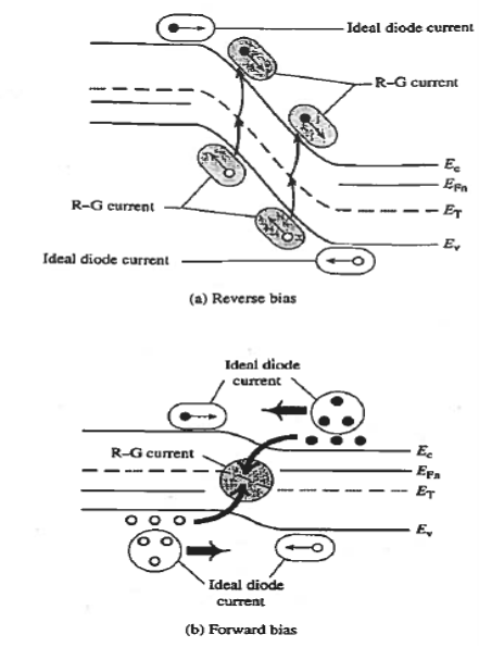
For the small forward biases and all the reverse biases at room temperature, a current beyond the predicted values from the ideal diode theory was observed. Such current is formed by the thermal carrier recombination-generation in the depletion region, but such R-G process is neglected in the ideal diode theory.
When the diode is reverse biased, however, the carrier concentrations in the depletion region are reduced below their equilibrium values leading to the thermal generation of electrons and holes throughout the region. The large electric field in the depletion region rapidly sweeps the generated carriers into the quasineutral regions, thereby adding to the reverse current. Forward biasing increases the carrier concentrations in the depletion region above their equilibrium values giving rise to carrier recombination in the region.
One can effectively view the resulting added forward current as arising from the carriers that cannot make it over the potential hill being partially eliminated via recombination at R-G centers in the depletion region.
To establish a quantitative expression for the added current, arising from thermal recombination-generation in the depletion region, we note that the net R-G rate is the same for electrons and holes under steady state conditions.
Moreover, for every electron-hole pair created or destroyed in the depletion region per second, one electron per second flows into or out of the diode contacts. Summing either the electrons or the holes created/destroyed throughout the depletion region per second and multiplying by q should therefore give the magnitude of the added current flowing in the device.
Thus current flowing in device is given as
 ……….(1)
|
Figure 20: R-G Current (a) Reverse biasing generation (b) forward biasing recombination in the depletion region
Note that, because of the conditions prevalent in the depletion region, the familiar special-case R-G relationship, |thermal R-G =-
 n is not applicable. Rather, the general-case result is applied
For reverse biases greater than a few kT/q. the carrier concentrations become quite small throughout most of the depletion region. Concentrations of carrier is negligible, n
Where
………..(5)
|
For forward biases the carrier concentrations cannot be neglected
We merely note that IR-G is expected to vary roughly as exp(qVA/ kT), 1<
 2, for forward biases greater than a few kT/q. Typically, the expected
  is close to 2, and the combined forward and reverse bias dependence is approximately described by
|
With the introduction of a second current component, it is common practice to refer to the current described by the ideal diode equation as the diffusion current, IDIFF. The diffusion current expression is rewritten here to facilitate a comparison of the two components:
|
The total current flowing in the diode is of course just the sum of the diffusion current and the R—G current:
 …………(8)
We concluded that
- In Si diodes at room temperature qAniW/2
 0 and the IR-G current dominates at reverse biases and small forward biases.
 - The reverse bias IR-G is proportional to W, the reverse current never saturates, but continually increases with increasing reverse bias.
- The forward bias IR-G varies as exp(qVA/
 kT) for VA > kT/q,
 - With increasing forward biases the IDIFF component, which increases more rapidly with voltage, eventually overtakes the IR-G component, leading to the q/kT region on a semilog plot of the forward-bias characteristics.
- IDIFF
 while IR-G
  the relative weight of the two components varies significantly from semiconductor to semiconductor.
 - The reverse bias diffusion component of the current will increase at a faster rate with increasing temperature.
SERIES RESISTANCE
The quasi neutral regions have an inherent resistance determined by the doping and dimensions of the regions. Although the value of resistance is quite small even in well-made devices but there is also a residual resistance associated with the diode contacts. These combine to form a resistance.
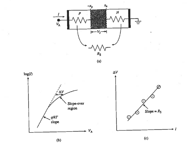
Rs in series with the current flow across the junction is shown in Figure 21(a). At low current levels the voltage drop across the series resistance. IRs, is totally negligible compared to the applied voltage drop across the depletion region better known as the "junction" voltage VJ.
Under the cited condition, VJ = VA, as assumed in the electrostatic and ideal diode derivations, At current levels where IRs becomes comparable to VA, however, the applied voltage drop appearing across the depletion region is reduced to
VJ = VA— IRs ……….(1)
Effectively, part of the applied voltage is wasted, a larger applied voltage is necessary to achieve the same level of current compared to the ideal
To correct for the series resistance, replace VA by VJ = VA— IRs
Since the diffusion current typically dominates at the current levels where IRs becomes important, we can write
|
Technically Eq. (2) is a transcendental equation that cannot be solved for I as a function of VA. However, I versus VA is readily established by choosing a VJ value, computing I from Eq. (2), and then computing VA from Eq. (1). The computation does require knowledge of Rs.
Rs can be determined by extending the ideal-diode part of the plot into the slope-over region and notes the  V voltage displacement between the two curves as a function of I Since
  V =VJ - VA= IRs , the slope of the line through a plot of the
  V versus I data yields Rs.
|
Figure 21: Identification and determination of the series resistance. (a) Physical origin of Rs. (b) Forward-bias semilog plot used to deduce  V versus I (c)
  V versus / plot used to deduce Rs.
HIGH-LEVEL INJECTION
To derive ideal diode equation we made the assumption of low-level injection but unfortunately it fail when the minority carrier concentration at the depletion region edge on the lightly doped side of the junction approaches the doping concentration.
In Si at room temperature this typically occurs at applied voltages a few tenths of a volt below Vbi . A further increase in the applied voltage gives rise to high-level injection.
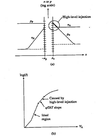
Under high-level injection both the minority carrier and the majority carrier concentrations adjacent to the depletion region are perturbed, as shown in Figure 22 (a).
|
Figure 22: High level injection (a) Carrier concentration under high-level injection condition (b) Predicted effect on the observed characteristics.
The majority carrier concentration must increase to maintain approximate charge neutrality in the quasineutral regions.
An analysis of high-level injection leads to a predicted current varying roughly as exp(q/2kT). In other words, one expects a high-current q/2kT region on a semilog plot of the forward bias I-V characteristics as sketched in Figure 22 (b). The predicted high-current q/2kT region is rarely observed.
The enhanced carrier concentrations associated with high-level injection can reduce the observed series resistance. The reduction in resistivity resulting from high levels of carrier injection is referred to as conductivity modulation.
Key Takeaways
- A moderately long list of assumptions was involved in deriving the ideal diode equation. Some of the assumptions were made without any a priori justification.
- The possible sources for the deviations from the ideal pn junction diodes can happen: Avalanching, Zener Process, The R-G current, Series Resistance, High-Level Injection
- R-G current: For the small forward biases and all the reverse biases at room temperature, a current beyond the predicted values from the ideal diode theory was observed. It is given by
|
- The diffusion current expression is given as
|
- The total current flowing in the diode is of course just the sum of the diffusion current and the R—G current:
|
- Series resistance: The quasi neutral regions have an inherent resistance determined by the doping and dimensions of the regions.
- The slope of the line through a plot of the
 V versus I data yields Rs.
 - High-Level Injection: increase in the applied voltage gives rise to high-level injection. Under high-level injection both the minority carrier and the majority carrier concentrations adjacent to the depletion region are perturbed
- The majority carrier concentration must increase to maintain approximate charge neutrality in the quasineutral regions.
- The reduction in resistivity resulting from high levels of carrier injection is referred to as conductivity modulation.
2.7 JUNCTION BREAKDOWN (AVALANCHE AND ZENER)
JUNCTION BREAKDOWN
Junction breakdown occurs when the large reverse current flows as the reverse voltage exceeds a certain value. it is a completely reversible process. Breakdown does not damage the diode but we still need to limit the current to avoid excessive heating.
The absolute value of the reverse voltage where the current goes off to infinity is known as the breakdown voltage and is given the symbol VBR, VBR tends to increase with the band gap of the semiconductor used to fabricate the diode.
The Avalanche Breakdown and Zener Breakdown are two different mechanisms by which a PN junction breaks. The Zener and Avalanche breakdown both occur in diode under reverse bias.
The avalanche breakdown occurs because of the ionisation of electrons and hole pairs whereas the Zener breakdown occurs because of heavy doping. These are explained below in details.
AVALANCHING
Consider a reverse biased diode, Voltage VA is applied as compared to the diode which is smaller than the breakdown voltage. We know that the reverse current is flowing in the diode is entirely due to the minority carriers.
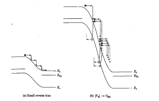
Minority carriers entering the depletion region and being accelerated by the electric field in the region to the other side of the junction. In crossing the depletion region the carrier acceleration is not continuous but is interrupted by energy-losing collisions with the semiconductor lattice, as shown in Figure 23(a).
Since the mean free path between collisions is 10-6 cm, and a median depletion width is 10-4 cm, a carrier can undergo tens to thousands of collisions in crossing the depletion region.
Thus at small applied reverse biases the energy lost by the carriers per collision is relatively small. The energy transferred to the lattice simply causes lattice vibrations there is just localized heating that is readily dissipated.
With increasing reverse bias the amount of energy transferred to the semiconductor lattice per collision systematically increases. Approaching the breakdown voltage, the energy transferred per collision becomes sufficient to ionize a semiconductor atom. By "ionize" we mean the collision frees a valence electron from the atom, or causes an electron from the valence band to jump into the conduction band, thereby creating an electron-hole pair. This phenomenon called impact ionization.
The added carriers created by impact ionization are immediately accelerated by the electric field in the depletion region. Consequently, they and the original carriers make additional collisions and create even more carriers as shown in Figure 23(b). At the breakdown voltage the carrier creation and reverse current effectively go off to infinity.
The Figure 23(b) energy band diagram is not and realistically could not be, drawn to scale. If the breakdown voltage were 100 V, for example, the distance between the p- and n-side Fermi levels would have to be approximately 100 times the Ec-Ev band gap distance. Second the avalanche breakdown does not occur sharply at VA = —VBR.
|
Figure 23: Avalanching
The increase in current associated with the carrier multiplication. For this purpose we will introduce multiplication factor, M. if I0 is the current before the multiplication of carriers then
 ………(1)
The value of M can be obtained from experimental fact as
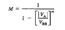 ………(2)
where power in the denominator m can have value between 3 and 6. m depends upon the type of semiconductor used in manufacturing the diode.
We next seek to explain the Veit dependence noted in the breakdown introduction. From the qualitative description of avalanching, it was concluded that
Breakdown occurs when the carriers gain an ionizing amount of energy in traveling a lattice-scattering mean free path. This should be true independent of the junction doping. A specific energy gain over a given distance, however, corresponds to a specific electric field. In other word.. breakdown occurs when the electric field in the depletion region reaches some critical value ξCR. essentially independent of the junction doping.
Considering a step junction, evaluating the electric field at x = 0, we find
Squaring the above expression we have
Since ξCR is independent of doping, the right-hand side of Eq. (4) must likewise be independent of doping. The right-hand side of Eq. (4) will be independent of doping if
or for asymmetrically doped junctions
|
The Eq. (6) is close enough to the experimental result. VBR increases with increase in temperature.
Lattice scattering increases with increase in temperature, Lattice scattering increases means a smaller mean free path, a larger critical electric field for avalanching, and hence a higher breakdown voltage.
ZENER
Zener Process is tunneling in a reverse-biased diode.
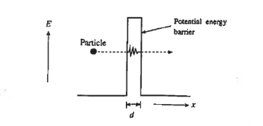
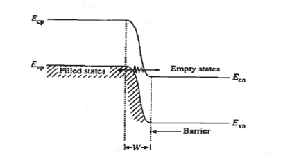
We already know that tunneling is quantum phenomena it does not have any classical analogy. As you can see in figure the tunnelling. Particle is travelling from left to right face a potential barrier. The height of the barrier is assumed to be greater than the kinetic energy of the particle.
Classically, the particle can cross this barrier after getting sufficient energy and go over the top of the barrier. However Quantum mechanically, there is another way the particle can cross the barrier. The process of particle moving through the potential barrier is known as Tunneling. The particle energy remains constant during the process.
Requirements for tunnelling to occur are given below:
(I) There must be filled states on one side of the barrier and empty states on the other side of the barrier at the same energy. Tunneling cannot take place into a region void of allowed states.
(2) The width of the potential energy barrier, d must be very thin. Quantum-mechanical tunneling becomes significant only if d < 100 Å = 10-6 cm.
|
Figure 24: Visualisation of tunnelling
Zener process is tunneling in a reverse-biased pn junction diode is shown in figure.
Tunneling takes place when the electrons from filled valence p side pass through the potential barrier (or depletion width) to empty states at the same energy in the conduction band on the n-side of the junction. The greater the reverse bias, the larger the number of filled valence-electron states on the p - side placed opposite empty conduction-band states on the n-side, and hence the greater the reverse-bias tunneling current.
For tunneling to be significant. the barrier thickness, roughly the depletion width in the case of the pn junction diode, must be <10 -6 cm.
Thus the Zener process is important only in diodes that are heavily doped on both sides of the junction. The breakdown voltage of the diodes is correspondingly small. The Zener process makes a significant contribution to the break- down current in diodes
|
Figure 25: Visualisation of tunnelling in reverse biased condition
Point of differences between avalanching and Zener process
- The VBR associated with avalanching increases with increasing temperature, VBR decreases with increasing T if the Zener process is dominant.
- The avalanche breakdown occurs in the thick region, whereas the Zener breakdown occurs in the thin region.
- After the avalanche breakdown, the junction of the diode will not regain its original position, whereas after the Zener breakdown the junction regains its original position.
- The existence of the electric field is more on the Zener breakdown as compared to the avalanche breakdown. Because the mechanism of Zener breakdown occurs in the heavily doped region.
- The avalanche breakdown produces the pairs of electrons and holes because of the thermal effects, whereas the Zener diode produces the electrons.
- The avalanche breakdown occurs in low doping material, whereas the Zener breakdown occurs in high doping material.
- The breakdown characteristics associated with the Zener process are very "soft. The current exhibits a very slow approach to infinity even when observed on a relatively coarse scale.
Key Takeaways
- Junction breakdown occurs when the large reverse current flows as the reverse voltage exceeds a certain value. it is a completely reversible process.
- Breakdown does not damage the diode but we still need to limit the current to avoid excessive heating.
- The absolute value of the reverse voltage where the current goes off to infinity is known as the breakdown voltage and is given the symbol VBR,
- VBR tends to increase with the band gap of the semiconductor used to fabricate the diode.
- The Avalanche Breakdown and Zener Breakdown are two different mechanisms by which a PN junction breaks.
- The Zener and Avalanche breakdown both occur in diode under reverse bias.
- The avalanche breakdown occurs because of the ionisation of electrons and hole pairs whereas the Zener breakdown occurs because of heavy doping. These are explained below in details.
- The avalanche breakdown occurs in low doping material, whereas the Zener breakdown occurs in high doping material.
2.8 REVERSE BIAS JUNCTION CAPACITANCE
We know that capacitance means the ability to store electric charge. A reverse biased p-n junction diode also stores electric charge at the depletion region just like the capacitors. There are immobile positive and negative ions in the depletion region.
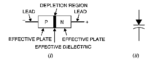
In a reverse biased p-n junction diode, the p-type and n-type regions have low resistance. Hence, p-type and n-type regions act like the electrodes or conducting plates of the capacitor. The depletion region of the p-n junction diode has high resistance and acts like the dielectric or insulating material. Thus, p-n junction diode can be considered as a parallel plate capacitor.
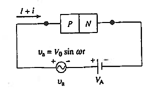
Figure 26: Diode biasing circuit
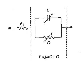
Figure 27: Equivalent pn diode circuit |
In depletion region, the electric charges (positive and negative ions) do not move from one place to another place. However, they exert electric field or electric force. Therefore, charge is stored at the depletion region in the form of electric field. The ability of a material to store electric charge is called capacitance. Thus, there exists a capacitance at the depletion region.
The capacitance at the depletion region changes with the change in applied voltage. When reverse bias voltage applied to the p-n junction diode is increased, a large number of holes (majority carriers) from p-side and electrons (majority carriers) from n-side are moved away from the p-n junction. As a result, the width of depletion region increases whereas the size of p-type and n-type regions (plates) decreases.
The p-n junction diode with narrow depletion width and large p-type and n-type regions will store large amount of electric charge whereas the p-n junction diode with wide depletion width and small p-type and n-type regions will store only a small amount of electric charge. Therefore, the capacitance of the reverse bias p-n junction diode decreases when voltage increases.
Pn junction diode differ from standard capacitance because diode capacitance monotonically decreases with increases reverse bias.
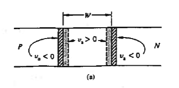
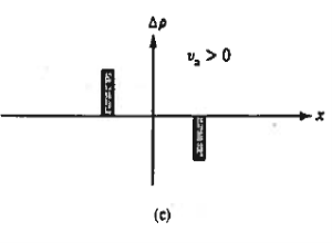
With the ac. signal superimposed on the d.c. bias, the total voltage drop across the junction becomes VA + va During the positive portion of the va, cycle, the a.c. signal slightly reduces the reverse bias across the junction, and the depletion width shrinks by a small amount as shown in Figure 28(a).
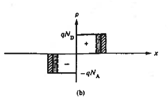
The ρ plot in Figure 28(b), shows that there is a decrease in the charge on the two sides of the depletion region.
When the a.c. signal reverses and goes negative. va, now increases the total reverse bias across the junction to greater than VA, and the depletion width increases slightly above its steady state value.
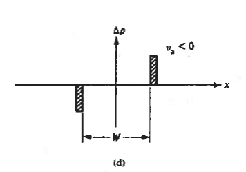
A depletion width larger than the steady state value in turn gives rise to an increase in the depletion region charge on the two sides of the junction. The overall effect of the a.c. signal may thus be viewed as a small oscillation of the depletion width about its steady state value and an associated  charge density oscillation, as pictured in Figure 28(c) and (d).
The p-plots were obtained by subtracting the d.c. charge density distribution in Fig. 7.4(b) from the VA ± va charge density distribution.
The diode capacitance is concluded

The capacitance associated with the depletion width oscillation is known as the junction or depletion-layer capacitance
|
Figure 28: Depletion layer charge considerations. (a) Depletion width (b) total charge density oscillates in response to an applied a.c. signal. (c) va > 0 and (d) va < 0 a.c. charge densities.
W increases with increasing reverse bias. CJ being proportional to 1/W is therefore expected to decrease with increased reverse biasing.
Key Takeaways
- A reverse biased p-n junction diode also stores electric charge at the depletion region just like the capacitors.
- There are immobile positive and negative ions in the depletion region.
- In a reverse biased p-n junction diode, the p-type and n-type regions have low resistance.The diode capacitance is concluded

- The capacitance associated with the depletion width oscillation is known as the junction or depletion-layer capacitance
- W increases with increasing reverse bias. CJ being proportional to 1/W is therefore expected to decrease with increased reverse biasing.
2.9 FORWARD BIAS DIFFUSION CAPACITANCE
Diffusion capacitance occurs in the forward biased PN junction. Here the diffusion capacitance has larger value than transition capacitance. Diffusion capacitance occurs due to stored charge of minority carriers near depletion region. The electrons(majority carriers) which cross the depletion region and enter into the p region will become the minority carriers of the p region. Similarly the holes which cross the depletion region and enter into the n region will become minority carriers of the n region. This large no of charge carriers accumulated near depletion region before they recombine. The accumulated charge on both side of the depletion region behaves like electrodes and the thin depletion region acts like dielectric.
|
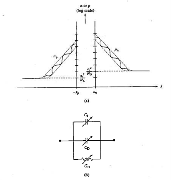
Figure 29: (a) Forward bias diffusion capacitance (Minority carrier charge fluctuation) (b) Equivalent diode biasing circuit
Charge oscillations inside of a device structure generate Capacitance. We studied that when diode is reverse biased there is in-and-out movement of majority carriers about the steady state depletion width is responsible for Junction capacitance. However when a.c. signal is applied minority carriers also oscillate about the edges of the depletion width, but as we know minority carriers are less in number so there contribution to the admittance is negligible.
Now we will see the case of forward biasing the diode. When diode is forward biased the majority carriers response similar as discussed previous nothing new is added. These carriers still move back and forth about the edges of the depletion region giving rise to a junction capacitance.
Under forward bias minority carrier charge oscillation in response to the a.c. signal contribute significantly.
Forward biasing of the diode causes a accumulation of minority carriers in the quasineutral regions immediately adjacent to the depletion region. The accumulation becomes larger and larger with increasing forward bias. In response to an a.c. signal, the voltage drop across the junction is changed to VA + va, and the excess minority carrier distributions oscillate about their d.c. values as shown in Figure 29(a). This results in an additional capacitance.
If the minority carriers can follow the signal quasistatically, the carriers move back and forth in unison between the two straight lines in the figure. However, the supply and removal of minority carriers is not as rapid as that of the majority carriers.
As the angular frequencies approaching the inverse of the minority carrier lifetimes, the minority carrier charge oscillation has difficulty staying in sync with the an. signal. The result is an out-of-phase spatial variation of the charge something like the undulating distributions as shown in Figure 29(a). An out-of-phase charge oscillation enhances the observed conductance and reduces the observed capacitance.
In other words, the capacitance and conductance associated with the minority carrier oscillations are expected to be frequency-dependent. Because the minority carrier build-up about the edges of the depletion region is caused by the diffusion current, the admittance associated with the minority carrier charge oscillation is called the diffusion admittance, YD given as
YD = GD + ωjCD
where CD and GD are the diffusion capacitance and diffusion conductance, respectively.
Key Takeaways
- Diffusion capacitance occurs in the forward biased PN junction.
- Here the diffusion capacitance has larger value than transition capacitance. Diffusion capacitance occurs due to stored charge of minority carriers near depletion region.
- The accumulated charge on both side of the depletion region behaves like electrodes and the thin depletion region acts like dielectric.
- The capacitance and conductance associated with the minority carrier oscillations are expected to be frequency-dependent.
- Diffusion admittance, YD given as
YD = GD + ωjCD
- where CD and GD are the diffusion capacitance and diffusion conductance, respectively.
2.10 QUALITATIVE UNDERSTANDING OF TURN ON AND TURN-OFF TRANSIENTS
When the pn junction diode is in forward bias condition it is termed as on state and When the diode is in reverse bias condition it is termed as off state. When the diode is in forward bias condition a relatively large current can be produced by a small applied voltage whereas in reverse bias only a very small current will flow. Thus pn junction diode can be used as an electrical switch in many applications.
The speed of the pn junction diode in switching states is matter in the applications. We will qualitatively discuss the transients that occur and the charge storage effects.
The Turn-off Transient
In the turn-off transient there is a delay in going from the on-state to the off-state. The root cause of the delay in switching between the on and off states is easy to identify. As discussed forward biasing of the diode, causes a build-up or storage of excess minority carriers in the quasineutral regions immediately adjacent to the depletion region. When the diode is reverse biased, on the other hand, there is a deficit of minority carriers in the near-vicinity of the depletion region.
Going from the on-state to the off-state, the excess minority carriers must be removed from the two sides of the junction. The storage delay time derives its name from the fact that the majority of the stored charge is being removed from the diode during the transient.
Removal of the excess minority carrier charge in the quasineutral regions can be achieved in two ways. For one, the carriers can be eliminated in place via recombination. Recombination is of course not instantaneous; several minority carrier lifetimes would be required to go from the on-state to the off-state if recombination were the sole means of carrier removal. The other method of reducing the carrier excess is by net carrier flow out of the region
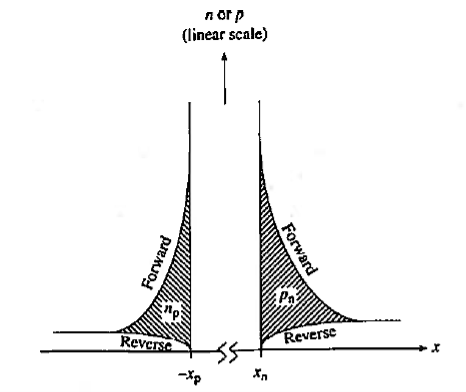
Suppose we want to switch a diode from the forward bias on state to the reverse-bias off state. There is excess minority carrier charge stored in both the p and n regions of the diode. The excess minority carrier concentrations at the space charge edges are supported by the forward-bias junction voltage. When the voltage is switched from the forward- to the reverse-bias state, the excess minority carrier concentrations at the space charge edges can no longer be supported and they start to decrease, as shown in Figure.
But the junction capacitances do not allow the junction voltage to change instantaneously. After storage time, the voltage across the junction will begin to change.
When a pn junction is switched from forward bias to reverse bias, the stored excess minority carrier charge must be removed from the junction. The time required to remove this charge is called the storage time and is a limiting factor in the switching speed of a diode. If the minority carriers are removed at fast then the diode turns of rapidly. So to switch the diode quickly, we need to be able to produce a large reverse current as well as have a small minority carrier lifetime. In the design of diode circuit then, the designer must provide a path for the transient reverse-bias current pulse in order to be able to switch the diode quickly.
|
Figure 30: Turn on and Turn-off transients
The figure shows stored minority carrier charge leading to the delay in switching between the on and off states. The reverse and forward minority carrier concentration is plotted simultaneously on a linear scale with the x coordinates matched at the depletion region edges. The break in the x-axis inside the depletion region acknowledges a difference in the forward-bias and reverse-bias depletion widths. The cross-hatched areas identify minority carriers that must be removed far switching to be complete.
The Turn-on Transient
The turn-on transient occurs when the diode is switched from its "off" state into the forward-bias "on" stale. The turn-on can be accomplished by applying a forward-bias current pulse. The process is completed in two stages.
The first stage of turn-on occurs very quickly and is the length of time required to narrow the space charge width from the reverse-bias value to its thermal-equilibrium value. During this time, ionized donors and acceptors are neutralized as the space charge width narrows.
The second stage of the turn-on process is the time required to establish the minority-carrier distributions. During this time the voltage across the junction is increasing toward its steady-state value.
A small turn-on time is achieved if the minority carrier lifetime is small and if the forward-bias current is small.
Key Takeaways
- In the turn-off transient there is a delay in going from the on-state to the off-state.
- Going from the on-state to the off-state, the excess minority carriers must be removed from the two sides of the junction.
- The turn-on transient occurs when the diode is switched from its "off" state into the forward-bias "on" stale.
- The turn-on can be accomplished by applying a forward-bias current pulse. The process is completed in two stages.
- A small turn-on time is achieved if the minority carrier lifetime is small and if the forward-bias current is small.
The satisfactory explanation of this breakdown of the junction was first given by the American scientist C. Zener. A zener diode is a special type of diode that is designed to operate in the reverse breakdown region.
An ordinary diode operated in this region will usually be destroyed due to excessive current. This is not the case for the zener diode.
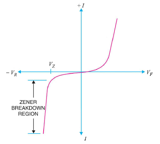
It has already been discussed that when the reverse bias on a crystal diode is increased, a critical voltage, called breakdown voltage is reached where the reverse current increases sharply to a high value. The breakdown region is the knee of the reverse characteristic as shown in Figure 32.
The breakdown voltage is sometimes called zener voltage and the sudden increase in current is known as zener current.
The breakdown or zener voltage depends upon the amount of doping. If the diode is heavily doped, depletion layer will be thin and consequently the breakdown of the junction will occur at a lower reverse voltage.
On the other hand, a lightly doped diode has a higher breakdown voltage. When an ordinary crystal diode is properly doped so that it has a sharp breakdown voltage, it is called a zener diode. A properly doped crystal diode which has a sharp breakdown voltage is known as a zener diode.
Figure 31 shows the symbol of a zener diode. It may be seen that it is just like an ordinal, diode except that the bar is turned into z-shape.
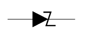
Figure 31: Symbol of a zener diode
|
Figure 32: I-V characteristics of zener diode
As the curve reveals, two things happen when Vz is reached:
- The diode current increases rapidly.
- The reverse voltage Vz across the diode remains almost constant.
The following points may be noted
(i) A zener diode is like an ordinary diode except that it is properly doped so as to have a sharp breakdown voltage.
(ii) A zener diode is always reverse connected i.e. it is always reverse biased.
(iii) A zener diode has sharp breakdown voltage, called zener voltage Vz.
(iv) When forward biased, its characteristics are just those of ordinary PN junction diode.
(v) The zener diode is not immediately burnt just because it has entered the breakdown region. As long as the external circuit connected to the diode limits the diode current to less than burn out value, the diode will not burn out.
In other words, the zener diode operated in this region will have a relatively constant voltage across it, regardless of the value of current through the device. This permits the zener diode to be used as a voltage regulator or voltage stabiliser.
Key Takeaways
- A zener diode is a special type of diode that is designed to operate in the reverse breakdown region.
- The breakdown region is the knee of the reverse characteristic
- The breakdown voltage is sometimes called zener voltage and the sudden increase in current is known as zener current.
- The breakdown or zener voltage depends upon the amount of doping.
- Because of its special characteristics zener diode used as voltage stabiliser
Tunnel diode is a type of heavily doped semiconductor that exhibits negative resistance (i.e. current decreases as the voltage is increased) in certain regions in the forward direction. The symbol of tunnel diode is given below

Figure 33: Symbol of tunnel diode
We can also define it as “A tunnel diode is a pn junction that exhibits negative resistance between two values of forward voltage (i.e., between peak-point voltage and valley-point voltage)”.
We know that a conventional diode exhibits "positive resistance when it is forward biased or reverse biased but this is not happening in tunnel diode.
The tunnel diode is basically a pn junction with heavy doping of p-type and n-type semiconductor materials. Doping in a tunnel diode is approximately 1000 times as heavily as a conventional diode. This heavy doping results in a large number of majority carriers. Because of the large number of carriers, most are not used during the initial recombination that produces the depletion layer. As a result, the depletion layer is very narrow. In comparison with conventional diode, the depletion layer of a tunnel diode is 100 times narrower.
Working of tunnel diode includes the quantum tunneling effect and that’s why it is named as tunnel diode. Let us recall the tunnelling effect.
Tunneling effect: There are large numbers of majority carriers because of the heavy doping. These carriers drift in p and n sections.
Many valence electrons raised their energy level closer to the conduction region because of the drift activity. The movement of valence electrons from the valence energy band to the conduction band with little or no applied forward voltage is called tunneling. Valence electrons seem to tunnel through the forbidden energy band.
As we increase the forward voltage, current in the diode rises initially due to tunneling effect. But on further increasing of forward voltage the tunneling effect is reduced and current flow starts to decrease. Thus tunnel diode is said to have entered the negative resistance region. As the voltage is further increased the tunneling effect plays less and less part until a valley-point is reached. From now onwards, the tunnel diode behaves as ordinary diode i.e., diode current increases with the increase in forward voltage.
V-I Characteristic
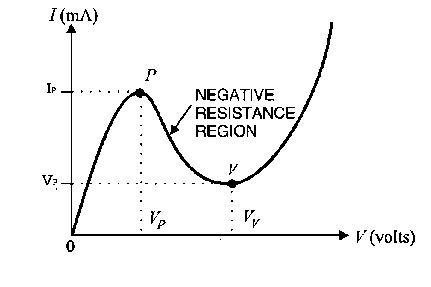
- Electrons from the n-region "tunnel" through the potential barrier to the p-region as the forward voltage across the tunnel diode is increased from zero. As the forward voltage increases, the diode current also increases until the peak-point P is reached. The diode current has now reached peak current Ip at about peak-point voltage Vp. The diode has exhibited positive resistance.
- As the voltage is increased beyond VP, the tunneling action starts decreasing and the diode current decreases as the forward voltage is increased until 'valley-point VV is reached. In the region between peak-point and valley-point (i.e.. between points P and V), the diode exhibits negative resistance i.e., as the forward bias is increased, the current decreases. This suggests that tunnel diode, when operated in the negative resistance region, can be used as an oscillator or a switch.
|
Figure 34: V-I Characteristic
- When forward bias is increased beyond valley-point voltage Vv the tunnel diode behaves as a normal diode. In other words, from point V onwards, the diode current increases with the increase in forward voltage i.e., the diode exhibits positive resistance once again.
Key Takeaways
- Tunnel diode is a type of heavily doped semiconductor that exhibits negative resistance (i.e. current decreases as the voltage is increased) in certain regions in the forward direction.
- A tunnel diode is a pn junction that exhibits negative resistance between two values of forward voltage.
- Doping in a tunnel diode is approximately 1000 times as heavily as a conventional diode.
- In comparison with conventional diode, the depletion layer of a tunnel diode is 100 times narrower.
- Working of tunnel diode includes the quantum tunneling effect and that’s why it is named as tunnel diode. Let us recall the tunnelling effect
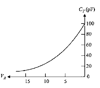
A junction diode which acts as a variable capacitor under changing reverse bias is known as a varactor diode.
We already studied that depletion layer is formed when p and n type material form pn junction diode. If there are no charge carriers within the depletion region, depletion region acts as an insulator.
The p-type material with holes as majority carriers and n-type material with elections as majority carriers act as charged plates. Thus the diode may be considered as a capacitor with n-region and p-region forming oppositely charged plates and with depletion region between them acting as a dielectric. Varactor diode is specially constructed to have high capacitance under reverse bias. The values of capacitance of varactor diodes are in the picofarad (1012 F) range.
|
Figure 35: (i) Varactor diode (ii) Shows the symbol of varactor diode
A varactor diode is always reverse biased. The capacitance of varactor diode is given as:

Where CT = Total capacitance of the junction
Ɛ = Permittivity of the semiconductor material
A = Cross-sectional area of the junction
Wd= Width of the depletion layer
When reverse voltage across a varactor diode is increased, the width Wd of the depletion layer increases. Therefore, the total junction capacitance CT of the junction decreases.
On the other hand, if the reverse voltage across the diode is decreased, the width Wd of the depletion layer decreases. Consequently, the total junction capacitance CT increases.
|
Figure 36: Shows the variation of VR and CT
Figure shows the variation of reverse bias varactor voltage VR and total junction capacitance CT. By changing varactor voltage VR we can easily change junction capacitance CT that is why varactor is also known as Voltage controlled capacitor.
Key Takeaways
- A junction diode which acts as a variable capacitor under changing reverse bias is known as a varactor diode.
- If there are no charge carriers within the depletion region, depletion region acts as an insulator.
- Varactor diode is specially constructed to have high capacitance under reverse bias. The values of capacitance of varactor diodes are in the picofarad (1012 F) range.
- The capacitance of varactor diode is given as:

A scientist named Walter.H.Schottky first discovered Schottky diode. A Shockley diode is a PNPN device having two terminals. This device consists of four alternate P-type and N-type layers in a single crystal and acts as a switch. The various layers are labelled as P1, N1, P2, and N2 for identification.
Since a P-region adjacent to an N-region may be considered a junction diode, the Shockley diode is equivalent to three junction diodes connected in series as shown in Figure 37 (ii). The symbol of Shockley diode is shown in Figure 37 (iii).
|
Figure 37: (i) Shockley diode (ii) equivalent figure to Shockley diode (iii)The symbol of Shockley diode
Schottky diode is a device, which comes under the type of a metal semiconductor junction diode. Barrier diode and low voltage diodes are the other names for Schottky diode. When compared to a PN junction diode, power drop is lower in Schottky diode.
Working
When we forward biased the Shockley diode i.e., making anode is more positive w.r.t. cathode, as a result diodes D1 and D3 would be forward-biased while diode D2 would be reverse-biased. Since diode D2 offers very high resistance and the three diodes are in series, the Shockley diode presents a very high resistance. As the forward voltage increases, the reverse bias across D2 is also increased.
If we keep on increasing forward biasing a point reached when voltage become break over voltage VBO, reverse breakdown of D2 occurs. Since this breakdown results in reduced resistance, the Shockley diode presents a very low resistance. From now onwards, the Shockley diode behaves as a conventional forward-biased diode; the forward current being determined by the applied voltage and external load resistance.
|
Figure 38: V-I characteristic
When Shockley diode is reverse biased (i.e., anode is negative w. rt. cathode), diodes D1 and D3 would be reverse-biased while diode D2 would be forward-biased. If reverse voltage is increased sufficiently, the reverse voltage breakdown (point A in Figure 36) of Shockley diode is reached. At this point, diodes D1 and D3 would go into reverse-voltage breakdown, the reverse current flowing through them would rise rapidly and the heat produced by this current flow could ruin the entire device. For this reason, Shockley diode should never be operated with a reverse voltage sufficient to reach the reverse-voltage breakdown point.
Shockley diode behaves like a switch. So long as the forward voltage is less than break over voltage, Shockley diode offers very high resistance (i.e. switch is open) and practically conducts no current. At voltages above the break-over value, Shockley diode presents a very low resistance (i.e. switch is closed) and Shockley diode conducts heavily.
It may be noted that Shockley diode is also known as PNPN diode or four layer diode or reverse-blocking diode thyristor.
Once Shockley diode is turned ON (i.e., it starts conducting), the only way to turn it OFF is to reduce the applied voltage to such a value so that current flowing through Shockley diode drops below its holding current IH value. Diode D2 then comes out of its reverse-breakdown state and its high-resistance value is restored. This, in turn, causes the entire Shockley diode to revert to its high-resistance (switch open) state.
Key Takeaways
- A Shockley diode is a PNPN device having two terminals.
- Shockley diode behaves like a switch.
- It may be noted that Shockley diode is also known as PNPN diode or four layer diode or reverse-blocking diode thyristor.
- Once Shockley diode is turned ON (i.e., it starts conducting), the only way to turn it OFF is to reduce the applied voltage to such a value so that current flowing through Shockley diode drops below its holding current IH value.
References
- Semiconductor Device Fundamentals by Robert F. Pierret
- Physics of Semiconductor Devices by S.M. Sze.
- Principle of electronics S. Chand V K Mehta and Rohit Mehta
