Unit – 1
Introduction to Electronics
- Electronics vegan with invention of vacuum diode by J.A Fleming in 1897 and after that vacuum triode invented by lee de forest to amplify the signals.
- The Transistor Era began with the junction transistor invention in1948.from 1958 to 1975. integrated circuits (Ic’s) introduced which is a small signal chip such as small scale & very large scale integration .
- . Integrated circuits drastically changed the entire electronics natures as entire electronic circuit of integrated in a signal chip which has low cost ,small size, light in weight& more reliable.
- . The Use Off Germanium and silicon semiconductor materials made these transistor gain the popularity & widely used in deferent electronics circuits & devise.
- Inventions/ Discovery
1) 1720 Stephen Gray Discover edinsalator& conductor
2) 1745 Ewald Georg Von Kleist & Pieter Van Musschenbroetinvenredleyden jars(First Capacitor)
3) 1826 Georg Ohm Introduced OHM'S law
4) 1831 Reverend Nichols calland invented the inductor coil.
5) 1836 Nicholas Callan Invented Transformer
6) 1876 Alexander Graham Bell Invented Telephone
7) 1888 Heinrich Hertz proved that electromagnetic waves (FM) Travel over same distance.
8) 1897 Karl Ferdinand Braun Invented Cathode ray Oscilloscope (cro)
9)1901 Gaglielmo Marconi made First Transatlantic Radio broadcast
10) 1904 John Ambrose Fleming Invested diode
11) 1906 Leede forest invented triodes
12) 1912 Edwin Howard Armstrong develop electronic Oscillator.
13) 1920 Otis Frank Boykin invented resistor.
14) 1928 First Ereperimental television Broadcast in the us
15) 1929 First public TV Broadcast in Germany
16)1941 Konradzusc developed the first programmable computer
17)1943 Eisler invested the printed ckt board (BCB)
18)1944 John logic baird developed the first color picture tube.
19) 1947 First transistor at bell labor atonics by William Shockley, john Bardeen & welter Britain.
20) 1958 Jack Kirby invested the integrated circuit (IC)
21) 1960 Theodore Harold mailman invented the laser
22) 1962 Holstein & Heisman invented misfit transistors.
23) 1962 Nick Holon yak jr Invented the LED.
24) 1970 Intel Introduced the first Micro processor.
25) 1973 John F.Mitchell & Dr Martin cooper of Motorola invented the first mobile phone.
26) 2007 Apple introduced the first I phone.
Electronics engineering Field Have become an important part of human being. starting with an electronic alarm to get up early in the morning ,watch to update current news , microwave oven is used to cook the food , washing machine is used to clean our clothes 7 for entertainment music system is used. Now a days electronics devices every where is utilized such as in schools, colleges , homes, shops, health care, defense ,industries ,research, geographic, animation, etc
- The electronics industry is growing very fast & is creating good job opportunity in industries like mobile phone, IT Industries television ,computers ,laptops ,tablets ,& palmtops.
- In Addition to this there are good carrier options in consumer durables, oil, gas chemical &power electronics.
- In has many Applications ranging from healthcare satellite communication, mobile communication (2G,3G,& 4G) & Internet technology.
- Engineers with Bachelor of Electronics & Telecommunication can work in research , design & development & manufacturing of electronics applications.
- They also have job openings in sale & marketing of electronic Equipment& maintaining & repairing of electronic devices.
- It has various field such as VLSI Design .Microwave Engineering Integrated CKT .embedded system Nanotechnology , microelectronics & artificial intelligence soon.
Applications:-
1) Digital Commerce
ii) Mobile Phone
iii)Computers
iv)medical applications such as CT scan 1MRI
V) led traffic lights
vi) Led displays etc
An Electronic components is any basic discrete device or physical entity to affect electronics system used to affect electronics of their associated fields.
|
1) Components which requires 1) Components which do not require |
extremely source to their opr is extremely source to their opr is called |
called Active Components Passive Components |
2) If we Connect a diode in a circuit 2) If we connect a resistor to the supply |
And then connect this circuit to the vtg ,it starts work automatically without |
the supply vtg then diode will not using a specific voltage. |
Conduct the current until the supply |
vtg reach to 0.3 v(Ge) or 0.7 v(Si). |
3)Active component are able to inject 3) Passive component are not able to |
power to the ckt and control the energy amplify oscillation, modulation etc.do no |
. have bias vtg of trigger vtg and linear in Nature. |
4)Example: vtg source, current source 4) Resister , Capacitor, inductor, |
transistor, OPAMP,SC& etc. transformer |
5)Active components are able to 5)Passive components are consume the |
Provide the energy or power gain. Energy. It will not provide the power gain |

N type Semiconductor:-
To increase the number of conduction band electrons inintrisic silicon , pentavalent imparity atoms are added. these are atoms with five valence electrons such as
i) arsenic (as)
ii) phosphors (p)
iii) Bismuth (Bi)
iii) Antimony ( sb)
|
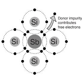
- Pentavalent impurity atom in a silicon crystal. an antimony (sb) impurity atom shown above-
- Each pentavalent atom forms covalent bonds with four adjustment silicon atoms, leaving one extra electron .
- The pentavalent atom gives up on electron , it often called a donor atom.
- Majority and minority carriers:- A type here means negative charge of an electron .electron are called the majority carriers in n-type material.
- Hole in an n-type material are called minority carriers
P Type Semiconductor :-
To increase the number of holes in intrinsic silicon trivalent impurity atoms are added these are atoms with there valence electrons such as
i) Baron(B)
ii) Indium(IN)
iii)Gallium(GO)
|
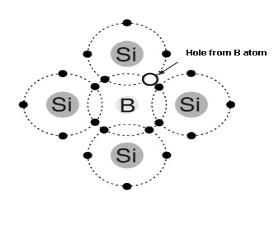
- Trivalent impurity atom in a silicon crystal structure . A) boron (B) impurity atom is shown in the center.
- The number of holes can be carefully controlled by the number of trivalent impurity atoms added to the silicon .
- A Hole created by the doping process is not accompanied by a conduction (free) electron.
- Trivalent Atom can take an electron it is often referred to as on accepted atom
Drift current :- When a vtg is applied to a semiconductor, the free electrons try to drift toward the positive terminal of the battery due to this current flow called drift current.
Diffusion current : In semiconductor it is possible to have a non uniform concentration of charge partials due to non uniform doping
eg. the concentration of e- on one side of the surface is more than the density on the other side , so the e- will move from the side of greater concentration to the side of lower concentration. this transport of result in to a flow of current which is called diffused current.
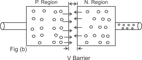
V Barrier
|
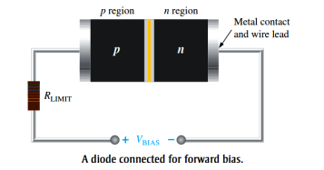
- A Forward biased showing the flow of majority carriers and the voltage due to the barrier potential across the depletion region-
- To bias a diode apply d,c vtg across it .
- Forward bias is the condition that allows current through the PN junction.
- Negative side of VBIAS is connected to the N -region of the diode and the positive side is connected to the P- region.
- A selected requirement is that the bias voltage VBIAS must be greater than the barrier potential.
- Because of like charges repel ,the negative side of the bias voltage source pushes the free electrons , which are the majority carriers in the N-region towards the PN junction .the flow of free is called Electron Current.
- The –Ve side of the source also provide a continues flow of electrons through the external connection (conductor).
- into the N-region as show in fig-B
- The bias voltage source imparts sufficient energy to the free electrons for them to overcome the barrier potential of the depletion region and move on through into the 'p' region once in the P-region .these conduction electrons have lost enough energy to immediately combine with holes in the valence band.
- Now the e- are in the valance band in the P-region simply because they have lost too much energy overcoming the barrier potential to remain in the conduction band. since unlike charge attract, the positive side of the bias voltage source attracts the valence electrons toward the left end of the region.
- The hole in the P-region provide the medium or "Pathway" for these valence electrons to move through the P-region.
- The holes which are the majority carriers in the P-region , effectively (not actually ) move to the right toward the junction as shown in fig-B.
- The defective flow of holes is called the hole current.
- As from Fig-B hole current as the flow of valence electrons through the P-region with the holes providing the only means for these electrons to flow.
- As the electrons flow out of the P-region through the external connection and to the positive side of the bias in the P-region at the same time these electrons become conduction electrons in the mater conductor .
- To these is a continues availability of holes effectively moving towards the PN junction stream of electrons as they come across the junction in to the P-region.
The effect of forward bias on the depletion region:-
|
Depletion Region
- Forward bias narrows the depletion region & produce a vtg drop across pn junction equal to the barrier potential.
- As more electrons flow into the depletion region , the number of positive ions is reduce . as more notes effectively flow into the depletion region on the other side of the pn junction ,the number of -ve ions is reduce this reduction in positive & -ve ions during forward bias causes the depletion region to narrow.
The Effect of the Barrier Potential during forward bias:-
- The electronic field between the positive and negative ions in the depletion region on either side of the junction creates an energy bill, that prevent free R form diffusing across the junction at equilibrium this is known as the barrier potential
- When forward bias is applied the free electrons are provided with enough energy from the bias voltage source to over come the barrier potential and effectively climb the energy bill and cross the depletion region.
- The energy that the electronics repair in order to pass through the depletion region is equal to the barrier potential.
- Electron gives up an amount of energy equivalent to the barrier potential when they cross the depletion region.
- This energy loss results in a vtg drop across the pn junction equals to the barrier potential (0.7v)
- An additional small vtg drop across the P & N regions due to the internal resistance of the material.
- For doped Semiconductor material ,this resistance called the dynamic resistance is very small and can usually be neglected.
REVERSE BIAS:-
Reverse bias is the condition the essentially prevents current through the diode.
P-region N- region
- +
|


V BIAS
A Diode connected for Reverse Biased-
- Because unlike charges attract the positive side of the bia voltage source pulls the free election , which are the majority carriers in the N-region away from the PN junction.
- AS the election flow towards the positive side of the voltage source additional positive ions are created
- This results in a widening of the depletion region and a depletion of majority carriers.
|


- The diode during the short transition time immediately after reverse bias vtg is applied-
- In the P-region electrons from the negative side of the vtg source enter as valence electron and move from hole to hole toward the depletion region where the creators additional -ve ions.
- This results in a widening of the depletion region and a depletion of majority carriers
- As the depletion region widens the availability of majority carriers decreases
- As more of the N & P regions become depleted of majority carriers ,the electric field between the positive and -ve ions increase in strength the depletion region equals the bios vtg .this point the transition current essentially ceases except for a small reverse current that can usually be neglected.
Reverse Current
- extremely small current that exist in reverse bias after the transition current dies act is caused by the minority carrier in the N& P region that are produced by the manly generated e hole pairs.
- The conduction band in the P-region is at a higher energy level then the conduction band in the N-region . therefore the minority easily pass through the depletion region because they required no additional energy.
|
The Extremely small reverse current in a reverse biased diode is due to the minority carriers from thermally generated
e=hole pairs
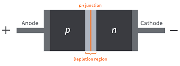
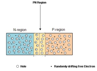
The Diode - Before doping the p-type & N-type consisting silicon material atom acting as a neutral.
IF a piece of intrinsic silicon is doped so that part is n-type and the other part is p-type , a junction forms at the bounded between the two regions and a diode is created.
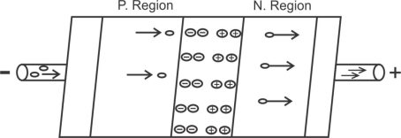
Formation of the Depletion Region
|
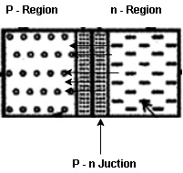
- At the instant of junction formation , free electrons in the N-region near the p-n junction being to diffuse across the junction and fall into holes near the junction in the P-region.
|
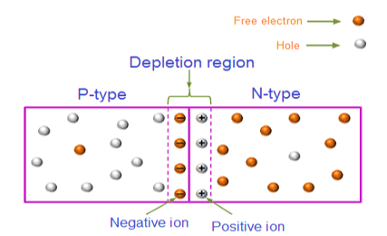
For every electron that defuse across the junction and combines with a hole , a positive charge is left in the region and a ve charge is created in the p-region firming a barriers potential. this action continues until the vtg of the barrier ripples further diffusion .
The Depletion region acts as a barriers to the farther movement of electrons across the junction
As positive ion & -ve ion across the junction produces a electric field across the junction -according to coulombs law.
The potential difference of the electric field across the depletion region is the amount of vtg required to move electronics through the electric field, this potential difference is called the barrier potential & is expressed in volt
The typical barrier potential is approximately 0.7 v for silicon & 0.3 v for germanium at 25c.
Whenever a specified voltage is exceeded, the diode resistance gets increased, making the diode reverse biased and it acts as an open switch. Whenever the voltage applied is below the reference voltage, the diode resistance gets decreased, making the diode forward biased, and it acts as a closed switch.
The following circuit explains the diode acting as a switch.
|
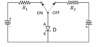
A switching diode has a PN junction in which P-region is lightly doped and N-region is heavily doped. The above circuit symbolizes that the diode gets ON when positive voltage forward biases the diode and it gets OFF when negative voltage reverse biases the diode.
As the forward current flows till then, with a sudden reverse voltage, the reverse current flows for an instance rather than getting switched OFF immediately. The higher the leakage current, the greater the loss. The flow of reverse current when diode is reverse biased suddenly, may sometimes create few oscillations, called as RINGING.
This ringing condition is a loss and hence should be minimized. To do this, the switching times of the diode should be understood.
1)Due to the unidirectional current flow through the transformer there is a possibility of core saturation to avoid this transformer size must be increased.
2)Ripple factor is high.
3)Low rectification effecting.
4)Law TUF.
5)Law D.C O/P VTG & current.
6)Large filter component are required.
ADVANTAGES:-
1)Simple Construction.
2) Component required less.
3)Small size.
APPLICATION:-
Walkman, law cost power supply.
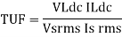
TRANSFORMER UTILISATION FACTOR(TUF) :-It indicates how well the ilp transformer is being utilized
TUF= DC O/P Power / AC power rating of the transformer
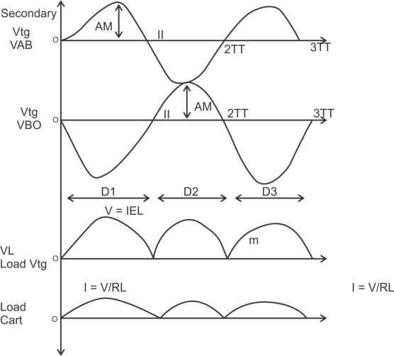
1)A center tapped rectifier is a type of full wave rectifier that uses two diode connected to the secondary of a center tapped transformer.
|
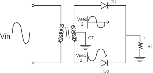
Center tapped full wave rectifier operation:-
I) During positive half cycle of i/p ac supply. diagram
D1.Is in forward biased & D2 is in reverse biased. II)During -ve half cycle.
D1 Reverse biased D2 Forward biased
|
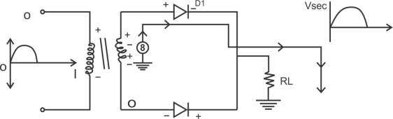
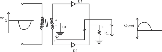
ADVANTAGES
1) law ripple factor as Compared to HKR.
2)Better rectification efficiency.
3) Better TUF.
4)Higher value of average load vtg & avg load crt.
5)No possibility of transformer core saturation.
DISADVANTAGES
PIV of diode is 2vm , more size costly.
APPLICATION
I) Battery charges.
2)power supply at laboratory, high current, electronic ckt.
BRIDGE RECTIFIER
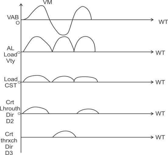
The bridge rectifier uses four diode connected, when the i/p cycle is positive diode D1 & D2 are forward biased and conduct current in the direction shown a vtg is developed across RL which looks the positive half of the i/p cycle during this diodes D3 and D4 are reverse biased.
When the ilp cycle is -ve diode D3& D4 are forward biased & conduct current in the same direction through R1 as during in the positive half cycle during the -ve half cycle D1& D2 are reverse biased. a full wave rectified O/P VTG appears across RL as a result of this action.
- during positive half cycle of ilp D1 & D2 are forward biased conduct current D3 & D4 are reverse biased:-
- during -ve half cycle of the ilp D3 &D4 are forward biased & conduct current D1 & D2 are reverse biased-
|
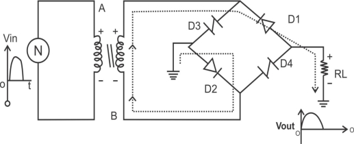
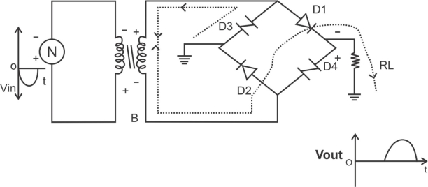
NOTE - Practically vp(out)= vp sec-1.4v 1000 diode knee vtg.
|
Advantages :-
1) It require a small size transformer center tap transformer is not required .this makes the bridge rectifier cost effective.
2) This ckt is most suitable for the high vtg application . this is because the max -ve that appears across each diode is -vm therefore the diode with PIV rating of -vm volts are required to be selected (PIV in fall wave rectifier is 2vm
3) Core saturation does not take place.
4) High TUF, high avg, vtg
Disadvantages :-
1)Number of diode used is four instead two for FWR
2)As two diodes conduct simultaneously , the vtg drop increase and the o/p vtg reduces.
Applications :-
Laboratory , high current, battery , electronic , ckt power supply.
- Zenor diode is a special type of p-n junction semiconductor diode in this diode the reverse breakdown voltage is adjusted precisely between 3v to 200v.
- Its applications are based on this principle hence zenor diode is called as a breakdown diode.
- The doping level of the imparity added to manufacture the zener diode is controlled in order to adjust the precise value of breakdown voltage.
PRINCIPLE OF OPERATION:- A zener diode can be forward biased or reverses biased. its operation in the forward biased mode is same as that of a p-n junction diode but its operation in the reverse biased mode is sustainably deferent.
|
An LED emits light when electrical energy is applied to it. for proper operation it is necessary to forward bias the LED.
Construction of LED :-
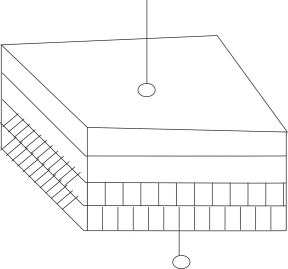
To make emission of light in one direction cup type construction is used For LED.
|
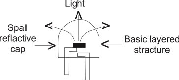
PRINCIPLE LED OPERATION
When the led is forward is forward biased the electrons in the n-region will cross the junction and recombine with the holes in the p- type material.
These free e- reside in the conduction band & hence at a higher energy level than the holes in the valence band
When recombination takes place this e- return peak to the valence band which is at a lower energy level than the conduction band.
while returning back the recombining e-give away the excess energy in the form of light . this process is called as electroluminescence. in this way an LED emits light.
Color of the Emitted Light
Material Use Color of Emitted Light
i)Gallium Arsenide (GOAS) In fared (IR)
ii) GaASP(gallium arsenide Red or Yellow
phosphide)
iii) Gallium phosphide (GAP) Red or Green
Application
Used in 7 Segment Display
Photodiode
The photodiode is a p-n junction semiconductor diode which is always operated in the reverse biased condition.
|
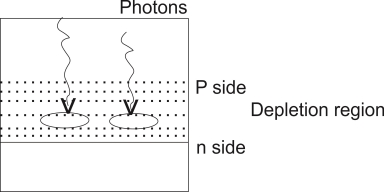
The light is always focused through a glass lens on the junction of the photodiode As the photodiode is reverse biased the depletion region is quite wide, penetrated on both side of the junction.
The photons incident on the depletion region will impact their energy to the Ions present in depletion region and generates e hole pairs.
The photons incident on the depletion region so the number of electron hole pairs will be generated depends on the intensity of light [number of photons] These and holes will be attracted towards the +ve& -ve terminals respectively of the photo current ,
With increase in the light intensity more number of e hole pairs are generated and the photo current increases thus the photocurrent is proportional to the light intensity.
Reference Books:
- “Digital Fundamentals” by Thomas. L. Floyd, 11th Edition, Pearson
2. “Mobile Communication” by J. Schiller, 2nd Edition, Pearson
3. “Sensors Handbook”, by S. Soloman, 2nd Edition.


