Unit – 2
Transistor and OPAMP
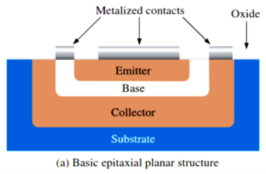
*BJT:-The BJT is constructed with the three draped semiconductors region’s separate by two Pn junctions as shown below
|
-Basic epitaxial planner structures.
-Three terminal with region’s are called emitter, base and collector.
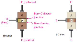
-The physical representation of the two types of BJT’s,
|
One type consists between two regions separated by a P region (npn) and other type consists of two p regions separated by an n region (pnp).
-The Pn junction joining the base region and the emitter region is called the base emitter junction.
-The Pn junction joining the base region and the collector region is called the base collector junction.
-The base region is lightly doped and very thin compared to the heavily doped emitter and the moderately doped collector regions.
*Base Transistor Operation:-
In order for the transistor to operate properly as an amplifier the two pn junction must be correctly biased with the external D.C vtg.
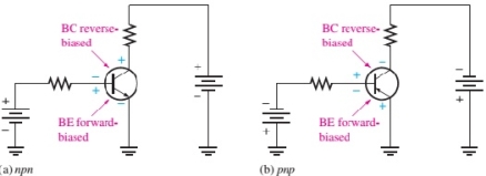
-The next figure shows the proper bias arrangement for both the npn and pnp transistors for active operation as an amplifier.
-In both the cases the base emitter
(BE) junction is forward biased & the base collector junction (BC) junction is reverse biased
|
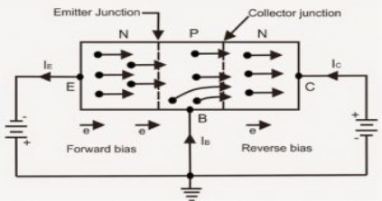
- As from above figure consider n-p-n transistor. The forward bias from base to emitter narrow’s the BE depletion region and the reverse bias from base to collector widens the BC depletion region shown in figure.
- The heavily doped N-TYPE emitter region is full with conduction band(frep) electron’s that easily diffuse through the forward biased BE junction into the p-type base region where they become minority carrier’s same as forward biased diode region
- The base region is lightly doped & very thin so that it has a very limited number of holes.
- Those only a small percentage of all the e-flowing the BE junction can combine with the available holes in the base.
- The relatively few recombined flow out of the base lead as valance electrons, forming as small base current.
- Most of the e flowing from the emitter into the thin lightly dooped base region do not recombine but diffuse into the BC depletion region.
- The BC depletion region diffuse e is being pulled across the reverse biased BC junction by the attraction of the collector supply vtg.
- The electrons now move through the collector region, out through the collector lead into the +ve terminal of the collector vtg source. This forms the collector electrons current.
- The collector current is much larger than the base current.
- This is the reason transistor exhibit current gain.
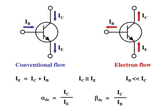
Transistor Current:-
|
Transistor’s Characteristic’s and parameters:-
-The transistors is connected to d.c bias vtg for both the npn&pnp types VBB forward biases the base emitter junction &Vcc reverse biases the base collector junction.
|
*Biasing conditions for different regions of operation:-
Sr. no | Region of operation | BE junction | CB junction | work |
1 | Cutoff region | R.B | R.B | S/w |
2 | Active region | F.B | R.B | Ampr |
3 | Saturation region | F.B | F.B |
|
Transistor’s Configuration:-
1) Common Base configuration(C.B)
2) Common emitter Configuration(C.E)
3) Common Collector Configuration(C.C)
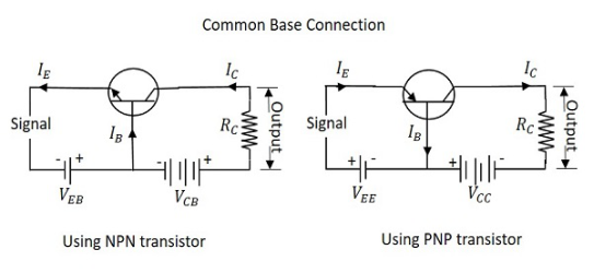
Common Base configuration(C.B):-
|
-The I/p is applied between the emitter and the base. The base acts as a common terminal between the I/p and o/p.
-The input vtg is therefore VEB and the input current is IE.
-The output is taken between the collector and the base therefore the output vtg is VCB and the output current is IC.
* Current relation’s in CB configuration:-
-The collector current is IC of the common base configuration is given by
Ic=Ic(INI)+ICBO
-Where the Ic(INI) called the injected collectors current and it is due to the number of electrons crossing the collectors base junction.
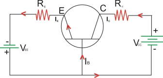
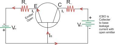
-ICBO :- This is the reverse saturation current flowing due to the minority carrier’s between the collector and base when the emitter is open
-ICBO flow’s due to the reverse biased collector’s base junction. As ICBO negligible as compared to Ic(INI) we can neglect it in practice.
.’. Ic=Ic(INI)………………………practically Ic=ICBO………………with emitter open
|
 Emitter is open
 ICBO
ICBO
Collector is to base control
-Since the ICBO flow’s due to terminally generated minority carrier’s it increases with increase the temperature.
-It doubles it’s value for every 100c rise in temperature.
-Current amplification factor or current gain (ddc):-
Current amplification factor or current gain is the ratio of collector current due to the injection to the total emitter current
αd.c = Ic(INI)
-The value of the ddc for CB configuration will always be less than 1.This is because
Ic(INI)<IE.
-Typically the value of d.d.c ranges between 0.95 to 0.995 depending upon the thickness of the base region.
-Larger the thickness of the base region smaller the value of the d.d.c
Ic(INI)=d.d.c.IE
Hence the expression for IC is given by
IC=αd.c IE + ICBo--------------------I
But the ICBo is negligibly small
IC d.d.c IE
* Expression for IB:-
IE=IB+IC
IE=αd.cIE+ICBo+IB…………………from I
IB=(1-αd.c)IE-ICBo
Neglecting ICBo
IB=(1-αd.c)IE
- Characteristics of a transistors in a common base configuration:-
1. Input Characteristic:-
A. Input Characteristic: is always a graph of input current verses input vtg. For common base (CB) configuration input current is the emitter current (IE) & I/p vtg. is the emitter to the base vtg (VEB)
The I/p Characteristic is plotted at a constant O/p vtg. VCB
|
B. Output Characteristic:
Output Characteristic is always a graph of O/p current versus O/p Vtg.
For the CB configuration the O/p current is collector current (IC) of the output voltage is collector to base vtg. (VCB)
Output Characteristic is plotted for a constant value of I/p current (IE)
|
O/p Characteristic of a n-p-n transistor in CB Configuration
Dynamic O/p resistance (ro)
ro =  / I
/ I  constant
in the active region Ic does not depend on VCB. It depends only on the I/p current IE. That is why the transistor is called as a current controlled or current operated device.
Feature of CB configuration :
- Common terminal : base
- Input current : IE
- O/p current IC
- I/P Vtg. : VEB
- O/P Vtg. VCB
- Current gain :
 ( less than 1)
 - Vtg. Gain : medium
- Input resistance : very low (20-)
- O/P resistance : very high (1 m-2)
- Application : as preamplifier
|
Common Emitter (CE) configuration
|
The important points about the CE
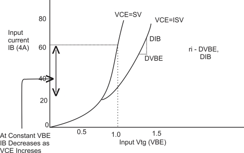
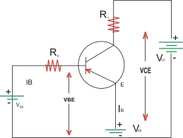
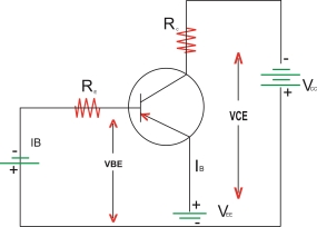
Configurations are as follows: the emitter acts as a common terminal between I/p and output. The /p Vtg. Is called between base and emitter
Hence VBE is the I/p Vtg. And IB is the input current.
The O/p is taken between the collector and emitter. There for VCE is the O/p Vtg. And IC is the O/p current.
In order to operate the transistor in its active region the base emitter (BE) junction is forward biased and collector base junction is reverse biased.
IE = IC + IB Where IC = Rearrange this eqn to get IC – ICBO =
IC
The value of
IC = But
1 +
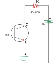
Put in eqn I IC = IC = Where ICEO is the reverse saturation current for the CE configuration which is given by ICEO = (1+
The Reverse leakage current of a transistor operating in the LE configuration is denoted by ICEO = (1 +
As the value of
put IB = 0
The Reverse leakage current (ICEO) Increases with increase in the temperature this current flows in the same direction as that of IC there for the collector current IC will increase with increase in temperature even when IB is constant
This is called as thermal instability so in CE configuration thermal stabilizing CKT must be included.
We know that IC Though ICEO is large it is much smaller as compared to
We know that
Similarly we can obtain the expression for
= Multiply & divide numerator & denominator for by IE
The value of dynamic input resistance ri is low for the CE configuration but it is not as low as that of CE configuration
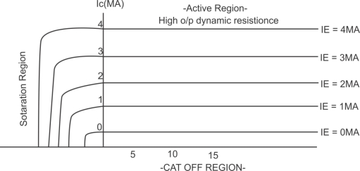
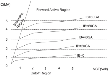
IB = 0 is cutoff region.
The collector current IC increases slightly with increase in the vtg.VCE. However the collector current is largely dependent on the base current IB At fixed value of VCE if IB is increased then it will cause IC to increase substantially. This is because IC = BIB this relation is true only for the active region of operation.
|
MOSFET : is another type of field effect transistor. The MOSFET has become one of the most important devices used in design and construction computers
MOSFET [metal oxide semiconductor field effect transistor]
Type of MOSFET
- Depletion type MOSFET
- Enhancement type MOSFET
- Power MOSFET
Enhancement type MOSFET : classified in to two type n. channel or p. channel E MOSFET
A) N-channel E MOSFET
B) P-channel E MOSFET
N-channel E MOSFET
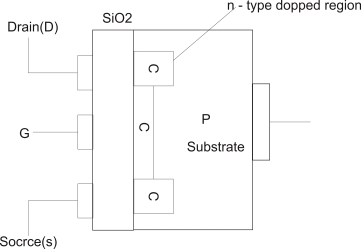
- A slab of P-type semiconductor is used as substrate. The substrate is sometimes connected to the source otherwise it is brought out as the fourth terminal.
- The drain and source terminal are connected to the n-type doped regions through the metallic contacts.
- The insulating sio2 layer is still present which isolates gate terminal from the substrate.
Effect of the insulting sio2 layer :
Due to the presence of the sio2 layer between gate terminal and n-type channel the i/p impedance of MOSFET is very high this is a desirable fracture of a MOSFET. Due to high i/p impedance the gate current IG= 0 for the d.c operating conditions.
Operation : the operation can be explained with two different operating
- Operation with VGS = 0
- Operation when VGS is +ve
1) Operating with VGS = 0 Volt
If VGS = 0 and a positive voltage is applied between its drain and source then due to the absence of the n-type channel a zero drain current will result.
2) Operation when Vgs Positive :
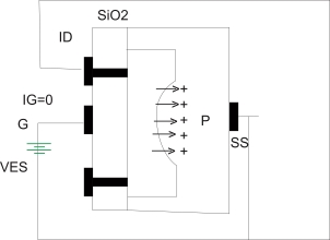
The positive potential at the gate terminal will repel the holes present in the p-type substrate.
|
Formation of induced channel in n-channel enhancement MOSFET
This creates a depletion region near the sio2 insulating layer. But the minority carriers ie the electrons in the p-type substrate will be attracted towards the gate terminal and gather near the surface of sio2 as shown above
As we increase the positive VGS the number of e- gathering near the sio2 layer increasesto such an extent that it creates an induced n-channel which connects the n-type doped regions.
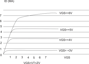
The drain current then starts flowing through this induced channel. The value of VGS at which this conduction begins is called as the threshold Vtg. & is indicated.
Characteristics of n-channel enhancement type MOSFET :
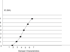
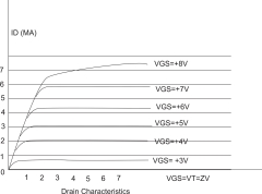
Transfer characteristics drain characteristics
P-channel enhancement type MOSFETS :
The construction of p-channel EMOSFET is exactly opposite to that of a n-channel EMOSFET
|
Characteristics:
Drain Characteristics of transfer Characteristics of p-channel E MOSFET
|
Operation : the operation can be explained with two different operating
Operation with VGS = 0
Operation when VGS is +ve
Operating with VGS = 0 Volt
If VGS = 0 and a positive voltage is applied between its drain and source then due to the absence of the n-type channel a zero drain current will result.
Operation when Vgs Positive :
The positive potential at the gate terminal will repel the holes present in the p-type substrate.
|
Formation of induced channel in n-channel enhancement MOSFET
- This creates a depletion region near the sio2 insulating layer. But the minority carriers ie the electrons in the p-type substrate will be attracted towards the gate terminal and gather near the surface of sio2 as shown above
- As we increase the positive VGS the number of e- gathering near the sio2 layer increasesto such an extent that it creates an induced n-channel which connects the n-type doped regions.
- The drain current then starts flowing through this induced channel. The value of VGS at which this conduction begins is called as the threshold Vtg. & is indicated.
Effect of increase in the drain to source Vtg. :
|
Effect of changes in VDS at fixed VGS on the channel width
- The positive gate to source voltage VDS is kept constant and the drain to source voltage VGS is increased gradually.
- Due to this the gate terminal becomes less and less positive with respect to the drain so less number of electron are attracted towards gate terminal & the induced channel becomes narrow.
- Eventually the channel width will be reduced to a point of pinch off and the saturation condition will be established which is same as that in a JFET
- That means any further increase in VDS at the fixed value of VGS will not affect the saturation level of ID unless breakdown condition are encountered.
- Symbols :
1) N-channel EMOSFET 2) P-channel EMOSFEJ
BJT is a bipolar device [minority & majority carriers both contributes to the current flow]
E MOSFET is a unipolar device ie current flows only due to the majority carriers
BJT thermal runaway can damage BJT thermal runway does not take place.
BJT low i/p impedance, E MOSFET High i/p impedance
- Voltage ampɤ :
- Current and vtg gain
|
In this expression if Ro is very small as compared to RL then Av A
A
Thus we can say that the overall gain of the ampɤie Av will approach its open circuit value A if Ro << RL
Prob : An amplifier has a signal i/p Vtg. Vi of 0.25v and draws 1mA from the source. The amɤ delivers & v to a load at 10 mA. Determine the current Vtg and power gains. Also find the i/p resistance of this ampɤ what must be the open ckt. Vtg of the source Vs to provide an ampɤ i/p VtgVi of 0.25 v when the internal resistance of the source is 50 Ω?
Given Vi = 0.25v, Ii = 1 Ma, Vo = 8 v, Io = 10 mA, Rs = 50 Ω.
Solution:
Vtg gain Av = 
Current gain =
= 
Power gain AP = Av  = 32
= 32 
Input resistance Ri =  = 250
= 250
Open circuit Vtg of Vs
Vi = 
Vs = 
Vs = 
Vs = 0.3v
MOSFET as switch :
- MOSFET can act as a switch jest like a transistor a typical switching Ckt using N-channel EMOSFET shown below
- A positive going i/p pulse (high i/p) turns on the EMOSFET. Maxm drain current flows and the o/p Vtg drops from +VDD to RD ID (on). So the EMOSFET acts as closed switch.
- Similarly when the i/p is low (zero) no drain current and hence the o/p is equal to +VDD. So the EMOSFET acts as open s/w
EMOSFET as an AMP :
The purpose of amplifier is to amplify the weak signal faithfully. For amplification MOSFET should operate in a saturation region.
|
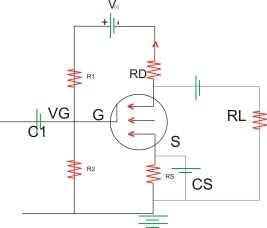
N-channel E-MOSFET Ampɤ
- It can operate with positive gate and drain Vtg where as in p-channel with –ve gate and drain Vtg
- For amplification MOSFET should operate in saturation region where the drain current
 remains constant
 - The threshold Vtg (VT) is the minimum gate Vtg (VGS) required to induce the channel between source to drain
- Fig shows single stage common source ampɤ using Vtg bias method
- Vin is A.c. signal
- Resistors R1 ,R2 and R5 provides the proper and stabilized operating point
- C in i/p coupling capacitor where is coat is the o/p coupling capacitor which blocks the d.c signal
- Cs is the bypass capacitor so that signal available at source terminal. never pass through Rs otherwise o/p Vtg reduces.
- It is commonly known as Op-amp.
- It requires an external power source hence is an active device.
- It is a versatile device that can be used to amplify ac as well as dc input signals.
- It can perform mathematical operations like addition, subtraction, multiplication, integration etc.
- Hence was named as Operational Amplifier due to its capability of performing mathematical operations.
- When external feedback is provided then the op-amp can be used as ac-dc signal amplifier, oscillator, regulator, active filter etc.
|
The block diagram of op-amp consists of :
- Types of inputs
- Non-inverting input
- Inverting input
- Input stage
- It has a dual input.
- It is a differential amplifier which provides balanced output.
- It provides voltage gain.
- Establishes input resistance of op-amp.
- Intermediate stage
- It also has a dual input.
- It is a differential amplifier which provides unbalanced output.
- The output of the input stage becomes input for the intermediate stage.
- Due to direct coupling, the dc voltage is well above 0V.
- Level shifting stage
- The output of the intermediate stage becomes input for the level shifting stage.
- It is an emitter follower with constant current source.
- It is used to shift dc level at the output to 0V wrto ground.
- Output stage
- This is the final stage.
- It’s a push pull amplifier.
- It raises swing in output voltage as well as increases current supply capability of op-amp.
An ideal op-amp is a differential input, single output device.
It has the following characteristics :
- Infinite input resistance [Ri =∞]
- Zero output resistance [RO = 0]
- Infinite voltage gain [AV = ∞]
- Infinite bandwidth [BW = ∞]
- Infinite Common Mode Rejection Ratio
- Infinite slew rate
- Zero offset [ ie,V1 = V2 , VO =0]
- The above characteristics do not change with the change in temperature .
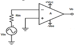
Inverting amplifier
V1 = 0V and V2 = Vin
Vout = A( - Vin ) where, A is the voltage gain of op-amp.
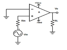
Non-Inverting Amplifier
V1 = Vin and V2 = 0V
Vout =AVin where, A is the voltage gain of op-amp.
|
Reference :
- “Digital Fundamentals” by Thomas. L. Floyd, 11th Edition, Pearson
2. “Mobile Communication” by J. Schiller, 2nd Edition, Pearson
3. “Sensors Handbook”, by S. Soloman, 2nd Edition.
