UNIT-6
Non Destructive Testing and Nano Technology
- Classification of Non-Destructive Testing Methods:
Non-destructive testing (NDT) is a combination of different inspection techniques used either individually or collectively to estimate the integrity and properties of the material, component or system without causing any damage.
Itrequires the use of one or more of those techniques once the inspection process is over.
NDT is mostly used for detection, characterization and sizing of inherent discontinuities, and those associated with damage mechanisms.
Many different NDT methods are used which include:
- Ultrasonic Testing
- Radiographic testing
- Electromagnetic testing
- Magnetic particle testing
- Liquid penetrant testing
- Visual Testing
- Principles of Physics in NDT
NDT is used
It is mainly used for testing physical methods which test materials, components and assemblies for flaws in the structure without any damage so that is can be used further.
It reveals the flaws in the structure of the product. However, it cannot predict how the flaws develop because of the design.
All NDT methods have the following characteristics:
- Application of testing medium for the product to be tested.
- Changes in testing medium because of the defects in the structure of the product.
- Means by which it detects these changes.
- Interpretation to these changes in order to obtain information about the flaws in the structure of the product.
- Advantages of Non-destructive Testing methods
- Defects can be easily detected without causing damage to the components.
- The methods can be applied easily,also quick and accurate.
- The equipment’s are easy to handle.
- The test results are recorded with ease on paper films, cassettes and floppies.
- Components are differentiated based on chemical, magnetic, electrical properties.
- Accuracy rate is highwhen measuring the components, thereby improving the product’s reliability.
- Acoustic Emission Testing (AET)
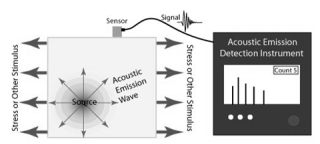
- The Acoustic Emission Testing technique is based on the detection and conversion of high frequency elastic waves to electrical signals. The waves generated are produced by the sudden redistribution of stress in the material.
- Whenever a structure is subjected to an external stimulus the localized sources triggers the release of energy, in the form of stress waves, which propagate to the surface and are recorded by sensors. This occurs when a small surface displacement of material is produced.
- When the component is stressed, the built-up state of stress spontaneously discharges at a leak, thereby generating sound impulses. The energy thus discharged is received by sensors applied on the surface of the tested object.
- The signals are received at different times by different sensors. By measuring these differences in time, the sound source can be located.
- One of the major advantages of AT is the possibility to test pressure equipment during plant operation or during downtimes caused by leaks, corrosions or defects of the material.
- The reliability of the information obtained through AE on the structural integrity of the tested object is greater than the conventional testing methods.
|
Figure 1. AET
2. Ultrasonic Testing (UT)
- Ultrasonic Testing (UT) is a technique that uses short, high-frequency ultrasonic sound waves to test the flaws in a material. They generally work by emitting ultrasonic waves into a material.
- By measuring these waves, the properties of the material and internal flaws can be detected. Most UT devices consist of many separate units.
- These separate unit includes receivers, transducers, and display monitors. The components included depend on the type of UT that the inspector is performing.
Basic Principle:
|
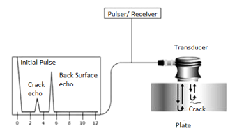
Figure 2. UT
- A typical pulse or echo ultrasonic testing inspection system consists of pulser or receiver.
- A high voltage electric pulses is produced by a pulser/reciever electronic device. The transducer generates high frequency ultrasonic energy, driven by a pulser.
- The sound energy is introduced and propagates through materials in the form of waves. When there is crack or discontinuity on the surface of component in the wave path ,part of the energy will be reflected back from the flaw surface .
- The reflected wave signal is transformed into a electrical signal by the transducer and is displayed on a screen.
- From the signal information about reflector location, size , orientation and other features can be gained.
Advantage of UT:
- It is sensitive to underneath and over surface discontinuities.
- The depth of penetration is comparatively superior to other NDT methods.
- Only single-sided access is needed when the pulse-echo technique is used.
- It has immense accuracy in determining reflector position and estimating size and shape.
- Minimal part preparation is required.
- Results are realtime.
- Electronic equipment provides instantaneous results.
- Detailed images can be produced with automated systems.
- In addition to flaw detection it also provides thickness measurement.
3. Radiography Testing (RT)
- Radiographic Testing (RT) is a non-destructive testing (NDT) method which uses either x-rays or gamma rays to examine the internal structure of the manufactured components by identifying any flaws or defects.
- It is suitable for testing welded joints that can be accessed from both sides, with the exception of double-wall signal image techniques used on some pipe.
- In industrial radiography there are several imaging methods available, techniques to display the final image that is Film Radiography, Real Time Radiography (RTR), Computed Tomography (CT), Digital Radiography (DR), and Computed Radiography (CR).
Basic Principle :
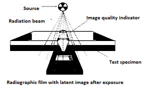
In RT, the part to be inspected is placed between a piece of radiation sensitive film and the radiation source. Radiation can be stopped by thicker and denser areas .
|
Figure 3. RT
Nanotechnology is the engineering of functional systems mostly at molecular scale. The manipulation and manufacture of materials and devices takes place on the scale of atoms or small groups of atoms.
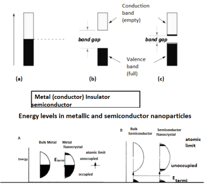
- Quantum confinement is the change of electronic and optical properties when the material sampled is of sufficiently small size - typically 10 nanometers or less.
- The bandgap increases when the size of the nanostructure decreases. Specifically, this phenomenon results from holes and electrons being squeezed into a dimension that approaches a critical quantum measurement, called the excitation Bohr radius.
- The first experimental evidence of the quantum confinement effects in clusters which occurs from crystalline CuCl clusters grown in silicate glasses .
- Spectroscopic studies on these clusters clearly indicated upto 0.1 eV blueshift of the absorption spectrum relative to the bulk. In the case of CdS clusters, the absorption threshold is observed to blueshift by 1eV or more as the cluster size is decreased . When the size of the cluster is smaller, the band gap is larger, and consequently the first absorption peak is shifted closer to the blue.
- Surface to volume ratio
It is defined as the amount of surface per unit volume of a nanoparticle. It is measured in inverse distance.
- Properties of nanoparticles:
Optical
Scattering, Absorption and Extinction
- When alight is incident on a nanoparticle, it can be scattered or absorbed. The sum of scattering and absorption is referred to as extinction.
- Nanoparticles are in the size regime where the fraction of light that is scattered or absorbed can vary greatly depending on the particle diameter.
- At diameters less than 20 nm, almost all of the extinction is due to absorption. At sizes above 100 nm, the extinction is mostly due to scattering.
- The optimal amount of scattering and absorption can be achieved by designing a particle with larger or smaller diameter.
- Another byproduct of the relationship between size and absorption/scattering is that aggregation can increase the effective size of a nanoparticle resulting in an increase in scattering.
- This is why 20 nm diameter silica particles are clear in solution but re-suspensions of dried 20 nm silica particles (aggregated) will be a milky white color.
Electrical :
|
Fig 4. Electronic band theory
Generlly properties like conductivity or resistivity are categorized as electrical properties. They are observed to change at nanoscale level similiar to optical properties.The change in electrical properties in nanomaterials include:
- Conductivity of bulk or large material does not depend upon dimensions like diameter or area of cross section and twist in the conducting wire.
- When force is given to nanotube the conductivity changes .
- The conductivity of single nanotube is different from multiwall carbon nanotube.
- The carbon nano tubes act as semiconductor or conductor in behaviour.
Mechanical:
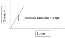
Elastic deformation refers to the change in the shape of the material at low stress which can be recovered after stress is removed.
|
Figure 5. Elastic deformation
According to Hooke’s law  = E
= E  where E = Young modulus(Pa) and
  is the stiffness of the material.
Hardness and strength
High hardness has been discovered among the nanostructured materials systems. A variety of superhard nanocomposites can be made of nitrides, borides and carbides by plasma-induced chemical and physical vapor deposition.
Ductility and Toughness:
In a conventional grain size regime, the reduction in grain size leads to an increase in ductility. Therefore, there is an increase in ductility as the grain size is reduced to nanoscale. On a very basic level, mechanical failure limits ductility, which is an interplay or competition between dislocations and cracks.
Applications of nanoparticles:
Medical
- Diagnostc techniques
Researchers at Worcester Polytechnic Institute are using antibodies attached to carbon nanotubes in chips to detect cancer cells in the blood stream. The researchers believe this method as it helps early detection of cancer cells in the bloodstream.
A test for early detection of kidney damage is also being developed. This method uses gold nanorods which is attached to the type of protein generated by damaged kidneys. When protein accumulates on the nanorod the color of the nanorod shifts. This test is designed for early detection which can be done quickly and inexpensively.
- Anti bacterial treatments
Researchers at the University of Houston are developing a technique to kill bacteria using gold nanoparticles and infrared light. This leads to improved cleaning of instruments in hospital settings.
Researchers at the University of Colorado Boulder are investigating the use of quantum dots to treat antibiotic resistant infections.
Electronic
- Nanoelectronics holds the promise of making computer processors more powerful than the conventional semiconductor fabrication techniques.
- A number of approaches are currently being researched, which include new forms of nanolithography and nanomaterials such as nanowires or small molecules in place of traditional CMOS components.
- Field effect transistors have been made using both semiconducting carbon nanotubeswith heterostructured semiconductor nanowires .
Space and Defence
o Propulsion systems
Most of rocket engines at present rely on chemical propulsion. All current spacecraft use some form of chemical rocket for launch and most use them for attitude control. Real rocket scientists though are actively researching new forms of space propulsion systems.
o Radiation shielding
- Radiation shielding is an area where nanotechnology makes major contribution to human space flight. NASA says that the risks of exposure to space radiation lies in factor of limiting humans’ ability to participate in long-duration space missions.
- Manyresearchers focus on developing countermeasures to protect astronauts from those risks. To meet the needs for radiation protection as well as other requirements such as low weight and structural stability. Spacecraft designers are looking for materials that help them develop multifunctional spacecraft hulls.
o Anti-satellite weapon countermeasure
- In order to meet emerging challenges posed by such ASAT missile systems, military strategists and researchers are developing novel technologies to protect their space assets.
- In view of this, Raytheon Company has developed a counter measure system using quantum dots to protect space assets such as satellites from missile attacks.
- They have developed a decoy consisting of quantum dots of different sizes and shapes that are engineered to emit radiation having a radiation profile similar to that of the asset.
Automobile
- Emission reduction
The catalytic converter helps to reduce the emissions from the automobiles through design and manufacturing by replacing the traditional metals such as cerium oxide and platinum. The catalytic converters utilize nano-sized rhodium and palladium in ceramics.
- Vehicle Computing
Spintronics is one of the new nanomagnetic materials to revolutionize vehicular computing systems. Many nanoparticles, such as silicon, organic semiconductors, CNTs, and graphene, are spin-injected into metals/oxides at an atomic level to replace the current microsystem.
Spintronics explains the aspects of electrons and their rotations, which could be influenced by both electric and magnetic fields. They are applied in recuperation technologies such as the reuse of braking energy.
- E-Mobility
Another successful application of nanotechnology is the bendable battery. This battery is simply made by coating a sheet of paper or plastic with an ink that has been incorporated with CNTs and Ag nanowires. This battery is flexible and easy to use in many automobile applications.
- Lubricants
A number of nanomaterials, such as nanostructured boric acid, tungsten nanospheres, copper nanoparticles, and graphene, have been used in car fluids. Adding nanoparticles to fluid lubricants can improve their mechanical properties and provide various economic benefits.
Reference:
1. Engineering Physics-Avadhanulu, Kshirsagar, S. Chand Publications
2. A textbook of optics- N Subrahmanyam and BriLal , S. Chand Publications
3. Engineering Physics- Gaur, Gupta, Dhanpat Rai and Sons Publications
