Unit 1
Introduction to Digital Electronics
- Operating Speed: High speed is required in the digital ICs. The speed of any gate is the time lapse between the input and the time in which the output is changed. The propagation delay should be the factor in consideration.
- Fan-In: It is the number of inputs that a gate can have like a two input AND gate has fan-in of two, a three input NAND gate as a fan-in of three etc. Hence a NOT gate has a fan-in of one. Normally delay increases as a quadratic function of fan-in.
- Fan-Out: The number of gates that each gate can drive, while providing voltage levels in the specified range is called the standard load or fan-out. It depends on the amount of electric current a gate can source or sink while driving other gates.
- Power Dissipation: Power dissipation of a circuit defines its battery life: the greater the power dissipation, the shorter the battery life. It is directly proportional to the heat generated by the chip or system hence excessive heat dissipation may increase operating temperature and cause gate circuitry to drift out of its normal operating range.
- Power Supply Requirements: There is normally one power supply to the chip denoted as Vcc. The main requirement for ICs is low power consumption.
- Noise Immunity:
Gate circuits are made to sustain variations in input and output voltage levels. Variations are usually the result of various factors. | |
| |
| |
| |
- Operating Temperature Range: Digital ICs should be capable of operating for temperature ranging from 00Cto 700C for consumers and from -550C to +1250C for military applications.
- Figure of Merit: Figure of merit is a product of propagation delay and power dissipation. It is measured in terms of Pico-Joules (ns ´mW = pJ). Current and voltage parameters define the minimum and maximum limit of current and voltage for input and output of a logic family.
They are built only with the help of transistors. It has been improved to meet performance requirements. TTL family comprises of: |
|
|
Operation of TTL NAND Gate (Two input)
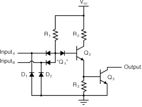
The circuit diagram of a 2 input TTL NAND gate is as follows:
- A two input TTL NAND is shown above. A and B are two inputs while Y is the output.
- Operation of the gate:
a) A and B both low: both B-E junctions of Q1 are forward biased. Hence D1 and D2 will conduct to force the voltage at point C to 0.7V. This voltage is insufficient to forward bias B-E junction of Q2. Hence Q2 remains OFF. Therefore its collector voltage rises to VCCVCC. As Q3 is operating in emitter follower mode, output Y will be pulled up to high voltage Y= 1
b) Either A or B low: If any one input is connected to ground with other left open or connected to VCCVCC the corresponding diode (D1 or D2) will conduct. This will pull down voltage at C o 0.7V. This voltage is insufficient to turn on Q2 so it remains OFF. So collector voltage of Q2 will be equal to VCC. This voltage acts as base voltage for Q3. As Q3 acts as an emitter follower, output Y will be pulled to VCCVCC. Y= 1
c) A and B both high: If both A and B are connected to then both diodes D1 and D2 will be reverse biased and do not conduct. Therefore D3 is forward biased and base current is supplied to transistor Q2 via R1 and D3. As Q2 conducts, the voltage at X will drop down and Q3 will be OFF, whereas voltage at Z will increase to turn ON Q4. As Q4 goes into saturation, the output voltage Y will be pulled down to low. Y = 0
TTL with active pull up
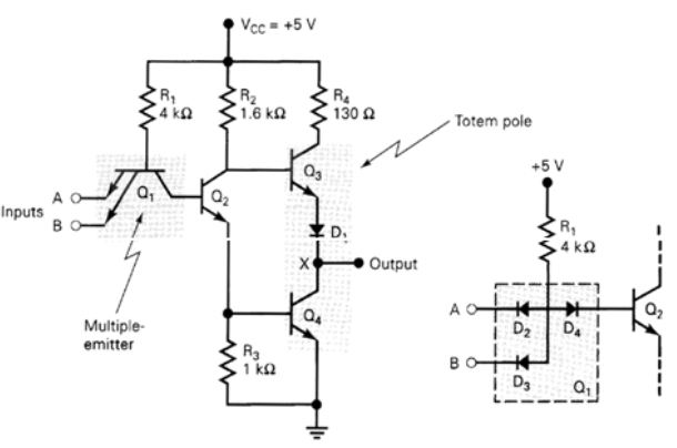
It is possible in TTL gates the charging of output capacitance without corresponding increase in power dissipation with the help of an output circuit arrangement referred to as an active pull-up or totem-pole output. In this case,
• Outputs must never be connected together.
• Connecting outputs causes excessively high currents to flow.
• Outputs will eventually be damaged.
• The standard TTL output configuration with a HIGH output and a LOW output transistor, only one of which is active at any time.
• A phase splitter transistor controls which transistor is active.
TTL with open collector output
The main feature is that its output is 0 when low and floating when high. Usually, an external Vcc may be applied.
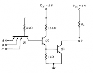
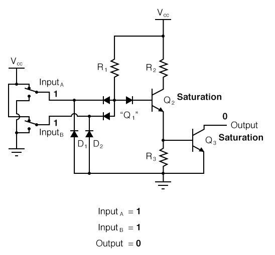
Transistor Q1 behaves as a cluster of diodes placed back to back. With any of the input at logic low, the corresponding emitter-base junction is forward biased and the voltage drop across the base of Q1 is around 0.9V, not enough for the transistors Q2 and Q3 to conduct. Thus the output is either floating or Vcc, i.e. High level.
Similarly, when all inputs are high, all base-emitter junctions of Q1 are reverse biased and transistor Q2 and Q3 get enough base current and are in saturation mode. The output is at logic low. (For a transistor to go to saturation, collector current should be greater than β times the base current).
Totem Pole Output:
Totem Pole means the addition of an active pull up the circuit in the output of the Gate which results in a reduction of propagation delay.
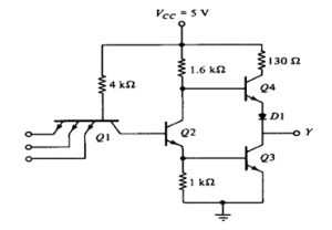
Logic operation is the same as the open collector output. The use of transistors Q4 and diode is to provide quick charging and discharging of parasitic capacitance across Q3. The resistor is used to keep the output current to a safe value.
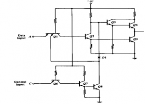
Three state Gate:
It provides 3 state output.
- Low-level state when a lower transistor is ON and an upper transistor is OFF.
- High-level state when the lower transistor is OFF and the upper transistor is ON.
- Third state when both transistors are OFF. It allows a direct wire connection of many outputs.
In the single-input (inverter) circuit, grounding the input resulted in an output that assumed the “high” (1) state. In the case of the open-collector output configuration, this “high” state was simply “floating.”
Allowing the input to float (or be connected to Vcc) resulted in the output becoming grounded, which is the “low” or 0 state. Thus, a 1 in resulted in a 0 out, and vice versa.
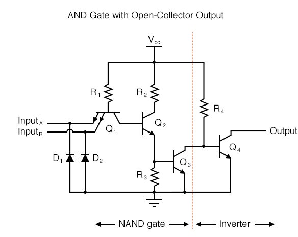
AND
To create an AND function using TTL circuitry, we need to increase the complexity of this circuit by adding an inverter stage to the output, just like we had to add an additional transistor stage to the TTL inverter circuit to turn it into a buffer:
Of course, both NAND and AND gate circuits may be designed with totem-pole output stages rather than open-collector. I am opting to show the open-collector versions for the sake of simplicity.
CMOS Inverter
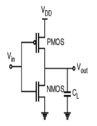
Fig: CMOS inverter
- It consists of PMOS and NMOS FET.
- The input A serves as the gate voltage for both transistors.
- The NMOS transistor has an input from Vss (ground) and PMOS transistor has an input from Vdd. The terminal Y is output.
- When a high voltage (~ Vdd) is given at input terminal (A) of the inverter, the PMOS becomes open circuit and NMOS switched OFF so the output will be pulled down to Vss.
- The truth table of inverter is:
A | Y = A’ |
0 | 1 |
1 | 0 |
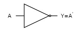
Fig. : NOT gate (ref. 1)
CMOS characteristics
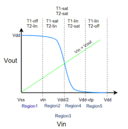
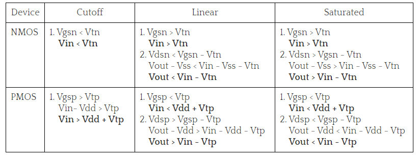
The VTC is divided into five regions(1-5) for easy of understanding. The above shown curve is possible when both T1 and T2 are matched for optimum operation. Optimum operation is achieved when Vin = Vdd/2 we get Vout = Vdd/2 . This can be achieved by adjusting width and length of both T1 and T2 as other parameters like mobility, oxide capacitance vary between different technologies.
Region-1
In this, the input is in the range of (0,Vtn).
- NMOS is in cutoff as Vgs < Vtn
- PMOS is in linear as Vgsp < Vtp and Vdsp > Vgsp -Vtp.
- Zero current flows from supply voltage and the power dissipation is zero.
Region-2
Here, the input is in the range of (Vtn,Vdd/2).
- NMOS is in saturation as Vgs > Vtn and Vout >Vin – Vtn.
- PMOS is in linear region as Vdsp > Vgsp -Vtp.
- Since both the transistors are conducting some amount of current flows from supply in this region.
Region-3
Here the input voltage is Vdd/2. At this point the output voltage is Vdd/2. Here both the NMOS and PMOS are in saturation and the output drops drastically from Vdd to Vdd/2. At this point a large amount of current flows from the supply.
- NMOS is in saturation as Vgs > Vtn and Vout >Vin - Vtn.
- PMOS is in saturation as Vgsp < Vtp and Vdsp < Vgsp -Vtp.
- Large amount of current is drawn from supply and hence large power dissipation.
Region-4
In this region the input voltage is in the range of (Vdd/2 , Vdd-Vtp). Here the PMOS remains in saturation as Vout < Vin - Vtp and Vgsp < Vtp. But the NMOS moves from saturation to linear region since the drain to source voltage now is less than Vgsn-Vtn.
- NMOS is in linear as Vgs > Vtn and Vout < Vin - Vtn.
- PMOS is in saturation as Vgsp < Vtp and Vdsp < Vgsp -Vtp.
- A medium amount of current is drawn as NMOS is in linear region and power dissipation is low.
Region-5
In this region the input voltage is in the range of (Vdd-Vtp,Vdd). Here the PMOS moves from saturation to cutoff as the Vgsp is so high that Vgsp > Vtp. The NMOS still remains in linear as the drain to source voltage now is less than Vgsn-Vtn.
- NMOS is in linear as Vgs > Vtn and Vout < Vin - Vtn.
- PMOS is in cutoff as Vgsp > Vtp.
- Zero current flows from the supply and hence the power dissipation is zero.
CMOS configurations- Wired Logic, Open-drain outputs
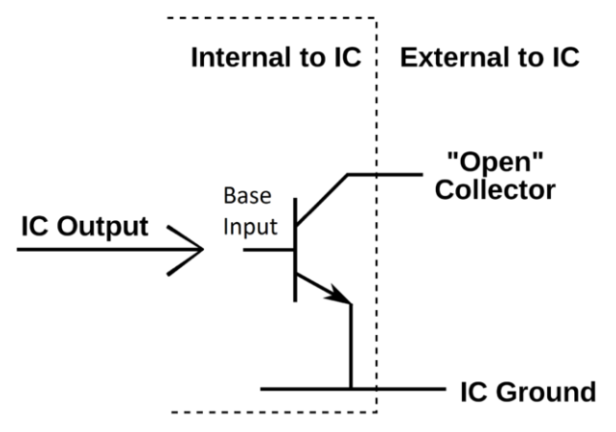
Open Drain is a type of programmable output port configuration with push pull,input only, and quasi-bidirectional configurations. Open-collector/open-drain is a circuit technique which allows multiple devices to communicate bidirectionally on a single wire. This is basically a mode which provides just a pull down operation.
An open collector/open drain is a common type of output found on many integrated circuits (IC). Instead of outputting a signal of a specific voltage or current, the output signal is applied to the base of an internal NPN transistor whose collector is externalized (open) on a pin of the IC. The emitter of the transistor is connected internally to the ground pin. If the output device is a MOSFET the output is called open drain and it functions in a similar way.
The CMOS NAND Gate is shown below. It has two transistors Q1 and Q3 connected in series and having the same input A. The transistor Q1 is turned ON when the input is high and the transistor Q3 is turned OFF during that period and viceversa.
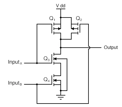
Fig: CMOS NAND Gate
The transistors Q2 and Q4 are connected in series having same input B. The transistors Q1 and Q2 have their source and drain connected in parallel. So, when any of the transistor amongst the two saturates the output goes HIGH. The transistors Q3 and Q4 have their source and drain connected in series. When both these transistors saturate the output goes LOW.
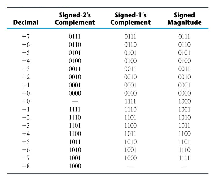
Signed Binary:

The table below shows all the signed four-bit binary numbers.
Binary Addition
- If both the signed magnitude numbers have same sign. We add both of them and the result is given common sign.
- If both the numbers have different signs, the smaller number is subtracted from the larger and the result is given the sign of larger number.
Binary Addition in 2’s compliment form:
- Both numbers are added with their sign bits and the carry bit is discarded.
Binary Subtraction in 2’s compliment form:
- We first find the 2’s compliment of the subtrahend and add with minuend. If carry is found at the signed bit then it is discarded.
For example: (-6)-(-13) = (11111010 – 11110011)
= (11111010+00001101)
= (00000111) = +7
1's complement
- Here, a number is obtained by changing all 1's to 0's and all 0's to 1's.
- This is called as 1's complement.
- For Example :
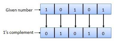
Fig.: 1's complement
2's complement
- It is obtained by adding 1 to the Least Significant Bit (LSB) of 1's complement of the number.
- Hence, 2's complement = 1's complement + 1
- For Example:
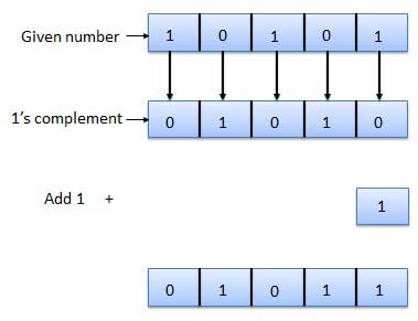
Fig.: 2's complement
It is an essential part of all the digital calculations.
Binary Addition
- It is a basis for binary subtraction, multiplication, division.
- There are four rules which are as follows:
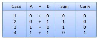
Fig.1 Rules of Binary addition
In fourth step, a sum (1 + 1 = 10) i.e. 0 is written in the given column and a carry of 1 over to the next column is done.
For Example −

Fig.2 Binary addition
Binary Subtraction
Subtraction and Borrow, these are the two words that will be used very frequently for binary subtraction. There rules of binary subtraction are:
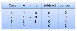
Fig.3 Rules of Binary Subtraction
For Example

Fig.4 Binary subtraction
Binary Multiplication
- It is similar to decimal multiplication.
- It is also simpler than decimal multiplication as only 0s and 1s are involved.
- There are four rules of binary multiplication which are:
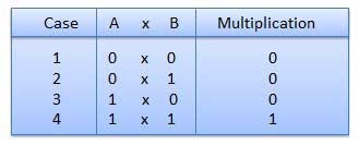
Fig.5 Rules of Binary Multiplication (Ref. 1)
For Example
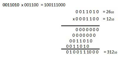
Fig.6 Binary Multiplication
Binary Division
- It is similar to decimal division.
- It is also called as the long division procedure.
For Example
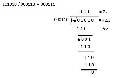
Fig.7 Binary Division
The process for subtraction of two binary numbers using 2’s compliment is:
- We take 2’s compliment of subtrahend.
- This is then added to the minuend.
- After the addition if carry obtained, it is discarded and the number is positive.
- If there is no carry after addition, we again take 2’s compliment of the result and the number is negative.
Q) Subtract the two binary numbers using 2’s compliment method 110110 – 10110?
Solution:
- Make number of bits equal for both numbers by padding 0 to the lesser.
- Now, 2’s complement of 010110 is (101101 + 1) i.e.101010. Adding this with the minuend.
1 1 0 1 1 0 Minuend
1 0 1 0 1 0 2’s complement of subtrahend
Carry over 1 1 0 0 0 0 0 Result of addition- As we have a carry so discarding it and the result is a positive number 100000.
This is the most common method for representation of real numbers on computers. To represent floating point numbers IEEE has set a standard. IEEE 754 numbers have basic components as listed below:
- The Sign of Mantissa –
This is as simple as the name. 0 represents a positive number while 1 represents a negative number. - The exponent –
The exponent field needs to represent both positive and negative exponents. A bias is added to the actual exponent in order to get the stored exponent. - The Normalised Mantissa –
The mantissa is part of a number in scientific notation or a floating-point number, consisting of its significant digits. Here we have only 2 digits, i.e. 0 and 1. So a normalised mantissa is one with only one 1 to the left of the decimal.
We can summarise the above as:
The exponent base is two. The exponent field contains 127 plus the true exponent for single-precision, or 1023 plus the true exponent for double precision. The first bit of the mantissa is typically assumed to be 1.
On the basis of above three components IEEE 754 can be categorised as
a) Single Precision: It is 8 bit exponent field.

The number ranges which the single precision floating point number cannot represent are:
i) Negative numbers less than −(2−2−23) × 2127
Ii) Negative numbers greater than −2−149
Iii) Zero
Iv) Positive numbers less than 2−149
v) Positive numbers greater than (2−2−23) × 2127
b) Double Precision

Few numbers which are still not defined in this standard are:
i) Denormalized: If the exponent is 0 the value is a denormalized number.
- Binary Coded Decimal (BCD) code
- Here each decimal digit is represented by a 4-bit binary number.
- It's a way to express each of the decimal digits with a binary code.
- Therefore, by four bits we can represent sixteen numbers (0000 to 1111).
- But in BCD code only the first ten of these numbers are used (0000 to 1001) and rest are invalid.

Fig.3: BCD codes (Ref. 1)
Advantages of BCD Codes
- It is very similar to the decimal system.
- We have to remember the binary equivalent of 0 to 9 only.
Disadvantages of BCD Codes
- The addition and subtraction of the BCD number system have different rules.
- The BCD arithmetic is more complicated.
- BCD code requires more number of bits than binary code to represent the decimal number.
- Hence is less efficient than binary.
2. Binary Code
- In coding, when alpha-numeric characters or words are represented by a specific group of symbols, it is said that it is being coded.
- The group of symbols is known as a code.
- The digital data can be represented, stored, and transmitted as a group of binary bits.
- This group is called a binary code.
- It is represented by the number as well as the alphanumeric character.
Advantages of Binary Code
- They are used in computer applications.
- They are suitable for digital communications.
- They make the analysis and designing of digital circuits easy.
- Implementation becomes very easy since only 0 & 1 are being used.
Classification of binary codes
The codes are broadly classified as:
- Weighted Codes
- Non-Weighted Codes
- Binary Coded Decimal Code
- Alphanumeric Codes
- Error Detecting Codes
- Error-Correcting Codes
Weighted Codes
- These codes obey the positional weight principle.
- Here each position represents a specific weight.
- Several systems are used to express the decimal digits 0 through 9.
- Here, each decimal digit is represented by a set of four bits.
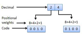
Fig.: Weighted codes (Ref. 1)
Non-Weighted Codes
- Here, the positional weights are not assigned.
- Example: Excess-3 code and Gray code.
3. Alphanumeric codes
A binary digit orbit can be represented by two symbols as '0' or '1'.
This is not sufficient for communication between two computers as we need many more symbols for communication.
These symbols represent 26 alphabetic characters with capital and small letters, numbers from 0 to 9, punctuation marks, and other symbols.
These alphanumeric codes represent numbers and alphabetic characters.
Most of them also represent other characters like symbols and various instructions necessary for conveying information.
The code at least represents 10 digits and 26 letters of alphabet i.e. total of 36 items.
The following three types of alphanumeric codes are commonly used for data representation.
- American Standard Code for Information Interchange (ASCII).
- Extended Binary Coded Decimal Interchange Code (EBCDIC).
- Five bit Baudot Code.
ASCII code is a 7-bit code whereas EBCDIC is an 8-bit code.
ASCII code is used worldwide while EBCDIC is primarily used in large IBM computers.
4. Error Codes
Their technique is available to detect and correct data during data transmission.
Error Code | Description |
Error Detection and Correction | Error detection and correction code techniques |
- It is also known as the XS-3 code.
- It is a non-weighted code used to express decimal numbers.
- They are derived from the 8421 BCD code words adding (0011)2 or (3)10 to each codeword in 8421.
- The excess-3 codes are obtained as −

Example
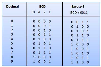
Fig.: BCD to XS 3 conversion (Ref. 1)
- It is the non-weighted code and is not an arithmetic code.
- This means that there are no specific weights assigned to the bit position.
- Here only one bit will change every time the decimal number is incremented.
- The gray code is also known as a unit distance code as only one-bit changes at a time.
- The gray code is a type of cyclic code.
- It cannot be used for all arithmetic operations.
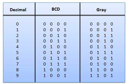
Fig.: Gray codes (Ref. 1)
Application of Gray code
- They are used in the shaft position encoders.
- This encoder produces a code word which represents the angular position of the shaft.
Representation of Logic Function
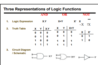
Logic Function of 2 Variables:
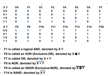
The Boolean expressions of any logic function ca be represented in the form of a table called as Truth Table. This table shows the input and output combinations depending on the circuit.
Truth Table for 2 variable is shown below.
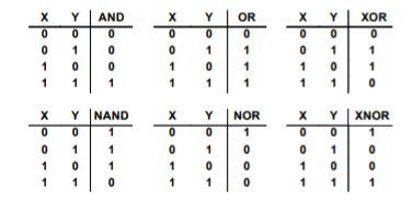
- Four product combinations is obtained by combining two variables x and y with logical AND operation. They are called as min terms or standard product terms. The min terms are given as x’y’, x’y, xy’ and xy.
- In the same way, four Boolean sum terms is obtained by combining two variables x and y with logical OR operation. They are called as Max terms or standard sum terms. The Max terms are given as x + y, x + y’, x’ + y and x’ + y’.
The following table represents the min terms and MAX terms for 2 variables.
x | y | Min terms | Max terms |
0 | 0 | m0=x’y’ | M0=x + y |
0 | 1 | m1=x’y | M1=x + y’ |
1 | 0 | m2=xy’ | M2=x’ + y |
1 | 1 | m3=xy | M3=x’ + y’ |
- If the binary variable is ‘0’, then it is represented as complement of variable in min term and as the variable itself in Max term.
- Similarly, if it is ‘1’, then it is represented as complement of variable in Max term and as the variable itself in min term.
- From the above table, we can easily notice that min terms and Max terms are complement of each other.
- If there are ‘n’ Boolean variables, then there will be 2n min terms and 2n Max terms.
Canonical SoP and PoS forms
- A truth table comprises of a set of inputs and output(s).
- If there are ‘n’ input variables, then there shall be 2n possible combinations comprising of zeros and ones.
- So the value of every output variable depends on the combination of input variables.
- Hence, each output variable have ‘1’ for some combination and ‘0’ for other combination of input variables.
Therefore, we can express each output variable in two ways.
- Canonical SoP form
- Canonical PoS form
Canonical SoP form
- It means Canonical Sum of Products form.
- In this, each product term contains all literals.
- So that these product terms are nothing but the min terms.
- Hence is also known as sum of min terms form.
- Firstly, identification of the min terms is done and then the logical OR of those min terms is taken in order to get the Boolean expression (function) corresponding to that output variable.
- This Boolean function will be in sum of min terms form.
- Then following the same procedure for other output variables too.
Example
Considering the following truth table.
Inputs | Output | ||
P | q | r | f |
0 | 0 | 0 | 0 |
0 | 0 | 1 | 0 |
0 | 1 | 0 | 0 |
0 | 1 | 1 | 1 |
1 | 0 | 0 | 0 |
1 | 0 | 1 | 1 |
1 | 1 | 0 | 1 |
1 | 1 | 1 | 1 |
- Here, the output (f) is ‘1’ for only four combinations of inputs.
- The corresponding min terms are given as p’qr, pq’r, pqr’, pqr.
- By doing logical OR, we get the Boolean function of output (f).
- Hence, the Boolean function of output is,
f = p’qr + pq’r + pqr’ + pqr.
- This is the desired canonical SoP form of output, f.
- It can also be represented as:
f=m3+m5+m6+m7f=m3+m5+m6+m7
f=∑m(3,5,6,7)f=∑m(3,5,6,7)
- First, we represented the function as sum of respective min terms and then, the symbol for summation of those min terms is used.
Canonical PoS form
- It means Canonical Product of Sums form.
- Here In this form, each sum term contains all literals.
- These sum terms are the Max terms.
- Hence, canonical PoS form is also known as product of Max terms form.
- Identification of the Max terms for which the output variable is zero is done and then the logical AND of those Max terms is done in order to get the Boolean expression corresponding to that output variable.
- This Boolean function is in the form of product of Max terms.
- Following the same procedure for other output variables too.
Standard SoP and PoS forms
Standard SoP form
- It stands for Standard Sum of Products form.
- In this, each product term need not contain all literals.
- So, the product terms can or cannot be the min terms.
- Therefore, it is therefore the simplified form of canonical SoP form.
Standard SoP of output variable can be obtained by two steps.
- Getting the canonical SoP form of output variable
- Simplification the above Boolean function.
The same procedure is followed for other output variables too, if there is more than one output variable.
Numerical
Convert the Boolean function into Standard SoP form.
f = p’qr + pq’r + pqr’ + pqr
Solution:
Step 1 – By using the Boolean postulate, x + x = x and also writing the last term pqr two more times we get
⇒ f = p’qr + pq’r + pqr’ + pqr + pqr + pqr
Step 2 – By Using Distributive law for 1st and 4th terms, 2nd and 5th terms, 3rdand 6th terms.
⇒ f = qr(p’ + p) + pr(q’ + q) + pq(r’ + r)
Step 3 – Then Using Boolean postulate, x + x’ = 1 we get
⇒ f = qr(1) + pr(1) + pq(1)
Step 4 – hence using Boolean postulate, x.1 = x we get
⇒ f = qr + pr + pq
⇒ f = pq + qr + pr
This is the required Boolean function.
Standard PoS form
- It stands for Standard Product of Sum form.
- Here, each sum term need not contain all literals.
- So, the sum terms can or cannot be the Max terms.
- Therefore, it is the desired simplified form of canonical PoS form.
Standard PoS form of output variable is obtained by two steps.
- Getting the canonical PoS form of output variable
- Simplification of the above Boolean function.
The same procedure is followed for other output variables too.
Numerical
Convert the Boolean function into Standard PoS form.
f = (p + q + r).(p + q + r’).(p + q’ + r).(p’ + q + r)
Solution:
Step 1 – By using the Boolean postulate, x.x = x and writing the first term p+q+r two more times we get
⇒ f = (p + q + r).(p + q + r).(p + q + r).(p + q + r’).(p +q’ + r).(p’ + q + r)
Step 2 – Now by using Distributive law, x + (y.z) = (x + y).(x + z) for 1st and 4thparenthesis, 2nd and 5th parenthesis, 3rd and 6th parenthesis.
⇒ f = (p + q + rr’).(p + r + qq’).(q + r + pp’)
Step 3 − Applying Boolean postulate, x.x’=0 for simplifying of the terms present in each parenthesis.
⇒ f = (p + q + 0).(p + r + 0).(q + r + 0)
Step 4 − Using Boolean postulate, x + 0 = x we get
⇒ f = (p + q).(p + r).(q + r)
⇒ f = (p + q).(q + r).(p + r)
This is the simplified Boolean function.
Hence, both Standard SoP and Standard PoS forms are Dual to one another.
- Karnaugh introduced a method for simplification of Boolean functions in an very easy way.
- This method is known as Karnaugh map method or K-map method.
- It is a graphical method, which comprises of 2n cells for ‘n’ variables.
- Here, the adjacent cells varies only in single bit position.
K-Maps for 2 to 5 Variables
It is the most suitable method for minimizing Boolean functions of 2 variables to 5 variables.
2 Variable K-Map
It has 4 number of cells since the number of variables is two.
The 2 variable K-Map is :

Fig.6 : 2 variable K-Map (ref. 1)
- The only way to group 4 adjacent min terms.
- The possible combinations are {(m0, m1), (m2, m3), (m0, m2) and (m1, m3)}.
3 Variable K-Map
It has 8 number of cells since the number of variables is 3.
The 3 variable K-Map is:
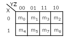
Fig.7 : 3 variable K-Map
- The only way to group 8 adjacent min terms.
- The possible are {(m0, m1, m3, m2), (m4, m5, m7, m6), (m0, m1, m4, m5), (m1, m3, m5, m7), (m3, m2, m7, m6) and (m2, m0, m6, m4)}.
- The possible combinations of grouping 2 adjacent min terms are {(m0, m1), (m1, m3), (m3, m2), (m2, m0), (m4, m5), (m5, m7), (m7, m6), (m6, m4), (m0, m4), (m1, m5), (m3, m7) and (m2, m6)}.
- If x=0, then 3 variable K-map becomes 2 variable K-map.
4 Variable K-Map
It has 16 number of cells since the number of variables is 4.
The 4 variable K-Map is:
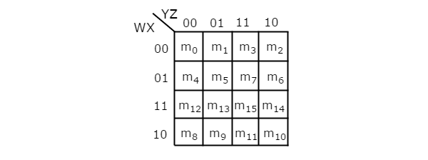
Fig.8 : 4 variable K-Map
- The only way to group 8 adjacent min terms.
- Let R1, R2, R3 and R4 represents the min terms of first row, second row, third row and fourth row respectively.
- Similarly, C1, C2, C3 and C4 represents the min terms of first column, second column, third column and fourth column respectively.
- The possible combinations are {(R1, R2), (R2, R3), (R3, R4), (R4, R1), (C1, C2), (C2, C3), (C3, C4), (C4, C1)}.
- If w=0, then 4 variable K-map becomes 3 variable K-map.
Rules for simplifying K-maps:
- Selecting K-map on the basis of number of variables present in the Boolean function.
- If the Boolean function is in Max terms form, then place the zeroes at respective Max term cells in theK-map.
- If the Boolean function is in PoS form, then place the zeroes wherever required in K-map for which the given sum terms are valid.
- The maximum possibilities of grouping is checked for adjacent zeroes.
- It should be of powers of two.
- Starting from highest power of two and to the least power of two.
- Highest power is equivalent to the number of variables considered in K-map and least power is zero.
- Each group will give either a literal or one sum term.
- It is known as prime implicant.
- The prime implicant is an essential prime implicant when at least a single ‘0’ is not covered with any other groups but only that grouping covers.
- The simplified Boolean function contains all essential prime implicants and only the required prime implicants.
Numericals
Simplify f(X,Y,Z)=∏M(0,1,2,4)f(X,Y,Z)=∏M(0,1,2,4)using K-map.

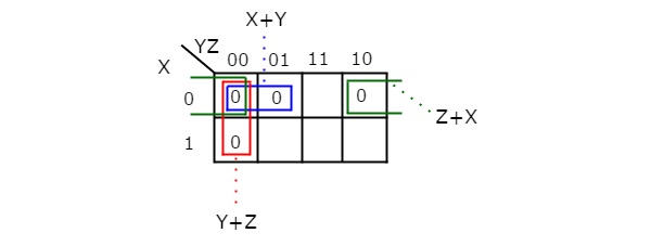
Therefore, the simplified Boolean function is
f = (X + Y).(Y + Z).(Z + X)
Simplify:
F(P,Q,R,S)=∑(0,2,5,7,8,10,13,15)
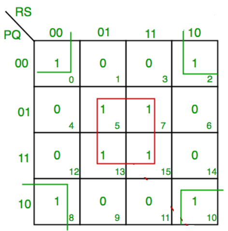
F = P’Q’R’S’ + PQ’R’S’ + P’Q’RS’ +PQ’RS’ + QS
F = P’Q’S’ + PQ’S’ + QS
F = Q’S’ +QS
Simplify:
F(A,B,C)=π(0,3,6,7)
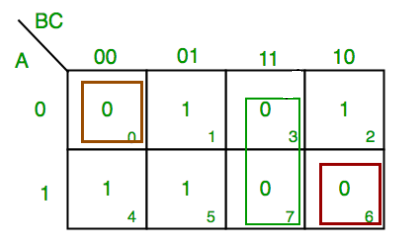
F = A’BC +ABC +A’B’C’ +ABC’
F = BC + C’ ( A’B’ + AB )