Unit 3
Sequential Logic Design
A Sequential circuit consists of inputs variable (X), logic gates and output variable (Z).
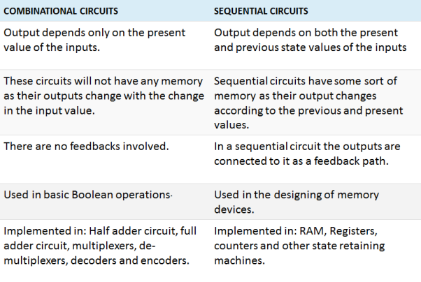
Combinational circuit generates an output on the basis of input variable only but Sequential circuit produces an output based on current input and previous output variables.
This means that it includes memory elements which are capable of storing binary information.
This binary information is nothing but the state of the sequential circuit at any given time. A latch capable of storing one bit information.

Fig. 1 Combinational circuit
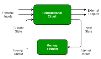
Fig. 2 Sequential circuit
There are two types of input to the combinational logic in fig 2 :
- External inputs which are not controlled by the circuit.
- Internal inputs which are function of previous output states.
Secondary inputs are state variables that are produced by the storage elements where as secondary outputs are excitations for those storage elements.
Types of Sequential Circuits –
There are two types of sequential circuit:
Asynchronous sequential circuit –
- They do not use a clock signal but instead uses the pulses as inputs.
- These circuits are faster because there is clock pulse and can change their state immediately when there is a change in the input signal.
- It is used when speed of operation is important and is independent of internal clock pulse.

Fig. 3 Asynchronous Sequential circuit
But they are more difficult to design and their output is also uncertain.
Synchronous sequential circuit –
- These circuit uses clock signal and level inputs.
- The output pulse is received in the same duration as the clock pulse for the clocked sequential circuits.
- They wait for the next clock pulse to arrive to perform the next operation, these circuits are bit slower as compared to asynchronous circuits.
- Level output changes state at the start of an input pulse and remains in that state until the next input or clock pulse arrives.
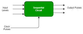
Fig. 4 Synchronous Sequential circuit
- It is used in synchronous counters, flip flops, and in MOORE-MEALY machines.
It is also used to design Counters
Latches are basic storage elements that operate with signal levels (rather than signal transitions). Latches controlled by a clock transition are flip-flops. Latches are edge-sensitive devices. Latches are useful for the design of the asynchronous sequential circuit.
SR (Set-Reset) Latch –
SR Latch is a circuit which has :
(i) 2 cross-coupled NOR gate or NAND gate.
(ii) 2 input S for SET and R for RESET.
(iii) 2 output Q and Q’.
Q | Q’ | STATE |
1 | 0 | Set |
0 | 1 | Reset |
Under normal conditions, both the input remains 0.
RS Latch with NAND gates:
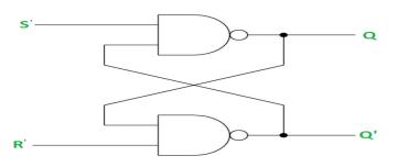
Case-1: When S’=R’=1 or S=R=0 then
If Q = 1, Q = R’ = 1.
If Q = 0, Q = 0 and R’ = 1 respectively.
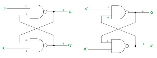
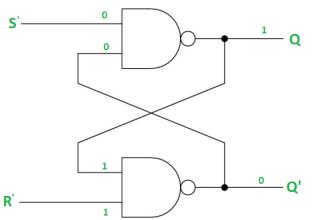
Case-2: S’=0, R’=1 (S=1, R=0)
As S’=0, Q = 1(SET state).
In 2nd NAND gate, as Q = R’ = 1, Q’=0.
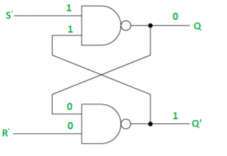
Case-3: S’= 1, R’= 0 (S=0, R=1)
As R’=0, Q’ = 1.
In 1st NAND gate, as Q =S’ = 1, Q=0 (RESET state).
Case-4: S’= R’= 0 (S=R=1)
When S=R=1, both Q = Q’ = 1 which is not allowed.
So, this input condition is prohibited.
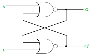
The SR Latch using NOR gate is:
Gated SR Latch –
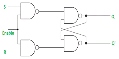
It is a latch which enable input that works when enable = 1 and retain the previous state when enable = 0.
Gated D Latch –
It is similar to SR latch with little modifications. Here, the inputs are complements of one another. The design of D latch with Enable signal is given below:
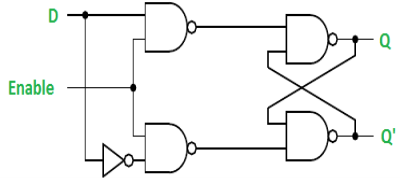
The truth table is shown below:
ENABLE | D | Q(N) | Q(N+1) | STATE |
1 | 0 | x | 0 | RESET |
1 | 1 | x | 1 | SET |
0 | x | x | Q(n) | No Change |
As the output is same as input, it is also known as Transparent Latch.
The characteristic equation for D latch with enable input is given as:
Q(n+1) = EN.D + EN'.Q(n)
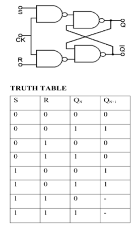
S-R Flip Flop :
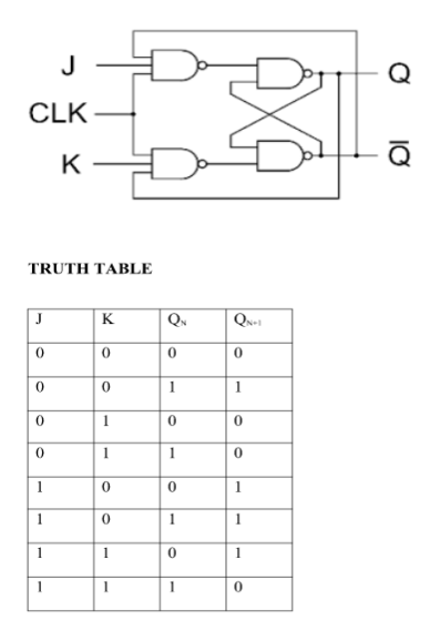
J-K Flip Flop:
D Flip Flop :

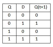
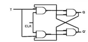
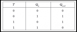
T Flip Flop :
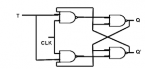

- RS Flip Flop
- JK Flip Flop
- D Flip Flop
- T Flip Flop
Logic diagrams and truth tables of the various types of flip-flops are as follows:
- S-R Flip Flop :

2. J-K Flip Flop:
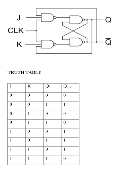
3. D Flip Flop :
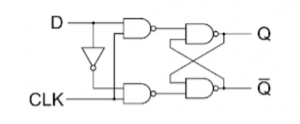

4. T Flip Flop :
- EXCITATION TABLE:
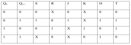
- i) SR To JK FlipFlop
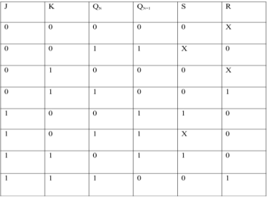
Excitation Functions:
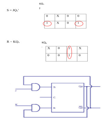
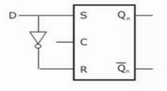
- Ii) Convert SR To D FlipFlop:
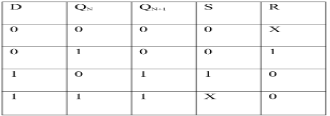
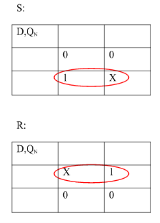
- Excitation Functions:
S = D
R = D‘
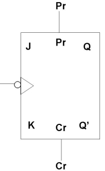
As flip flop may come up in random states when power is switched on, it is necessary to use some method where all the flip flops can be set or reset at the same time by a single switch – it is inconvenient to set or reset each flip flop individually. This is achieved by incorporating PRESET and CLEAR inputs in flip flops which can over-write all other inputs. These I/Ps are asynchronous and independent of the clock. While they are present, all other operations are inhibited. They force the output to a certain state irrespective of the I/Ps and clock.
Active High
Active High means that Preset and Clear I/Ps are inactive when low.
Pr = 1, Q = 1, Q’ = 0
i.e. if the Preset I/P is 1, the output will be forced to SET state irrespective of other I/Ps.
Cr = 1, Q = 0, Q’ = 1
i.e. if the Clear I/P is 1, the output will be forced to RESET state irrespective of other I/Ps.
It is not possible to Preset and Clear a flip flop at the same instant of time as Q can’t be 0 and 1 at the same time.
i.e. Pr = Cr ≠ 1 at any instant.
It is a combination of two JK flip-flops connected in series.
The first is the “master” and the other is a “slave”.
The output from the master is connected to the two inputs of the slave whose output is fed back to inputs of the master.
In addition to these two flip-flops, the circuit comprises an inverter.
The inverter is connected to clock pulse in such a way that an inverted clock pulse is given to the slave flip-flop.
In other words, if CP=0 for a master flip-flop, then CP=1 for a slave flip-flop and vice versa.
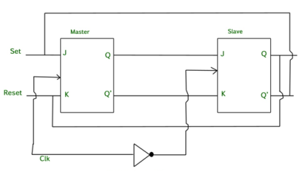
Fig. Master-Slave Flip flop
Working of a master-slave flip flop –
- When the clock pulse goes high, the slave is isolated; J and K inputs can affect the state of the system. The slave flip-flop is isolated when the CP goes low. When the CP goes back to 0, information is transmitted from the master flip-flop to the slave flip-flop, and output is obtained.
- The master flip flop is a positive level triggered and the slave flip flop is negative level triggered, hence the master responds before the slave.
- If J=0 and K=1, Q’ = 1 then the master goes to the K input of the slave and the clock forces the slave to reset therefore the slave copies the master.
- If J=1 and K=0, Q = 1 then the master goes to the J input of the slave and the Negative transition of the clock sets the slave and thus copy the master.
- If J=1 and K=1, the master toggles on the positive transition, and the slave toggles on the negative transition of the clock.
- If J=0 and K=0, the flip flop becomes disabled and Q remains unchanged.
Timing Diagram of a Master flip flop –
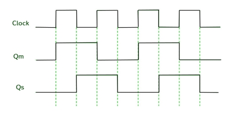
- When the CP = 1 then the output of master is high and remains high till CP = 0 because the state is stored.
- Now the output of the master becomes low when the clock CP = 1 and remains low until the clock becomes high again.
- Thus toggling takes place for a clock cycle.
- When the CP = 1 then the master is operational but not the slave.
- When the clock is low, the slave becomes operational and remains high until the clock again becomes low.
- Toggling takes place during the whole process since the output changes once in a cycle.
- This makes the Master-Slave J-K flip flop a Synchronous device that passes data with the clock signal.
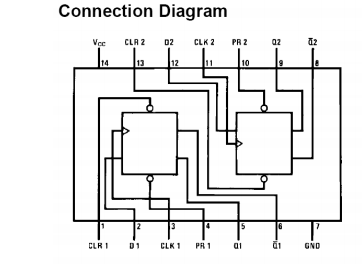
Pin 1, Clear 1 Input
Pin 2, D1 input
Pin 3, Clock 1 Input
Pin 4, Preset 1 Input
Pin 5, Q1 output
Pin 6, Complement Q1 output
Pin 7, Ground
Pin 8, Complement Q2 output
Pin 9, Q2 output
Pin 10, Preset 2 Input
Pin 11, Clock 2 Input
Pin 12, D2 input
Pin 13, Clear 2 Input
Pin 14, Positive Supply
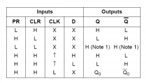
It is basically a dual D type edge triggered flip flop. The input is high on the positive edge of clock pulse. When the clock pulse is low or high the data in the D flip flop can be changed without changing the output. The input is reset when there is LOW logic level at the preset.
The value stored at particular value of clock cycle becomes the output. After that for different time the value of output does not change. It is widely used in data storage.
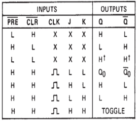
It is a dual JK flip flop. These flip flops are widely used as they can be reset with the clock input. This IC uses two JK flip flops. The pin diagram is shown below. It is a TTL based device.
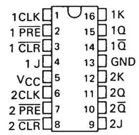
Pin1: CLK1
Pin2: PRE1
Pin3: CLR1
Pin4: Input1 (J)
Pin5: Vcc
Pin6: CLK2
Pin7: PRE2
Pin8: CLR2
Pin9: Input2 (J)
Pin10: 2Q’
Pin11: Output
Pin12: Input 2k
Pin13: GND
The Pin1 is input pin which provides clock pulse to the flip flop.The Pin2 makes the output of first flip flop HIGH. PIN3 is used to reset the output of first flip flop. Pin4 is the input pin of first flip flop. Pin5 is the supply or power pin. Pin6 is used to give clock pulse to second JK flip flop. Pin7 is the preset of second JK flip flop. Pin8 is clear input of second flip flop. Pin9 is the first input of second flip flop. Pin10 is second output of second flip flop. Pin11 is the first output of second flip flop. Pin12 is second input pin of second flip flop. Pin 13 is the ground pin.
- In this universal clock is not used and only the first flip flop is driven by main clock and the clock input of rest of the following is driven by output of previous flip flops.

Fig. Asynchronous counter
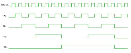
Fig. Timing diagram of Asynchronous counter
- It is seen from timing diagram that Q0 is changing as soon as the rising edge of clock pulse is encountered.
- Q1 is changing when rising edge of Q0 is encountered and so on.
- In this way ripples are generated through Q0,Q1,Q2,Q3 and therefore it is also called as a RIPPLE counter.
- It has one global clock which drives each and every flip flop and hence output changes in parallel.
- The advantage of synchronous counter over asynchronous counter is that it can operate on higher frequency and it does not have cumulative delay .
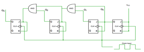
Fig. Synchronous counter
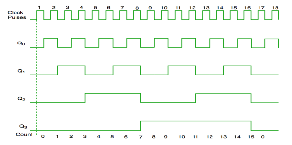
Fig. Timing diagram of synchronous counter
Modulo n counters
A modulo-N- counter is a counter that goes through a repeated sequence of N counts. For example, a 4-bit binary counter is a mod-16 counter.
Decade Counter
It counts ten different states and then reset to its initial states.
A simple decade counter will count from 0 to 9 but the decade counters which can go through any ten states between 0 to 15(for 4 bit counter) can also be made.
Truth table is as follows:
Clock pulse | Q3 | Q2 | Q1 | Q0 |
0 | 0 | 0 | 0 | 0 |
1 | 0 | 0 | 0 | 1 |
2 | 0 | 0 | 1 | 0 |
3 | 0 | 0 | 1 | 1 |
4 | 0 | 1 | 0 | 0 |
5 | 0 | 1 | 0 | 1 |
6 | 0 | 1 | 1 | 0 |
7 | 0 | 1 | 1 | 1 |
8 | 1 | 0 | 0 | 0 |
9 | 1 | 0 | 0 | 1 |
10 | 0 | 0 | 0 | 0 |
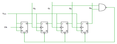
Fig. Decade counter
In the above circuit we used NAND gate for Q3 and Q1 and sending this to clear input line as the binary representation of 10 is—
1010
And Q3 and Q1 are 1 here, if we give NAND of these two bits then counter clears at 10 and again starts from the beginning.
This is basically a decade counter which counts upwards on applying the clock signal. It consists of four master-slave JK flip flops as divide by 2 and divide by 5 counters in it. It can store decimal digits in 4-bit binary numbers. The divide by 2 and divide by 5 counters can be used individually each by disabling the other or both simultaneously to produce MOD-10 counter.
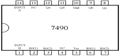
Fig: Pin Diagram of 7490
The pin configuration is explained below.
Pin1: clock input 2
Pin2: reset1
Pin3: reset2
Pin3: Not connected
Pin4: Supply voltage
Pin5: reset3
Pin6: reset4
Pin8: BCD output bit 2 (Qc)
Pin9: BCD output bit 1 (Qb)
Pin10: ground
Pin11: BCD output bit 3 (QD)
Pin12: BCD output bit 0 (QA)
Pin13: Not connected
Pin14: clock input 1
It is 4-bit binary decade counter with four outputs QA, QB, QC, QD. After the count value reaches 10 the binary output is reset. The MOD of this IC can be changed by the reset pins R0(1), R0(2), R9(1) and R9(2). If R0(1), R0(2) is high or R9(1) and R9(2) are ground the four outputs QA, QB, QC, QD are reset to 0000.
Applications:
a) As BCD Counter:
As we already know it consists of 4 master slave flip flops. The flip flop is triggered at negative edge of clock input.
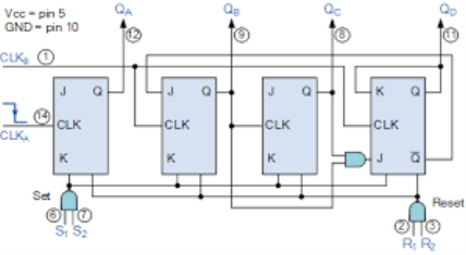
Fig: BCD Counter
When input is HIGH the reset R1 and R2 set the counter back to 0000. When S1 and S2 are HIGH the value of count is highest i.e 1001 no depending on the current counting status of the counter.
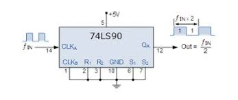
b) Divide by 2 counter:
It is used in frequency diving circuits. When the divide by 5 counter is disabled.
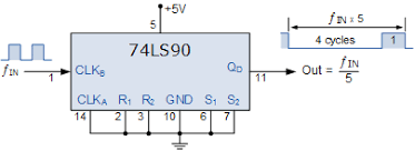
c) Divide by 5 counter:
The four input clock signals generate a 0 logic output and input clock signal produces 1 logic output.
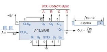
d) Divide by 10 counter:
Now both the counters are run simultaneously to generate divide by 10 counter. As QA first output from flip flop is not connected to next stage, we can extend it to form a 4-bit BCD counter by connecting QA to CLKB.
e) BCD decade counter:
The push button switch SW1 when released eery time will increase the count value by one. When the count due to SW1 reaches 1001 the outputs QA, QB, QC, QD are reset to 0000.
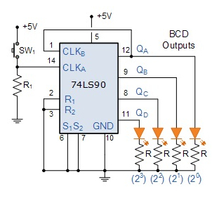
The truth table is already discussed in the above section.
- Flip flops are used to store one bit of binary data (1or 0).
- If we need to store multiple bits of data, we use multiple flip flops.
- N flip flops are connected to store n bits of data.
- A Register is a device that stores such information. It is a group of flip flops connected in series which is used to store multiple bits of data.
- The information stored in these registers can be transferred with the help of shift registers.
- This register is a group of flip flops used to store multiple bits of data.
- The bits stored in these registers can be moved in/out of the registers by applying clock pulses.
- The registers which shift the bits towards left are called “Shift left registers”.
The registers which shift the bits towards the right are called “Shift right registers”.
Shift registers are of 4 types and they are:
- Serial In Serial Out register
- Serial In the parallel Out register
- Parallel In Serial Out register
- Parallel In the parallel Out register
Serial-In Serial-Out Shift Register (SISO) –
- It allows serial input i.e. one bit after another and produces a serial output is known as Serial-In Serial-Out shift register.
- Since it has one output, the data leaves the register one bit at a time in a serial pattern, hence known as Serial-In Serial-Out Shift Register.
- The logic circuit is given underneath.
- The circuit comprises four D flip-flops which are connected serially.
- All these flip-flops are synchronous.

Fig. SISO
Serial-In Parallel-Out shift Register (SIPO) –
- It allows serial input through a single data line and produces a parallel output.
- The logic circuit is given underneath.
- The circuit consists of four D flip-flops which are connected synchronously.
- The clear (CLR) signal is also connected to all the 4 flip flops to RESET them.
- The output of the first flip flop is sent to the input of the next and so on.
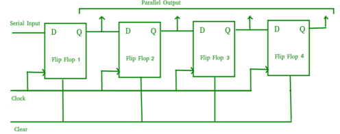
Fig. SIPO
- They are used in communication lines because the main use of the SIPO register is to convert serial data into parallel data.
Parallel-In Serial-Out Shift Register (PISO) –
- It allows parallel input data and produces a serial output.
- The logic circuit is given underneath.
- The circuit comprises four D flip-flops which are connected synchronously.
- The clock is connected to all the flip flops but the input data is connected to each flip flop individually through a multiplexer.
- The output of the previous flip flop and parallel data input are connected to the input of the MUX and the output of MUX is connected to the next flip flop.
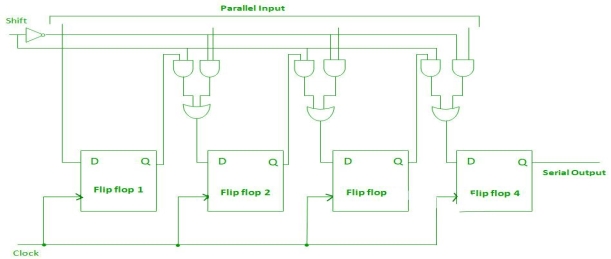
Fig. PISO
- It used to convert parallel data to serial data.
Parallel-In Parallel-Out Shift Register (PIPO) –
- It allows parallel input data and produces a parallel output.
- The logic circuit is given underneath.
- The circuit comprises four D flip-flops which are connected synchronously.
- The clear (CLR) and clock signals are connected to all flip flops.
- In this, there are no interconnections between flip-flops as no serial shifting of the data is required.
- Data is provided separately as input for each flip flop and the output is also collected individually from each flip flop.
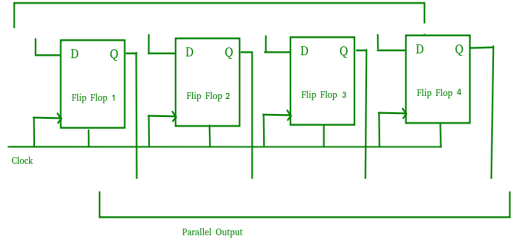
Fig. PIPO
- It is used as a temporary storage device and it acts as a delay element too.
Bidirectional Shift Register –
- If a binary number is shifted towards left by one position then it is equivalent to multiplying the number by 2 and if a binary number towards the right by one position then it is equal to dividing the number by 2.
- To perform the above operations a register is used which can shift the data in either direction.
- Hence, Bidirectional shift registers are capable of shifting the data either right or left depending on the mode selected.
- If the mode =1(high), then the data is shifted towards the right, and if the mode = 0(low), then the data is shifted towards the left direction.
- The logic circuit is given underneath.
- The circuit comprises four D flip-flops which are connected synchronously.
- The input data is connected at two ends of the circuit and depending on the model and gate selected.
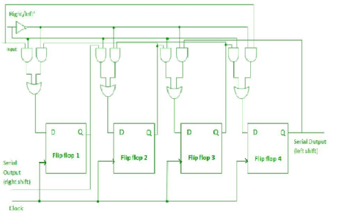
Fig. Bidirectional shift register