Unit 4
Computer Organization &Processor
- A computer organization describes the functions and design of the various units of a digital system.
- A general-purpose computer system is the best-known example of a digital system. Other examples include telephone switching exchanges, digital voltmeters, digital counters, electronic calculators and digital displays.
- Computer architecture deals with the specification of the instruction set and the hardware units that implement the instructions.
- Computer hardware consists of electronic circuits, displays, magnetic and optic storage media and also the communication facilities.
- Functional units are a part of a CPU that performs the operations and calculations called for by the computer program.
- Functional units of a computer system are parts of the CPU (Central Processing Unit) that performs the operations and calculations called for by the computer program. A computer consists of five main components namely, Input unit, Central Processing Unit, Memory unit Arithmetic & logical unit, Control unit and an Output unit.
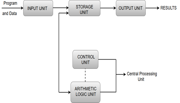
Input unit
- Input units are used by the computer to read the data. The most commonly used input devices are keyboards, mouse, joysticks, trackballs, microphones, etc.
- However, the most well-known input device is a keyboard. Whenever a key is pressed, the corresponding letter or digit is automatically translated into its corresponding binary code and transmitted over a cable to either the memory or the processor.
Central processing unit
- Central processing unit commonly known as CPU can be referred as an electronic circuitry within a computer that carries out the instructions given by a computer program by performing the basic arithmetic, logical, control and input/output (I/O) operations specified by the instructions.
Memory unit
- The Memory unit can be referred to as the storage area in which programs are kept which are running, and that contains data needed by the running programs.
- The Memory unit can be categorized in two ways namely, primary memory and secondary memory.
- It enables a processor to access running execution applications and services that are temporarily stored in a specific memory location.
- Primary storage is the fastest memory that operates at electronic speeds. Primary memory contains a large number of semiconductor storage cells, capable of storing a bit of information. The word length of a computer is between 16-64 bits.
- It is also known as the volatile form of memory, means when the computer is shut down, anything contained in RAM is lost.
- Cache memory is also a kind of memory which is used to fetch the data very soon. They are highly coupled with the processor.
- The most common examples of primary memory are RAM and ROM.
- Secondary memory is used when a large amount of data and programs have to be stored for a long-term basis.
- It is also known as the Non-volatile memory form of memory, means the data is stored permanently irrespective of shut down.
- The most common examples of secondary memory are magnetic disks, magnetic tapes, and optical disks.
Arithmetic & logical unit
- Most of all the arithmetic and logical operations of a computer are executed in the ALU (Arithmetic and Logical Unit) of the processor. It performs arithmetic operations like addition, subtraction, multiplication, division and also the logical operations like AND, OR, NOT operations.
Control unit
- The control unit is a component of a computer's central processing unit that coordinates the operation of the processor. It tells the computer's memory, arithmetic/logic unit and input and output devices how to respond to a program's instructions.
- The control unit is also known as the nerve center of a computer system.
- Let's us consider an example of addition of two operands by the instruction given as Add LOCA, RO. This instruction adds the memory location LOCA to the operand in the register RO and places the sum in the register RO. This instruction internally performs several steps.
Output Unit
- The primary function of the output unit is to send the processed results to the user. Output devices display information in a way that the user can understand.
- Output devices are pieces of equipment that are used to generate information or any other response processed by the computer. These devices display information that has been held or generated within a computer.
- The most common example of an output device is a monitor.
Processor Organization
To understand the organization of the CPU, let us consider the requirements placed on the CPU, the things that it must do:
- Fetch instruction: The CPU reads an instruction from memory.
- Interpret instruction: The instruction is decoded to determine what action is required.
- Fetch data: The execution of an instruction may require reading data from memory or an I/O module.
- Process data: The execution of an instruction may require performing some arithmetic or logical operation on data.
- Write data: The results of an execution may require writing data to memory or an I/O module.
To do these things, it should be clear that the CPU needs to store some data temporarily. It must remember the location of the last instruction so that it can know where to get the next instruction. It needs to store instructions and data temporarily while an instruction is being executed. In other words, the CPU needs a small internal memory.
Figure is a simplified view of a CPU, indicating its connection to the rest of the system via the system bus. You will recall (Lecture 1) that the major components of the CPU are arithmetic and logic unit (ALU) and a control unit (CU). The ALU does the actual computation or processing of data. The control unit controls the movement of data and instructions into and out of the CPU and controls the operation of the ALU. In addition, the figure shows a minimal internal memory, consisting of a set of storage locations, called registers.
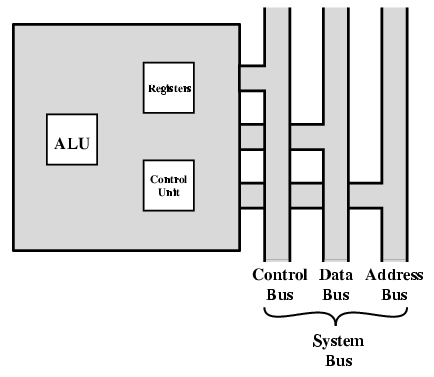
The CPU with the System Bus
Figure is a slightly more detailed view of the CPU. The data transfer and logic control paths are indicated, including an element labeled internal CPU-bus. This element is needed to transfer data between the various registers and the ALU because the ALU in fact operates only on data in the internal CPU memory.
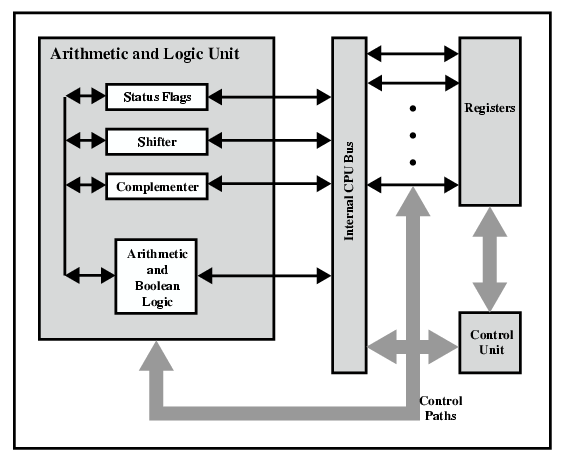
CPU Internal Structure
Register organization
Within the CPU, there is a set of registers that function as a level of memory above main memory and cache in the hierarchy. The registers in the CPU perform two roles:
- User-visible registers: These enable the machine- or assembly-language programmer to minimize main memory references by optimizing use of registers.
- Control and status registers: These are used by the control unit to control the operation of the CPU and by privileged, operating system programs to control the execution of programs.
There is not a clean separation of registers into these two categories. For example, on some machines the program counter is user visible (e.g., Pentium), but on many it is not (e.g., PowerPC). For purposes of the following discussion, however, we will use these categories.
User-Visible Registers
A user-visible register is one that may be referenced by means of the machine language that the CPU executes. We can characterize these in the following categories:
- General purpose
- Data
- Address
- Condition codes
General-purpose registers: can be assigned to a variety of functions by the programmer. Sometimes their use within the instruction set is orthogonal to the operation. That is, any general--purpose register can contain the operand for any opcode. This provides true general-purpose register use. Often, however, there are restrictions. For example, there may be dedicated registers for floating-point and stack operations. In some cases, general-purpose registers can be used for addressing functions (e.g.. Register indirect, displacement). In other cases, there is a partial or clean separation between data registers and address registers.
Data registers may be used only to hold data and cannot be employed in the calculation of an operand address.
Address registers may themselves be somewhat general purpose, or they may be devoted to a particular addressing mode. Examples include the following:
- Segment pointers: In a machine with segmented addressing, a segment register holds the address of the base of the segment. There may be multiple registers: for example, one for the operating system and one for the current process.
- Index registers: These are used for indexed addressing and may be autoindexed.
- Stack pointer: If there is user-visible stack addressing, then typically the stack is in memory and there is a dedicated register that points to the top of the slack. This allows implicit addressing; that is, push, pop, and other slack instructions need not contain an explicit stack operand.
Condition codes register (also referred to as flags): Condition codes are bits set by the CPU hardware as the result of operations. For example, an arithmetic operation may produce a positive, negative, zero, or overflow result. In addition to the result itself being stored in a register or memory, a condition code is also set. The code may subsequently be tested as part of a conditional branch operation.
Control and Status Registers
There are a variety of CPU registers that are employed to control the operation of the CPU. Most of these, on most machines, are not visible to the user. Some of them may be visible to machine instructions executed in a control or operating system mode.
Of course, different machines will have different register organizations and use different terminology. We list here a reasonably complete list of register types, with a brief description.
Four registers are essential to instruction execution:
- Program counter (PC): Contains the address of an instruction to be fetched.
- Instruction register (IR): Contains the instruction most recently fetched.
- Memory address registers (MAR): Contains the address of a location in memory.
- Memory buffer register (MBR): Contains a word of data lo be written to memory or the word most recently read.
Typically, the CPU updates the PC after each instruction fetch so that the PC always points to the next instruction to be executed. A branch or skip instruction will also modify the contents of the PC. The fetched instruction is loaded into an IR, where the opcode and operand specifiers are analysed. Data are exchanged with memory using the MAR and MBR. In a bus-organized system, the MAR connects directly to the address bus, and the MBR connects directly to the data bus. User-visible registers, in turn, exchange data with the MBR.
The four registers just mentioned are used for the movement of data between the CPU and memory. Within the CPU, data must be presented to the ALU for processing. The ALU may have direct access to the MBR and user-visible registers. Alternatively, there may be additional buffering registers at the boundary to the ALU: these registers serve as input and output registers for the ALL and exchange data with the MBR and user-visible registers.
All CPU designs include a register or set of registers, often known as the program status word (PSW), that contain status information. The PSW typically contains condition codes plus other stains information. Common fields or flags include the following:
- Sign: Contains the sign bit of the result of the last arithmetic operation.
- Zero: Set when the result is 0.
- Carry: Set if an operation resulted in a carry (addition) into or borrow (sub-traction) out of a high-order hit. Used for multiword arithmetic operations.
- Equal: Set if a logical compare result is equality.
- Overflow: Used to indicate arithmetic overflow
- Interrupt enable/disable: Used to enable or disable interrupts.
- Supervisor: Indicates whether the CPU is executing in supervisor or user mode. Certain privileged instructions can be executed only in supervisor mode, and certain areas of memory can be accessed only in supervisor mode.
A number of other registers related to status and control might be found in a particular CPU design. In addition to the PSW, there may be a pointer to a block of memory containing additional status information (e.g., process control blocks).
Example Register Organizations:
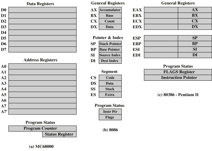
Example of microprocessor registers organizations
A memory is just like a human brain. It is used to store data and instructions. Computer memory is the storage space in the computer, where data is to be processed and instructions required for processing are stored. The memory is divided into large number of small parts called cells. Each location or cell has a unique address, which varies from zero to memory size minus one. For example, if the computer has 64k words, then this memory unit has 64 * 1024 = 65536 memory locations. The address of these locations varies from 0 to 65535.
Memory is primarily of three types −
- Cache Memory
- Primary Memory/Main Memory
- Secondary Memory
Cache Memory
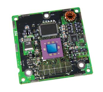
Cache memory is a very high speed semiconductor memory which can speed up the CPU. It acts as a buffer between the CPU and the main memory. It is used to hold those parts of data and program which are most frequently used by the CPU. The parts of data and programs are transferred from the disk to cache memory by the operating system, from where the CPU can access them.
Advantages
The advantages of cache memory are as follows −
- Cache memory is faster than main memory.
- It consumes less access time as compared to main memory.
- It stores the program that can be executed within a short period of time.
- It stores data for temporary use.
Disadvantages
The disadvantages of cache memory are as follows −
- Cache memory has limited capacity.
- It is very expensive.
Primary Memory (Main Memory)
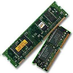
Primary memory holds only those data and instructions on which the computer is currently working. It has a limited capacity and data is lost when power is switched off. It is generally made up of semiconductor device. These memories are not as fast as registers. The data and instruction required to be processed resides in the main memory. It is divided into two subcategories RAM and ROM.
Characteristics of Main Memory
- These are semiconductor memories.
- It is known as the main memory.
- Usually volatile memory.
- Data is lost in case power is switched off.
- It is the working memory of the computer.
- Faster than secondary memories.
- A computer cannot run without the primary memory.
Secondary Memory
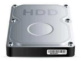
This type of memory is also known as external memory or non-volatile. It is slower than the main memory. These are used for storing data/information permanently. CPU directly does not access these memories, instead they are accessed via input-output routines. The contents of secondary memories are first transferred to the main memory, and then the CPU can access it. For example, disk, CD-ROM, DVD, etc.
Characteristics of Secondary Memory
- These are magnetic and optical memories.
- It is known as the backup memory.
- It is a non-volatile memory.
- Data is permanently stored even if power is switched off.
- It is used for storage of data in a computer.
- Computer may run without the secondary memory.
- Slower than primary memories.
I/O is one of those concepts that can seem self-explanatory. But simple as they may seem, inputs and outputs are a building block of modern electronics.
Inputs and outputs are fundamental to the world of computing (and more generally in data/information processing). Without them, electronic devices of all kinds would have no way of receiving data, and the user would have no way of manipulating or interacting with that data. Since they form the basis of our relationship with almost all the devices we use, it’s important to understand how inputs and outputs function.
What is Input and Output?
Simply put, inputs and outputs are the ways that a computer (or another device) interacts with the world.
Inputs refer to any way that the computer receives data from outside world. The most obvious examples are your computer’s keyboard, trackpad, or mouse, but “inputs” can also include cameras, microphones, and other devices or systems that supply data to a given computer.
Outputs operate similarly, but in reverse. Outputs enable computers to address the physical world; these devices include displays and speakers, but also controls and signals for tasks like turning lights off and on, controlling motors, and more.
How Computer Input and Output Works
Generally, I/O devices communicate with a computer through an interface called a bus. This interface has two main functions.
1. Interpreting. The bus addresses and performs “handshaking” between the devices using basic commands (like “READY” or “BUSY”). This handshaking allows the devices to communicate with each other successfully.
2. Converting. The interface’s second function is to convert data from serial to parallel or vice versa when necessary. This conversion is what allows devices with different types of information to communicate.
Computers and most other digital systems operate in binary, so any input signal must be in binary by the time it arrives at the computer’s processor. Therefore, any analog inputs go through a conversion to digital using an 9*6+69999999999999999999999) – though that is often part of the device/peripheral itself, as in the case of a scanner. The digital signal that results may also need conversion, as mentioned above, since digital data can be either serial or parallel. At this stage, the bus can typically facilitate conversion between types of digital data.
Conversely, an output bus will facilitate the conversion of the computer’s data into whatever form is needed, whether it’s audio, video, or something else. In some cases, such as with audio, digital information will convert back into analog. Users will need to employ a digital-to-analog converter (DAC) to allow the data to be used with real-world devices.
What is GPIO?
A general-purpose input/output (GPIO) is a digital data pin on a circuit (either an integrated circuit or electronic circuit board). A user may change the GPIO’s function at run time and manipulate the pins to operate as inputs or outputs.
Most GPIOs cannot output enough current to power devices like lightbulbs or motors on their own. To use a GPIO to control such a device, you’ll typically need to use a transistor and/or relay to directly power it.
I/O Functions
The SAS/C library provides a large set of input/output functions. These functions are divided into two groups, standard I/O functions and UNIX style I/O functions.
The library's I/O implementation is designed to
- Support the ISO/ANSI C standard
- Support the execution of existing programs developed with other C implementations
- Support the development of new portable programs
- Support the effective use of native OS/390 and CMS I/O facilities and file types.
The library provides several I/O techniques to meet the needs of different applications. To achieve the best results, you must make an informed choice about the techniques to use. Criteria that should influence your choice are
- The need for portability (For example, will the program execute on several different systems?)
- The required capabilities (For example, will the program need to alter the file position randomly during processing?)
- The need for efficiency (For example, can the program accept some restrictions on file format to achieve good performance?)
- The intended use of the files (For example, will files produced by the program later be processed by an editor or by a program written in another language?).
To make these choices, you need to understand general C I/O concepts as well as the native I/O types and file structures supported by the 370 operating systems, OS/390 and CMS.
Details about C I/O concepts and functions can be found in I/O Functions.
The I/O functions are
Afflush | Flush file buffers to disk |
Afopen | Open a file with system-dependent options |
Afread | Read a record |
Afread0 | Read a record (possibly length zero) |
Afreadh | Read part of a record |
Afreopen | Reopen a file with system-dependent options |
Afwrite | Write a record |
Afwrite0 | Write a record (possibly length 0) |
Afwriteh | Write part of a record |
Aopen | Open a file for UNIX style access with amparms |
Clearerr | Clear error flag |
Close | Close a file opened by open |
_close | Close an HFS file |
Closedir | Close a directory |
Clrerr | Clear error flag and return status |
Creat | Create and open a file for UNIX style I/O |
Ctermid | Get a filename for the terminal |
Dup | Duplicate a file descriptor |
Dup2 | Duplicate a file descriptor to a specific file descriptor number |
Fattr | Return file attribute information |
Fclose | Close a file |
Fcntl | Control open files or sockets |
_fcntl | Control open file descriptors for UNIX System Services (USS) HFS files |
Fdopen | Access an USS file descriptor via standard I/O |
Feof | Test for end of file |
Ferror | Test error flag |
Ffixed | Test for fixed-length records |
Fflush | Flush output buffer |
Fgetc | Read a character from a file |
Fgetpos | Store the current file position |
Fgets | Read a string from a file |
Fileno | Return file descriptor number |
Fnm | Return filename |
Fopen | Open a file |
Fprintf | Write formatted output to a file |
Fputc | Write a character to a file |
Fputs | Write a string to a file |
Fread | Read items from a file |
Freopen | Reopen a file |
Fscanf | Read formatted input from a file |
Fseek | Reposition a file |
Fsetpos | Reposition a file |
Fsync | Flush buffers for a UNIX style file to disk |
_fsync | Flush HFS file buffers to disk |
Ftell | Obtain the current file position |
Fterm | Terminal file test |
Ftruncate | Truncate an USS file |
Fwrite | Write items to a file |
Getc | Read a character from a file |
Getchar | Read a character from the standard input stream |
Gets | Read a string from the standard input stream |
Isatty | Test for terminal file |
Kdelete | Delete current record from keyed file |
Kgetpos | Return position information for keyed file |
Kinsert | Insert record into keyed file |
Kreplace | Replace record in keyed file |
Kretrv | Retrieve next record from keyed file |
Ksearch | Search keyed file for matching record |
Kseek | Reposition a keyed stream |
Ktell | Return RBA of current record |
Lseek | Position a file opened for UNIX style access |
_lseek | Position an USS HFS file |
Open | Open a file for UNIX style I/O |
_open | Open an USS HFS file |
Opendir | Open an USS HFS directory |
Pclose | Close a pipe opened by popen |
Pipe | Create and open a pipe |
Popen | Open pipe I/O to an USS shell command |
Printf | Write formatted output to the standard output stream |
Putc | Write a character to a file |
Putchar | Write a character to the standard output stream |
Puts | Write a string to the standard output stream |
Read | Read data from a file opened for UNIX style access |
_read | Read data from an USS HFS file |
Readdir | Read an USS directory entry |
Rewind | Position to start of file |
Rewinddir | Positions an USS directory stream to the beginning |
Scanf | Read formatted data from the standard input stream |
Setbuf | Change stream buffering |
Setvbuf | Change stream buffering |
Snprintf | Write a limited amount of formatted output to a string |
Sprintf | Write formatted output to a string |
Sscanf | Read formatted data from a string |
Tmpfile | Create and open a temporary file |
Tmpnam | Generate temporary filename |
Ttyname | Get name of open terminal file |
Ungetc | Push back an input character |
Vfprintf | Write formatted output to a file |
Vprintf | Write formatted output to the standard output stream |
Vsnprintf | Write a limited amount of formatted output to a string |
Vsprintf | Write formatted output to a string |
Write | Write data to a file open for UNIX-style access |
_write | Write data to an USS HFS file. |
Types of I/O
There are three types of I/O operations:
Sensory input
- Digital input
- Analog input
Control output
- Direct digital output
- Modulated digital output
- Analog output
Data transfer
- Parallel
- Serial
Notes:
I/O is one of the three main components of a computer system. The responsibility of I/O is to interface with external devices. Depending on their applications, I/O operations can be divided into three groups: sensory input, control output, and data transfer. Once the nature of each type of I/O operation is understood, the hardware design and software for these operations can be understood easily.
Like memory components, I/O components have addresses and each I/O address usually consists of 8 or 16 bits of data. Since many sensory input and control output signals consist of just one bit of information, a single I/O address may be able to handle multiple input and output signals. For instance, some bits of an 8-bit port can be used to receive input signals while other bits are used to send output signals. Depending on how they are used, one bit of an I/O address may be referred to as an I/O port or the set of all bits at a single I/O address may be referred to as an I/O port. When someone says how many ports are needed, you need to find out what his or her definition of port is.
The System Bus
An external bus is a communication path between the major components of a computer system such as the CPU and the PM. A bus within the CPU is called an internal bus. Many systems have multiple external buses. Here we limit our discussion to a single external bus, which we call the system bus (or just the bus), that connects the CPU to all the other components of a simple computer system.

The bus is not directly connected to the CPU, the PM, the secondary storage units, and the IO devices. Instead it is connected to each of these unit's controller. The DMA is not a device, but a special kind of control unit that participates in transfers to and from secondary storage units such as the disk and the CD. A bus transaction consists of a two-way communication between two components, during which the bus is normally unavailable for any other communication. The component that initiates a bus transaction is called the initiator, the bus master, or just the master. The master issues a request, such as a read or write, to some other component, which is called the responder or the slave. Common master-slave pairs are BIU-PMC, BIU-IOC, and DMA-PMC. A transaction begins when the master issues a request and ends when the requested action has finished. A particular bus always uses same set of rules for communication between the master and the slave. This set of rules is called the bus protocol and every device attached to the bus must follow these rules. SCSI (small computer system interface), PCI (peripheral component interconnect), and EISA (extended ISA; ISA was the original IBM AT bus) are common protocols found in PCs.
The bus consists of three types of wires, called lines. The control lines, which are collectively called the control bus, transmit the kind of bus transaction (e.g., READ, WRITE) and other information from the master to the slave. In addition the control bus transmits return signals from the slave to the master (e.g., MRC). The address lines, collectively called the address bus, transmit the address of the location within the slave of the data that is to be read (read transaction) or the location into which the data is to be written (write transaction). The data lines, which are collectively called the data bus, transmit the data that is being read or written. Note that even though each of these three sets of lines is called a bus, all of these lines are actually part of the same single bus (the system bus).
A bus has a clock and one period of that clock constitutes a bus cycle, or a bus clock (BCLK) as opposed to a processor (CPU) clock (PCLK). A BCLK is much longer than PCLK. High performance PCs may have a 100 MHz, or slightly higher, bus coupled with a 700 MHz to 1 GHz processor. Normally, the minimum time to transfer a request from the master to a slave or to transfer a response from the slave to the master is one BCLK.
Bus Arbitration
During one BCLK, one and only one of the components connected the bus is the bus master, each of the other devices is either a slave or inactive. The bus master initiates a bus transfer, while the slave is passive because it can only wait for a request from the bus master. This relationship is not always fixed, for example, either the BIU or the DMA can be a master with the PMC as a slave. The bus arbiter resolves simultaneous requests for use of bus. The two major types of arbiters are centralized and distributed.
A centralized arbiter is a single component that always makes the decision. As shown in the figure below, all the devices are connected in parallel to both the bus request line (BR') and the bus busy line (BBSY'), and in series to the bus grant line (BG). If a device wants the bus, it asserts BR' and then waits. When it sees its BGi asserted, it checks BBSY'. If BBSY' is asserted, it waits until it is deasserted and then it starts its bus transaction. The serial connection of all the devices to the bus grant line is called a daisy chain. Each device in the chain passes the BG signal on to the next device in the chain unless it has requested the bus, in which case it does not pass the signal. In a daisy chain, if more than one device has requested the bus at the same time, the one that is closest to the arbiter on the chain has the highest priority and will get the bus.

In a distributed arbiter all devices are connected to a common set of request lines. Each device knows its own priority. When a device wants the bus, it outputs its priority onto the request lines and then reads the request lines. If the request lines contain that device's priority code then it is the highest priority requester, so it gets the bus. All other devices will see a code higher than their priority and will defer use of bus.
Synchronous and Asynchronous Buses
Buses come in two flavors synchronous and asynchronous. Every device attached to a synchronous bus, including the BIU, derives its timing information from a common clock, Bclk, for example. After the master acquires the bus, it can begin a transaction on the next positive edge of Bclk. The master puts the slave's address on the address bus. A short time later, it puts the request type (e.g. READ) and other control information on the control bus. This slight delay before sending control information is necessary to insure that by the time it reaches the slave, the address will have already arrived at the slave. The following timing diagram shows the sequence in which the various signals are put onto a bus during a transaction in which the CPU reads a word from memory.

The number of Bclks for a transaction is fixed in the hardware for each particular synchronous bus protocol. Every transaction uses the same number of Bclks, regardless of the type of transaction. The length of T1 must be long enough so that every potential slave on the bus can see stable address and control signals by the beginning of T2. Once the slave sees the READ signal, it must put the requested data on the data bus enough before the start of T3 that the data will be stable on the data bus. The master assumes that the requested data will be stable on the data bus during T3 so that it can latch the data into its data input buffer before the end of T3. We see that the length of a Bclk must be at least as long as the maximum of the following:
[T1] The maximum time it takes any master to put address, data , and control signals on the bus plus the maximum propagation delay between any master-slave pair that can be connected to the bus.
[T2] The maximum time for any slave to decode any request and respond to that request (e.g. Put data on the bus or take data off the bus), including any control or status returned to the mas
[T3] The maximum propagation delay between any slave-master pair that can be connected to the bus plus the maximum time any master requires to latch data, control, and status signals.
A synchronous bus is simple and cheap. Its big disadvantage is that the clock must be slow enough to accommodate the slowest device that will ever be connected to the bus since there is no way for the BIU to tell if a device has responded and therefore must assume that the device has responded by the end of one bus cycle. In the above example, the master assumes that the slave has responded by the end of T2 and completes the end of transaction actions during T3. If the slave has not responded by the end of T2, the master will latch garbage into its data input buffer and accept it as valid data.
An asynchronous bus has no common clock, instead it uses handshaking to synchronize the actions of the device and the BIU. There are two timing control lines, Ready and Accept, as shown in the figure below. For example, to do a read from PM, the BIU puts the address and a READ signal on the bus. After a delay for the maximum skew (the maximum skew is the time for all the bus lines to settle into a stable state), the BIU asserts Ready. By the time the PMC has received the Ready signal, it has already decoded the address and mode information. Once the Ready signal is received, the PMC puts the data on the bus and asserts Accept. (The arrows in the diagram point at the responses to various events). After the BIU receives the Accept signal, it delays for the maximum skew and then strobes the data into MBR. Then it drops the Ready signal. After a short delay, so that the change in Ready reaches the PMC before the PM sees the address and the Read signal drop, the BIU drops the address and the Read signal. The PMC sees the Ready signal drop and then removes the data and the Accept signal.

The sequence
1) 1) master asserts ready
2) 2) slave asserts accept
3) 3) master de-asserts ready
4) 4) slave de-asserts
Are the four steps in the handshaking? Since the actions of the master and the slave are not tied to a clock, an asynchronous bus can accommodate devices that have greatly different response times. A fixed time interval that is long enough to accommodate a slow CU is not needed. Thus, transactions between CUs with short response times will be short and transactions between CUs with long response times will be long.
The bus is not directly connected to the CPU, the PM, the secondary storage units, and the IO devices. Instead it is connected to each of these unit's controller. The DMA is not a device, but a special kind of control unit that participates in transfers to and from secondary storage units such as the disk and the CD. A bus transaction consists of a two-way communication between two components, during which the bus is normally unavailable for any other communication. The component that initiates a bus transaction is called the initiator, the bus master, or just the master. The master issues a request, such as a read or write, to some other component, which is called the responder or the slave. Common master-slave pairs are BIU-PMC, BIU-IOC, and DMA-PMC. A transaction begins when the master issues a request and ends when the requested action has finished. A particular bus always uses same set of rules for communication between the master and the slave. This set of rules is called the bus protocol and every device attached to the bus must follow these rules. SCSI (small computer system interface), PCI (peripheral component interconnect), and EISA (extended ISA; ISA was the original IBM AT bus) are common protocols found in PCs.
The bus consists of three types of wires, called lines. The control lines, which are collectively called the control bus, transmit the kind of bus transaction (e.g., READ, WRITE) and other information from the master to the slave. In addition the control bus transmits return signals from the slave to the master (e.g., MRC). The address lines, collectively called the address bus, transmit the address of the location within the slave of the data that is to be read (read transaction) or the location into which the data is to be written (write transaction). The data lines, which are collectively called the data bus, transmit the data that is being read or written. Note that even though each of these three sets of lines is called a bus, all of these lines are actually part of the same single bus (the system bus).
A bus has a clock and one period of that clock constitutes a bus cycle, or a bus clock (BCLK) as opposed to a processor (CPU) clock (PCLK). A BCLK is much longer than PCLK. High performance PCs may have a 100 MHz, or slightly higher, bus coupled with a 700 MHz to 1 GHz processor. Normally, the minimum time to transfer a request from the master to a slave or to transfer a response from the slave to the master is one BCLK.
Bus Arbitration
During one BCLK, one and only one of the components connected the bus is the bus master, each of the other devices is either a slave or inactive. The bus master initiates a bus transfer, while the slave is passive because it can only wait for a request from the bus master. This relationship is not always fixed, for example, either the BIU or the DMA can be a master with the PMC as a slave. The bus arbiter resolves simultaneous requests for use of bus. The two major types of arbiters are centralized and distributed.
A centralized arbiter is a single component that always makes the decision. As shown in the figure below, all the devices are connected in parallel to both the bus request line (BR') and the bus busy line (BBSY'), and in series to the bus grant line (BG). If a device wants the bus, it asserts BR' and then waits. When it sees its BGi asserted, it checks BBSY'. If BBSY' is asserted, it waits until it is deasserted and then it starts its bus transaction. The serial connection of all the devices to the bus grant line is called a daisy chain. Each device in the chain passes the BG signal on to the next device in the chain unless it has requested the bus, in which case it does not pass the signal. In a daisy chain, if more than one device has requested the bus at the same time, the one that is closest to the arbiter on the chain has the highest priority and will get the bus.
In a distributed arbiter all devices are connected to a common set of request lines. Each device knows its own priority. When a device wants the bus, it outputs its priority onto the request lines and then reads the request lines. If the request lines contain that device's priority code then it is the highest priority requester, so it gets the bus. All other devices will see a code higher than their priority and will defer use of bus.
Synchronous and Asynchronous Buses
Buses come in two flavors synchronous and asynchronous. Every device attached to a synchronous bus, including the BIU, derives its timing information from a common clock, Bclk, for example. After the master acquires the bus, it can begin a transaction on the next positive edge of Bclk. The master puts the slave's address on the address bus. A short time later, it puts the request type (e.g. READ) and other control information on the control bus. This slight delay before sending control information is necessary to insure that by the time it reaches the slave, the address will have already arrived at the slave. The folloing timing diagram shows the sequence in which the various signals are put onto a bus during a transaction in which the CPU reads a word from memory.
The number of Bclks for a transaction is fixed in the hardware for each particular synchronous bus protocol. Every transaction uses the same number of Bclks, regardless of the type of transaction. The length of T1 must be long enough so that every potential slave on the bus can see stable address and control signals by the beginning of T2. Once the slave sees the READ signal, it must put the requested data on the data bus enough before the start of T3 that the data will be stable on the data bus. The master assumes that the requested data will be stable on the data bus during T3 so that it can latch the data into its data input buffer before the end of T3. We see that the length of a Bclk must be at least as long as the maximum of the following:
The maximum time it takes any master to put address, data , and control signals on the bus plus the maximum propagation delay between any master-slave pair that can be connected to the bus.
The maximum time for any slave to decode any request and respond to that request (e.g. Put data on the bus or take data off the bus), including any control or status returned to the master.
The maximum propagation delay between any slave-master pair that can be connected to the bus plus the maximum time any master requires to latch data, control, and status signals.
A synchronous bus is simple and cheap. Its big disadvantage is that the clock must be slow enough to accommodate the slowest device that will ever be connected to the bus since there is no way for the BIU to tell if a device has responded and therefore must assume that the device has responded by the end of one bus cycle. In the above example, the master assumes that the slave has responded by the end of T2 and completes the end of transaction actions during T3. If the slave has not responded by the end of T2, the master will latch garbage into its data input buffer and accept it as valid data.
An asynchronous bus has no common clock, instead it uses handshaking to synchronize the actions of the device and the BIU. There are two timing control lines, Ready and Accept, as shown in the figure below. For example, to do a read from PM, the BIU puts the address and a READ signal on the bus. After a delay for the maximum skew (the maximum skew is the time for all the bus lines to settle into a stable state), the BIU asserts Ready. By the time the PMC has received the Ready signal, it has already decoded the address and mode information. Once the Ready signal is received, the PMC puts the data on the bus and asserts Accept. (The arrows in the diagram point at the responses to various events). After the BIU receives the Accept signal, it delays for the maximum skew and then strobes the data into MBR. Then it drops the Ready signal. After a short delay, so that the change in Ready reaches the PMC before the PM sees the address and the Read signal drop, the BIU drops the address and the Read signal. The PMC sees the Ready signal drop and then removes the data and the Accept signal.
The sequence
1) Master asserts ready
2) Slave asserts accept
3) Master de-asserts ready
4) Slave de-asserts
Are the four steps in the handshaking. Since the actions of the master and the slave are not tied to a clock, an asynchronous bus can accommodate devices that have greatly different response times. A fixed time interval that is long enough to accommodate a slow CU is not needed. Thus, transactions between CUs with short response times will be short and transactions between CUs with long response times will be long.
For the execution of a computer program, it requires the synchronous working of more than one component of a computer. For example, Processors – providing necessary control information, addresses…etc, buses – to transfer information and data to and from memory to I/O devices…etc. The interesting factor of the system would be the way it handles the transfer of information among processor, memory and I/O devices. Usually, processors control all the process of transferring data, right from initiating the transfer to the storage of data at the destination. This adds load on the processor and most of the time it stays in the ideal state, thus decreasing the efficiency of the system. To speed up the transfer of data between I/O devices and memory, DMA controller acts as station master. DMA controller transfers data with minimal intervention of the processor.
What is a DMA Controller?
The term DMA stands for direct memory access. The hardware device used for direct memory access is called the DMA controller. DMA controller is a control unit, part of I/O device’s interface circuit, which can transfer blocks of data between I/O devices and main memory with minimal intervention from the processor.
DMA Controller Diagram in Computer Architecture
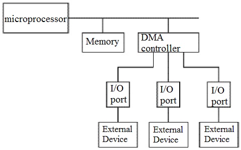
DMA controller provides an interface between the bus and the input-output devices. Although it transfers data without intervention of processor, it is controlled by the processor. The processor initiates the DMA controller by sending the starting address, Number of words in the data block and direction of transfer of data .i.e. from I/O devices to the memory or from main memory to I/O devices. More than one external device can be connected to the DMA controller.
DMA in Computer Architecture
DMA controller contains an address unit, for generating addresses and selecting I/O device for transfer. It also contains the control unit and data count for keeping counts of the number of blocks transferred and indicating the direction of transfer of data. When the transfer is completed, DMA informs the processor by raising an interrupt. The typical block diagram of the DMA controller is shown in the figure below.
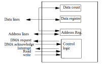
Typical Block Diagram of DMA Controller
Working of DMA Controller
DMA controller has to share the bus with the processor to make the data transfer. The device that holds the bus at a given time is called bus master. When a transfer from I/O device to the memory or vice versa has to be made, the processor stops the execution of the current program, increments the program counter, moves data over stack then sends a DMA select signal to DMA controller over the address bus.
If the DMA controller is free, it requests the control of bus from the processor by raising the bus request signal. Processor grants the bus to the controller by raising the bus grant signal, now DMA controller is the bus master. The processor initiates the DMA controller by sending the memory addresses, number of blocks of data to be transferred and direction of data transfer. After assigning the data transfer task to the DMA controller, instead of waiting ideally till completion of data transfer, the processor resumes the execution of the program after retrieving instructions from the stack.
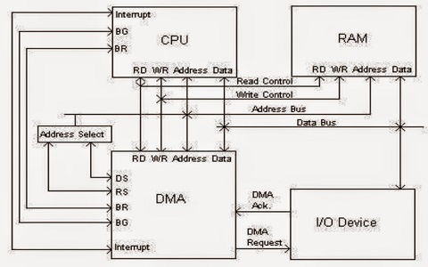
Transfer Of Data in Computer By DMA Controller
DMA controller now has the full control of buses and can interact directly with memory and I/O devices independent of CPU. It makes the data transfer according to the control instructions received by the processor. After completion of data transfer, it disables the bus request signal and CPU disables the bus grant signal thereby moving control of buses to the CPU.
When an I/O device wants to initiate the transfer then it sends a DMA request signal to the DMA controller, for which the controller acknowledges if it is free. Then the controller requests the processor for the bus, raising the bus request signal. After receiving the bus grant signal it transfers the data from the device. For n channeled DMA controller n number of external devices can be connected.
The DMA transfers the data in three modes which include the following.
a) Burst Mode: In this mode DMA handover the buses to CPU only after completion of whole data transfer. Meanwhile, if the CPU requires the bus it has to stay ideal and wait for data transfer.
b) Cycle Stealing Mode: In this mode, DMA gives control of buses to CPU after transfer of every byte. It continuously issues a request for bus control, makes the transfer of one byte and returns the bus. By this CPU doesn’t have to wait for a long time if it needs a bus for higher priority task.
c) Transparent Mode: Here, DMA transfers data only when CPU is executing the instruction which does not require the use of buses.
8237 DMA Controller
- 8237 has 4 I/O channels along with the flexibility of increasing the number of channels.
- Each channel can be programmed individually and has a 64k address and data capability.
- The timing control block, Program command control block, Priority Encoder Block are the three main blocks of 8237A.
- The internal timing and external control signals are driven by the timing control block.
- Various commands given by the microprocessor to the DMA are decoded by program command control block.
- Which channel has to be given the highest priority is decided by the priority encoder block.
8237A has 27 internal registers.
8237A operates in two cycles- Ideal cycle and active cycle, where each cycle contains 7 separate states composed of one clock period each.
S0- The first state, where the controller has requested for the bus and waiting for the acknowledgment from the processor.
S1, S2, S3, S4 are called the working states of the 8237A where the actual transfer of data takes place. If more time is needed for transfer wait states SW are added between these states.
For memory –to- memory transfer read-from-memory and write-to-memory transfers have to be made. Eight states are required for single transfer. The first four states with subscripts S11, S12, S13, S14 does the read-from-memory transfer and the next four S21, S22, S23, S24 are for write-to-memory transfer.
DMA goes into the ideal state when no channel is requesting service and perform SI state. SI is an inactive state where the DMA is inactive until it receives a request. In this state, DMA is in program condition where the processor can program the DMA.
When DMA is in the ideal state and gets no further channel requests, it outputs an HRQ signal to the processor and enters into Active state where it can start the transfer of data either by burst mode, cycle stealing mode or transparent mode.
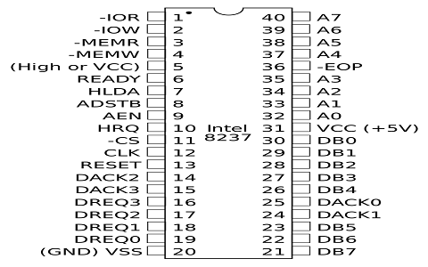
8237 Pin Diagram
8257 DMA Controller
When paired with single Intel 8212 I/O port device, the 8257 DMA controller forms a complete 4 channel DMA controller. Upon receiving a transfer request the 8257 controller-
- Acquires the control over system bus from the processor.
- The peripheral connected to the highest priority channel is acknowledged.
- The least significant bits of the memory address are moved over the address lines A0-A7 of the system bus.
- The most significant 8 bits of the memory address are driven to 8212 I/O port through data lines.
- Generates the appropriate controls signals for the transfer of data between peripherals and addressed memory locations.
- When the specified number of bytes are transferred, the controller informs the CPU end of transfer by activating the terminal count ( TC) output.
For each channel 8257 contains two 16-bit registers– 1) DMA address register and 2) Terminal count register, which should be initialized before a channel is enabled. The address of first memory location to be accessed is loaded in the DMA address register. The lower order 14 bits of the value loaded in the terminal count register indicates the number of DMA cycles minus one before the activation of Terminal count output. Type of operation for a channel is indicated by the most significant two bits of the Terminal count register.
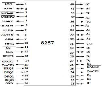
8257 Pin Diagram
Advantages and Disadvantages of DMA Controller
The advantages and disadvantages of DMA controller include the following.
Advantages
- DMA speedups the memory operations by bypassing the involvement of the CPU.
- The work overload on the CPU decreases.
- For each transfer, only a few numbers of clock cycles are required
Disadvantages
- Cache coherence problem can be seen when DMA is used for data transfer.
- Increases the price of the system.
DMA (Direct Memory Access) controller is being used in graphics cards, network cards, sound cards etc… DMA is also used for intra-chip transfer in multi-core processors. Operating in one of its three modes, DMA can considerably reduce the load of the processor
- A great number of devices on a bus will cause performance to suffer.
- Propagation delay : The time it takes for devices to coordinate the use of the bus.
- The bus may become a bottleneck as the aggregate data transfer demand approaches the capacity of the bus.
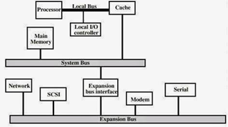
1)Traditional Hierarchi Bus Architecture
- Use of a cache structure insulates CPU from frequent accesses to main memory.
- Main memory can be moved off local bus t a system bus.
- Expansion bus interface buffers data transfers between system bus and I/O controllers on expansion.
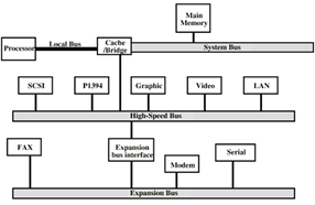
2) High-Performance Hierarchical Bus Architecture
- Incorporates a high-speed bus specifically designed to support high-capacity I/O devices.
- Bring high-demand devices into closer integration with processor.
The 8051 microcontrollers work with 8-bit data bus. So they can support external data memory up to 64K and external program memory of 64k at best. Collectively, 8051 microcontrollers can address 128k of external memory.
When data and code lie in different memory blocks, then the architecture is referred as Harvard architecture. In case data and code lie in the same memory block, then the architecture is referred as Von Neumann architecture.
Von Neumann Architecture
The Von Neumann architecture was first proposed by a computer scientist John von Neumann. In this architecture, one data path or bus exists for both instruction and data. As a result, the CPU does one operation at a time. It either fetches an instruction from memory, or performs read/write operation on data. So an instruction fetch and a data operation cannot occur simultaneously, sharing a common bus.
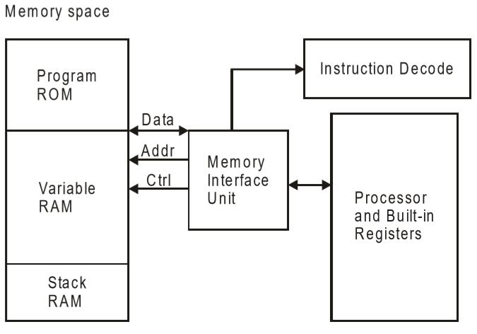
Von-Neumann architecture supports simple hardware. It allows the use of a single, sequential memory. Today's processing speeds vastly outpace memory access times, and we employ a very fast but small amount of memory (cache) local to the processor.
Harvard Architecture
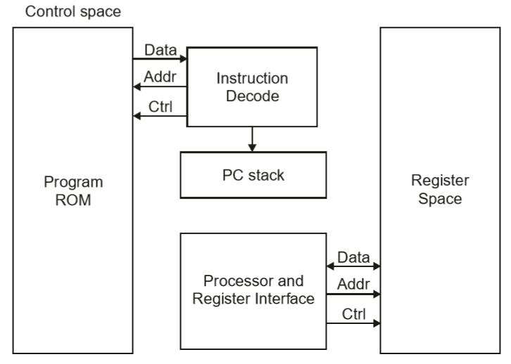
The Harvard architecture offers separate storage and signal buses for instructions and data. This architecture has data storage entirely contained within the CPU, and there is no access to the instruction storage as data. Computers have separate memory areas for program instructions and data using internal data buses, allowing simultaneous access to both instructions and data.
Programs needed to be loaded by an operator; the processor could not boot itself. In a Harvard architecture, there is no need to make the two memories share properties.
Von-Neumann Architecture vs Harvard Architecture
The following points distinguish the Von Neumann Architecture from the Harvard Architecture.
Von-Neumann Architecture | Harvard Architecture |
Single memory to be shared by both code and data. | Separate memories for code and data. |
Processor needs to fetch code in a separate clock cycle and data in another clock cycle. So it requires two clock cycles. | Single clock cycle is sufficient, as separate buses are used to access code and data. |
Higher speed, thus less time consuming. | Slower in speed, thus more time-consuming. |
Simple in design. | Complex in design. |
CISC and RISC
CISC is a Complex Instruction Set Computer. It is a computer that can address a large number of instructions.
In the early 1980s, computer designers recommended that computers should use fewer instructions with simple constructs so that they can be executed much faster within the CPU without having to use memory. Such computers are classified as Reduced Instruction Set Computer or RISC.
CISC vs RISC
The following points differentiate a CISC from a RISC −
CISC | RISC |
Larger set of instructions. Easy to program | Smaller set of Instructions. Difficult to program. |
Simpler design of compiler, considering larger set of instructions. | Complex design of compiler. |
Many addressing modes causing complex instruction formats. | Few addressing modes, fix instruction format. |
Instruction length is variable. | Instruction length varies. |
Higher clock cycles per second. | Low clock cycle per second. |
Emphasis is on hardware. | Emphasis is on software. |
Control unit implements large instruction set using micro-program unit. | Each instruction is to be executed by hardware. |
Slower execution, as instructions are to be read from memory and decoded by the decoder unit. | Faster execution, as each instruction is to be executed by hardware. |
Pipelining is not possible. | Pipelining of instructions is possible, considering single clock cycle. |
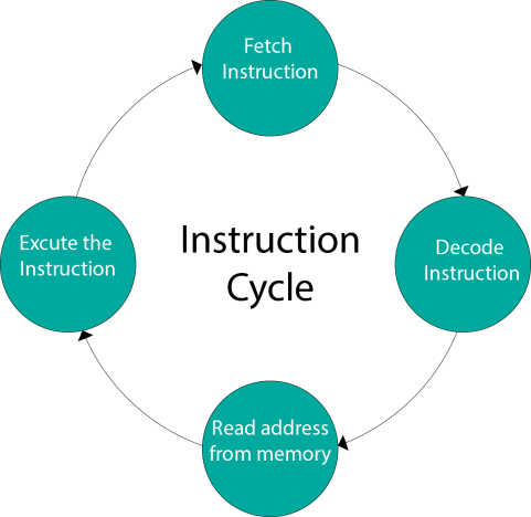
A program residing in the memory unit of a computer consists of a sequence of instructions. These instructions are executed by the processor by going through a cycle for each instruction.
In a basic computer, each instruction cycle consists of the following phases:
- Fetch instruction from memory.
- Decode the instruction.
- Read the effective address from memory.
- Execute the instruction.
Input-Output Configuration
In computer architecture, input-output devices act as an interface between the machine and the user.
Instructions and data stored in the memory must come from some input device. The results are displayed to the user through some output device.
The following block diagram shows the input-output configuration for a basic computer.
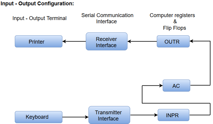
- The input-output terminals send and receive information.
- The amount of information transferred will always have eight bits of an alphanumeric code.
- The information generated through the keyboard is shifted into an input register 'INPR'.
- The information for the printer is stored in the output register 'OUTR'.
- Registers INPR and OUTR communicate with a communication interface serially and with the AC in parallel.
- The transmitter interface receives information from the keyboard and transmits it to INPR.
- The receiver interface receives information from OUTR and sends it to the printer serially.
Design of a Basic Computer
A basic computer consists of the following hardware components.
- A memory unit with 4096 words of 16 bits each
- Registers: AC (Accumulator), DR (Data register), AR (Address register), IR (Instruction register), PC (Program counter), TR (Temporary register), SC (Sequence Counter), INPR (Input register), and OUTR (Output register).
- Flip-Flops: I, S, E, R, IEN, FGI and FGO
Note: FGI and FGO are corresponding input and output flags which are considered as control flip-flops.
- Two decoders: a 3 x 8 operation decoder and 4 x 16 timing decoder
- A 16-bit common bus
- Control Logic Gates
- The Logic and Adder circuits connected to the input of AC.
Representing and storing numbers were the basic of operation of the computers of earlier times. The real go came when computation, manipulating numbers like adding, multiplying came into picture. These operations are handled by computer’s arithmetic logic unit (ALU). The ALU is the mathematical brain of a computer. The first ALU was INTEL 74181 implemented as a 7400 series is a TTL integrated circuit which was released in 1970.
The ALU is a digital circuit that provides arithmetic and logic operation. It is the fundamental building block of central processing unit of a computer. A modern CPU has very powerful ALU and it is complex in design. In addition to ALU modern CPU contains control unit and set of registers. Most of the operations are performed by one or more ALU’s, which load data from input register. Registers are a small amount of storage available to CPU. These registers can be accessed very fast. The control unit tells ALU what operation to perform on the available data. After calculation/manipulation the ALU stores the output in an output register.
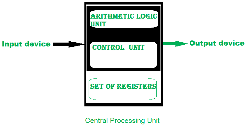
The CPU can be divided into two section: data section and control section. The DATA section is also known as data path.
BUS:
In early computers “BUS” were parallel electrical wires with multiple hardware connections. Therefore a bus is communication system that transfers data between component inside a computer, or between computers. It includes hardware components like wires, optical fibers, etc and software, including communication protocols. The Registers, ALU and the interconnecting BUS are collectively referred as data path.
Types of bus are:
- Address bus: The buses which are used to carry address.
- Data bus: The buses which are used to carry data.
- Control bus: If the bus is carrying control signals .
- Power bus: If it is carrying clock pulse, power signals it is known as power bus, and so on.
The bus can be dedicated, i.e., it can be used for a single purpose or it can be multiplexed, i.e., it can be used for multiple purpose. When we would have different kinds of buses, different types of bus organisation will take place.
- Program Counter –
A program counter (PC) is a CPU register in the computer processor which has the address of the next instruction to be executed from memory. As each instruction gets fetched, the program counter increases its stored value by 1. It is a digital counter needed for faster execution of tasks as well as for tracking the current execution point. - Instruction Register –
In computing, an instruction register (IR) is the part of a CPU’s control unit that holds the instruction currently being executed or decoded. An instruction register is the part of a CPU’s control unit that holds the instruction currently being executed or decoded. Instruction register specifically holds the instruction and provides it to instruction decoder circuit. - Memory Address Register –
The Memory Address Register (MAR) is the CPU register that either stores the memory address from which data will be fetched from the CPU, or the address to which data will be sent and stored. It is a temporary storage component in the CPU(central processing unit) which temporarily stores the address (location) of the data sent by the memory unit until the instruction for the particular data is executed. - Memory Data Register –
The memory data register (MDR) is the register in a computer’s processor, or central processing unit, CPU, that stores the data being transferred to and from the immediate access storage. Mmemory data register (MDR) is also known as memory buffer register (MBR). - General Purpose Register –
General purpose registers are used to store temporary data within the microprocessor. It is a multipurpose register. They can be used either by programmer or by a user.
One Bus organization –
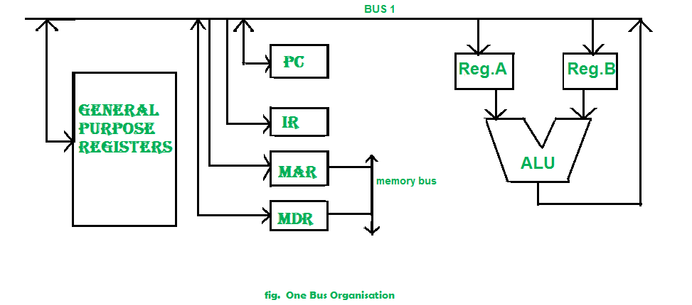
In one bus organisation, a single bus is used for multiple purpose. A set of general purpose register, program counter, instruction register, memory address register(MAR), memory data register(MDR) are connected with the single bus. Memory read/write can be done with MAR and MDR. The program counter points to the memory location from where the next instruction is to be fetched. Instruction register is that very register will hold the copy of the current instruction. In case of one bus organisation, at a time only one operand can be read from the bus.
As a result of that, if the requirement is to read two operand for the operation then read operation need to be carried twice. So that’s why it is making the process little longer. One of the advantage of one bus organisation is that, it is one of the simplest and also this is very cheap to implement. At the same time a disadvantage lies that it has only one bus and this “one bus” is accessed by all general purpose registers, program counter, instruction register, MAR, MDR making each and every operation sequential. No one recommend this architecture now-a-days.
Two Bus organization –
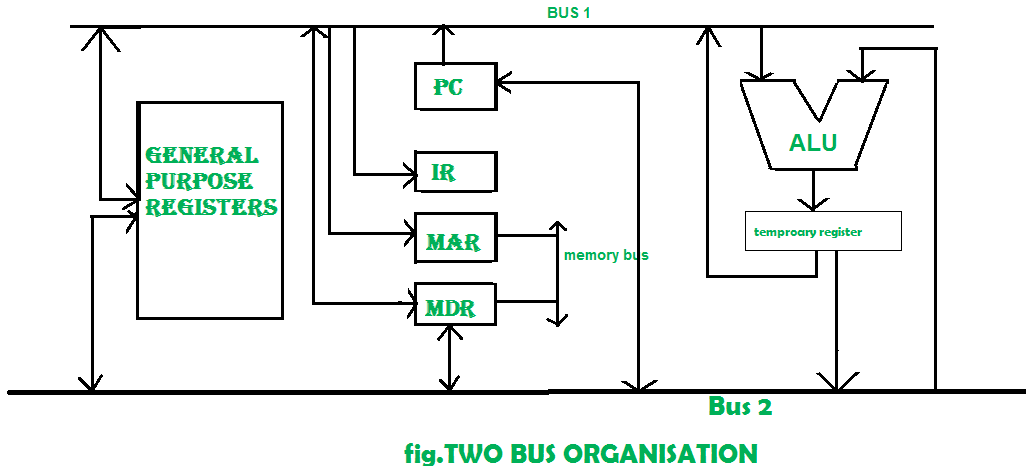
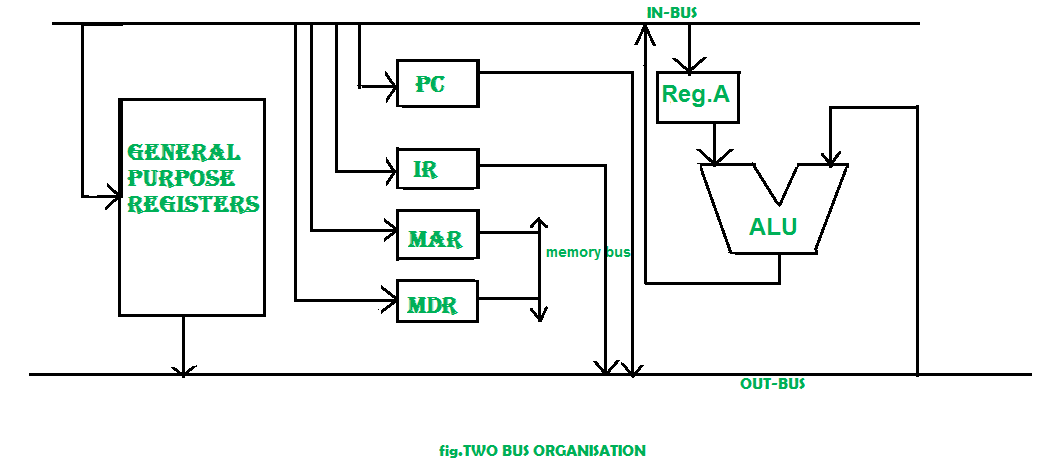
Two overcome the disadvantage of one bus organisation an another architecture was developed known as two bus organisation. In two bus organisation there are two buses. The general purpose register can read/write from both the buses. In this case, two operands can be fetched at the same time because of the two buses. One of bus fetch operand for ALU and another bus fetch for register. The situation arrises when both buses are busy fetching operands, output can be stored in temporary register and when the buses are free, particular output can be dumped on the buses.
There are two versions of two bus organisation, i.e., in-bus and out-bus.From in-bus the general purpose register can read data and to the out bus the general purpose registers can write data. Here buses gets dedicated.
Three Bus organization –
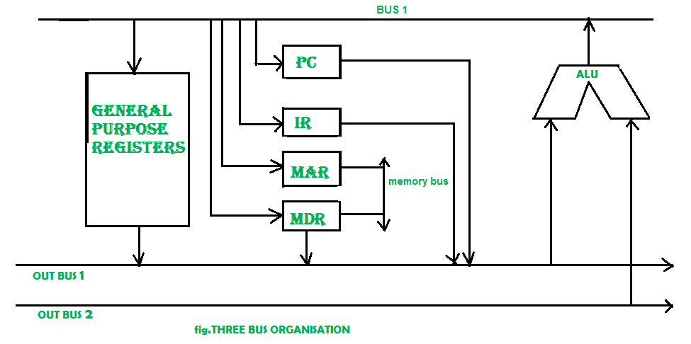
In three bus organisation we have three bus, OUT bus1, OUT bus2 and a IN bus. From the out buses we can get the operand which can come from general purpose register and evaluated in ALU and the output is dropped on In Bus so it can be sent to respective registers. This implementation is a bit complex but faster in nature because in parallel two operands can flow into ALU and out of ALU. It was developed to overcome the “busy waiting” problem of two bus organisation. In this structure after execution, the output can be dropped on the bus without waiting because of presence of an extra bus. The structure is given below in the figure.
The main advantages of multiple bus organisations over single bus are as given below.
- Increase in size of the registers.
- Reduction in the number of cycles for execution.
- Increases the speed of execution or we can say faster execution.
An arithmetic logic unit (ALU) is a digital electronic circuit present within the CPU that performs arithmetic and bitwise operations.
ALU deals with integer binary numbers while the floating point unit (FPU) deals with floating point numbers. ALU is a fundamental building block of many types of computing circuits like CPUs and GPUs.
A single CPU or GPU may also consist of more than one ALU. Moreover, input to the APU is the data to be operated called operand.
When the operation becomes more complex, then the ALU also becomes more expensive and takes up more space in the CPU and also produces more heat.
That’s why ALUs are powerful enough to ensure that the CPU fast but not so complex to become very expensive.
Arithmetic Logic Unit (ALU) Signals
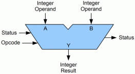
An Arithmetic Logic Unit (ALU) has a variety of input and output electrical connections that helps to convey digital signals between the ALU and external electronics.
External circuits give signals to the ALU input and in response, ALU outputs signal to external electronics.
Data:
ALU has three parallel buses consisting of two input operands and an output operand. The number of signals handled by all the three buses is the same.
Every data bus is a group of signals that conveys one binary integer number.
Opcode:
The opcode input is a parallel bus that transmits an operation selection code to the ALU. An operation selection code is a calculated value that specifies the desired arithmetic or logic operation that an ALU is going to perform.
The opcode size determines the greatest number of various operations the ALU can perform.
Status:
Output: The status outputs are many individual signals that convey supplemental data about the results of the ALU operations.
General ALUs usually have status signals such as: Carry out, zero, negative, overflow, etc. After the completion of each ALU operation, the status output signals were in external registers.
Storing these signals in registers makes them available for future ALU operations.
Input: The status inputs permit further information to access to the ALU once performing an operation. Moreover, this is a single “carry-in” bit that’s the stored carry-out from a previous ALU operation.
Arithmetic Logic Unit (ALU) Functions
Arithmetic Logic Units (ALU) has various numbers of basic arithmetic and bitwise logic functions. General purpose ALUs usually include these operations:
Arithmetic Operations: Arithmetic operations include addition and subtraction. However, sometimes multiplication and division are also used, these operations are more expensive to make.
That’s why multiplication and division are done by repetitive addition and subtraction. Some common arithmetic operations that an ALU performs are: add, subtract, increment, decrement, etc.
Bit shift operations: Bit shift operations cause operand to shift left or right. Simple ALUs can shift operands by only one-bit position, whereas more complex ALUs can shift by many bits.
Complex ALUs are able to shift by many bits because they have barrel shifters.
Bitwise Logical Operations: These are the operations like AND, OR, NOT, NOR, NAND, etc.
Register organization is the arrangement of the registers in the processor. The processor designers decide the organization of the registers in a processor. Different processors may have different register organization. Depending on the roles played by the registers they can be categorized into two types, user-visible register and control and status register.
Before learning register organization in brief, let us discuss what is register?
What is Register?
Registers are the smaller and the fastest accessible memory units in the central processing unit (CPU). According to memory hierarchy, the registers in the processor, function a level above the main memory and cache memory. The registers used by the central unit are also called as processor registers.
A register can hold the instruction, address location, or operands. Sometimes, the instruction has register as a part of itself.
Types of Registers
As we have discussed above, registers can be organized into two main categories i.e. the User-Visible Registers and the Control and Status Registers. Although we can’t separate the registers in the processors clearly among these two categories.
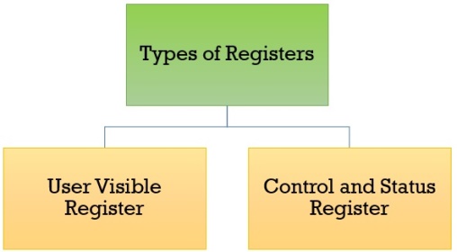
This is because in some processors, a register may be user-visible and in some, the same may not be user-visible. But for our rest of discussion regarding register organization, we will consider these two categories of register.
- User Visible Registers
- General Purpose Register
- Data Register
- Address Register
- Condition Codes
- Control and Status Registers
- Program Counter
- Instruction Register
- Memory Address Register
- Memory Buffer Register
User-Visible Registers
These registers are visible to the assembly or machine language programmers and they use them effectively to minimize the memory references in the instructions. Well, these registers can only be referenced using the machine or assembly language.

The registers that fall in this category are discussed below:
1. General Purpose Register
The general-purpose registers detain both the addresses or the data. Although we have separate data registers and address registers. The general purpose register also accepts the intermediate results in the course of program execution.
Well, the programmers can restrict some of the general-purpose registers to specific functions. Like, some registers are specifically used for stack operations or for floating-point operations. The general-purpose register can also be employed for the addressing functions.
2. Data Register
The term itself describes that these registers are employed to hold the data. But the programmers can’t use these registers for calculating operand address.
3. Address Register
Now, the address registers contain the address of an operand or it can also act as a general-purpose register. An address register may be dedicated to a certain addressing mode. Let us understand this with the examples.
(a) Segment Pointer Register
A memory divided in segments, requires a segment register to hold the base address of the segment. There can be multiple segment registers. As one segment register can be employed to hold the base address of the segment occupied by the operating system. The other segment register can hold the base address of the segment allotted to the processor.
(b) Index Register
The index register is employed for indexed addressing and it is initial value is 0. Generally, it used for traversing the memory locations. After each reference, the index register is incremented or decremented by 1, depending upon the nature of the operation.
Sometime the index register may be auto indexed.
(c) Stack Pointer Register
The stack register has the address that points the stack top.
4. Condition Code
Condition codes are the flag bits which are the part of the control register. The condition codes are set by the processor as a result of an operation and they are implicitly read through the machine instruction.
The programmers are not allowed to alter the conditional codes. Generally, the condition codes are tested during conditional branch operation.
Control and Status Registers
The control and status register holds the address or data that is important to control the processor’s operation. The most important thing is that these registers are not visible to the users. Below we will discuss all the control and status registers are essential for the execution of an instruction.

1. Program Counter
The program counter is a processor register that holds the address of the instruction that has to be executed next. It is a processor which updates the program counter with the address of the next instruction to be fetched for execution.
2. Instruction Register
Instruction register has the instruction that is currently fetched. It helps in analysing the opcode and operand present in the instruction.
3. Memory Address Register (MAR)
Memory address register holds the address of a memory location.
4. Memory Buffer Register (MBR)
The memory buffer register holds the data that has to be written to a memory location or it holds the data that is recently been read.
The memory address registers (MAR) and memory buffer registers (MBR) are used to move the data between processor and memory.
Apart from the above registers, several processors have a register termed as Program Status Word (PSW). As the word suggests it contains the status information.
The fields included in Program Status Word (PSW):
- Sign: This field has the resultant sign bit of the last arithmetic operation performed.
- Zero: This field is set when the result of the operation is zero.
- Carry: This field is set when an arithmetic operation results in a carry into or borrow out.
- Equal: If a logical operation results in, equality the Equal bit is set.
- Overflow: This bit indicates the arithmetic overflow.
- Interrupt: This bit is set to enable or disable the interrupts.
- Supervisor: This bit indicates whether the processor is executing in the supervisor mode or the user mode.
Control & status registers such as general purpose address registers, data registers
There are a variety of processor registers that are employed to control the operation of the processor. Most of these, on most machines, are not visible to the user. Some of them may be visible to machine instructions executed in a control or operating system mode.
Four registers are essential to instruction execution:
• Program counter (PC): Contains the address of an instruction to be fetched
• Instruction register (IR): Contains the instruction most recently fetched
• Memory address register (MAR): Contains the address of a location in memory
• Memory buffer register (MBR): Contains a word of data to be written to memory or the word most recently read
The four registers just mentioned are used for the movement of data between the processor and memory. Within the processor, data must be presented to the ALU for processing. The ALU may have direct access to the MBR and user-visible registers. Alternatively, there may be additional buffering registers at the boundary to the ALU; these registers serve as input and output registers for the ALU and exchange data with the MBR and user-visible registers.
Many processor designs include a register or set of registers, often known as the program status word (PSW), that contain status information. The PSW typically contains condition codes plus other status information. Common fields or flags include the following:
• Sign: Contains the sign bit of the result of the last arithmetic operation.
• Zero: Set when the result is 0.
• Carry: Set if an operation resulted in a carry (addition) into or borrow (subtraction) out of a high-order bit. Used for multiword arithmetic operations.
• Equal: Set if a logical compare result is equality.
• Overflow: Used to indicate arithmetic overflow.
• Interrupt Enable/Disable: Used to enable or disable interrupts.
• Supervisor: Indicates whether the processor is executing in supervisor or user mode. Certain privileged instructions can be executed only in supervisor mode, and certain areas of memory can be accessed only in supervisor mode.
Sample microprocessor register organizations are illustrated bellow.
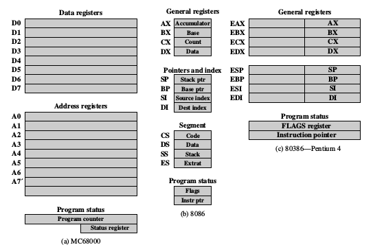
At higher levels of the hierarchy, memory is faster, smaller, and more expensive (per bit). Within the processor, there is a set of registers that function as a level of memory above main memory and cache in the hierarchy. The registers in the processor perform two roles:
• User-visible registers: Enable the machine- or assembly language programmer to minimize main memory references by optimizing use of registers.
• Control and status registers: Used by the control unit to control the operation of the processor and by privileged, operating system programs to control the execution of programs.
User-Visible Registers
A user-visible register is one that may be referenced by means of the machine language that the processor executes. We can characterize these in the following categories:
• General purpose
• Data
• Address
• Condition codes
General-purpose registers can be assigned to a variety of functions by the programmer. Sometimes their use within the instruction set is orthogonal to the operation. That is, any general-purpose register can contain the operand for any opcode. This provides true general-purpose register use. Often, however, there are restrictions. For example, there may be dedicated registers for floating-point and stack operations.
In some cases, general-purpose registers can be used for addressing functions (e.g., register indirect, displacement). In other cases, there is a partial or clean separation between data registers and address registers.
Data registers may be used only to hold data and cannot be employed in the calculation of an operand address.
Address registers may themselves be somewhat general purpose, or they may be devoted to a particular addressing mode. Examples include the following:
• Segment pointers: In a machine with segmented addressing, a segment register holds the address of the base of the segment. There may be multiple registers: for example, one for the operating system and one for the current process.
• Index registers: These are used for indexed addressing and may be autoindexed.
• Stack pointer: If there is user-visible stack addressing, then typically there is a dedicated register that points to the top of the stack. This allows implicit addressing; that is, push, pop, and other stack instructions need not contain an explicit stack operand.
A final category of registers, which is at least partially visible to the user, holds condition codes (also referred to as flags). Condition codes are bits set by the processor hardware as the result of operations. For example, an arithmetic operation may produce a positive, negative, zero, or overflow result. In addition to the result itself being stored in a register or memory, a condition code is also set. The code may subsequently be tested as part of a conditional branch operation. Condition code bits are collected into one or more registers. Usually, they form part of a control register. Generally, machine instructions allow these bits to be read by implicit reference, but the programmer cannot alter them.
Flags, PC, MAR, MBR, IR)
Registers Involved In Each Instruction Cycle:
- Memory address registers(MAR) : It is connected to the address lines of the system bus. It specifies the address in memory for a read or write operation.
- Memory Buffer Register(MBR) : It is connected to the data lines of the system bus. It contains the value to be stored in memory or the last value read from the memory.
- Program Counter(PC) : Holds the address of the next instruction to be fetched.
- Instruction Register(IR) : Holds the last instruction fetched.
The Instruction Cycle –
Each phase of Instruction Cycle can be decomposed into a sequence of elementary micro-operations. In the above examples, there is one sequence each for the Fetch, Indirect, Execute and Interrupt Cycles.
The Indirect Cycle is always followed by the Execute Cycle. The Interrupt Cycle is always followed by the Fetch Cycle. For both fetch and execute cycles, the next cycle depends on the state of the system.
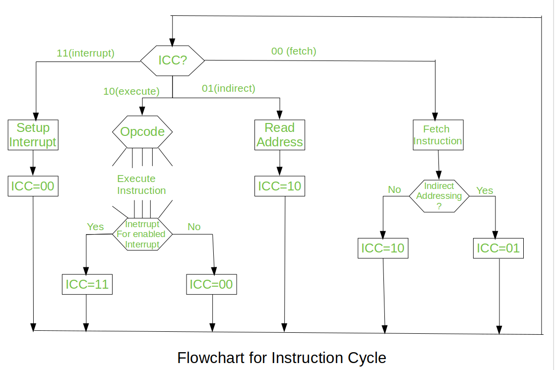
We assumed a new 2-bit register called Instruction Cycle Code (ICC). The ICC designates the state of processor in terms of which portion of the cycle it is in:-
00:Fetch Cycle
01:Indirect Cycle
10:Execute Cycle
11 : Interrupt Cycle
At the end of the each cycles, the ICC is set appropriately. The above flowchart of Instruction Cycle describes the complete sequence of micro-operations, depending only on the instruction sequence and the interrupt pattern(this is a simplified example). The operation of the processor is described as the performance of a sequence of micro-operation.
Different Instruction Cycles:
- The Fetch Cycle –
At the beginning of the fetch cycle, the address of the next instruction to be executed is in the Program Counter(PC).
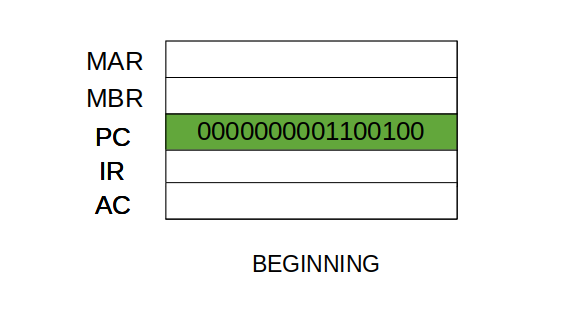
Step 1: The address in the program counter is moved to the memory address register(MAR), as this is the only register which is connected to address lines of the system bus.
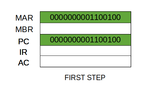
Step 2: The address in MAR is placed on the address bus, now the control unit issues a READ command on the control bus, and the result appears on the data bus and is then copied into the memory buffer register(MBR). Program counter is incremented by one, to get ready for the next instruction.(These two action can be performed simultaneously to save time)
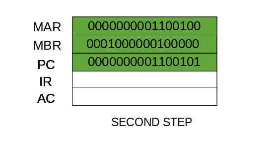
Step 3: The content of the MBR is moved to the instruction register(IR).
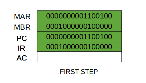
Thus, a simple Fetch Cycle consist of three steps and four micro-operation. Symbolically, we can write these sequence of events as follows:-
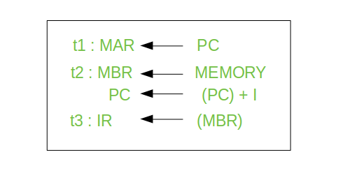
Here ‘I’ is the instruction length. The notations (t1, t2, t3) represents successive time units. We assume that a clock is available for timing purposes and it emits regularly spaced clock pulses. Each clock pulse defines a time unit. Thus, all time units are of equal duration. Each micro-operation can be performed within the time of a single time unit.
First time unit: Move the contents of the PC to MAR.
Second time unit: Move contents of memory location specified by MAR to MBR. Increment content of PC by I.
Third time unit: Move contents of MBR to IR.
Note: Second and third micro-operations both take place during the second time unit.
2. The Indirect Cycles –
Once an instruction is fetched, the next step is to fetch source operands. Source Operand is being fetched by indirect addressing( it can be fetched by any addressing mode, here its done by indirect addressing). Register-based operands need not be fetched. Once the opcode is executed, a similar process may be needed to store the result in main memory. Following micro-operations takes place:-
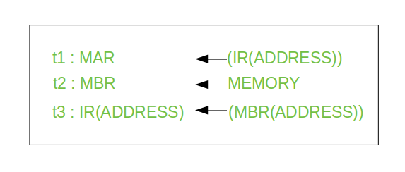
Step 1: The address field of the instruction is transferred to the MAR. This is used to fetch the address of the operand.
Step 2: The address field of the IR is updated from the MBR.(So that it now contains a direct addressing rather than indirect addressing)
Step 3: The IR is now in the state, as if indirect addressing has not been occurred.
Note: Now IR is ready for the execute cycle, but it skips that cycle for a moment to consider the Interrupt Cycle .
3. The Execute Cycle
The other three cycles(Fetch, Indirect and Interrupt) are simple and predictable. Each of them requires simple, small and fixed sequence of micro-operation. In each case same micro-operation are repeated each time around.
Execute Cycle is different from them. Like, for a machine with N different opcodes there are N different sequence of micro-operations that can occur.
Lets take an hypothetical example :-
consider an add instruction:
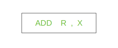
Here, this instruction adds the content of location X to register R. Corresponding micro-operation will be:-
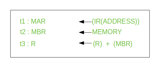
We begin with the IR containing the ADD instruction.
Step 1: The address portion of IR is loaded into the MAR.
Step 2: The address field of the IR is updated from the MBR, so the reference memory location is read.
Step 3: Now, the contents of R and MBR are added by the ALU.
Lets take a complex example :-

Here, the content of location X is incremented by 1. If the result is 0, the next instruction will be skipped. Corresponding sequence of micro-operation will be :-
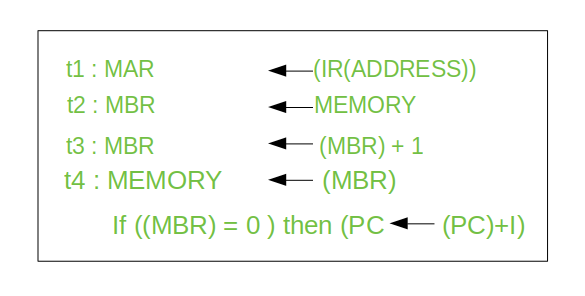
Here, the PC is incremented if (MBR) = 0. This test (is MBR equal to zero or not) and action (PC is incremented by 1) can be implemented as one micro-operation.
Note : This test and action micro-operation can be performed during the same time unit during which the updated value MBR is stored back to memory.
4. The Interrupt Cycle:
At the completion of the Execute Cycle, a test is made to determine whether any enabled interrupt has occurred or not. If an enabled interrupt has occurred then Interrupt Cycle occurs. The natare of this cycle varies greatly from one machine to another.
Lets take a sequence of micro-operation:-
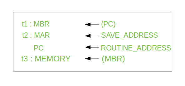
Step 1: Contents of the PC is transferred to the MBR, so that they can be saved for return.
Step 2: MAR is loaded with the address at which the contents of the PC are to be saved.
PC is loaded with the address of the start of the interrupt-processing routine.
Step 3: MBR, containing the old value of PC, is stored in memory.
Note: In step 2, two actions are implemented as one micro-operation. However, most processor provide multiple types of interrupts, it may take one or more micro-operation to obtain the save address and the routine address before they are transferred to the MAR and PC respectively.
Control unit (control signals & typical organization of hard wired & microprogrammed CU)
During the execution of a program, the control unit fetches one instruction at a time from the main memory and then executes it. In this execution process, it takes help of ALU, if the instruction execution involves arithmetic or logical operation (like AND, OR, Ex-OR). After execution of the current instruction, the CPU fetches the next instruction for execution. This process continues until the program is completed and the result is output using the output device. In many computers, the control unit and the ALU are integrated into a single block, known as Central Processing Unit (CPU).
Central Processing Unit (CPU) consists of the following features −
- CPU is considered as the brain of the computer.
- CPU performs all types of data processing operations.
- It stores data, intermediate results, and instructions (program).
- It controls the operation of all parts of the computer.
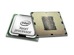
CPU itself has the following three components.
- Memory or Storage Unit
- a control unit
- ALU(Arithmetic Logic Unit)
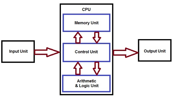
Memory or Storage Unit
This unit can store instructions, data, and intermediate results. This unit supplies information to other units of the computer when needed. It is also known as an internal storage unit or the main memory or the primary storage or Random Access Memory (RAM).
Its size affects speed, power, and capability. Primary memory and secondary memory are two types of memories in the computer. Functions of the memory unit are −
- It stores all the data and the instructions required for processing.
- It stores intermediate results of processing.
- It stores the final results of processing before these results are released to an output device.
- All inputs and outputs are transmitted through the main memory.
Control unit
This unit controls the operations of all parts of the computer but does not carry out any actual data processing operations.
Functions of this unit are −
- It is responsible for controlling the transfer of data and instructions among other units of a computer.
- It manages and coordinates all the units of the computer.
- It obtains the instructions from the memory, interprets them, and directs the operation of the computer.
- It communicates with Input/output devices for transfer of data or results from storage.
- It does not process or store data.
ALU (Arithmetic Logic Unit)
This unit consists of two subsections namely,
- Arithmetic section
- Logic Section
Arithmetic section
The function of arithmetic section is to perform arithmetic operations like addition, subtraction, multiplication, and division. All complex operations are done by making repetitive use of the above operations.
Logic Section
The function of the logic section is to perform logic operations such as comparing, selecting, matching, and merging of data.
The Control Unit is classified into two major categories:
- Hardwired Control
- Microprogrammed Control
Hardwired Control
The Hardwired Control organization involves the control logic to be implemented with gates, flip-flops, decoders, and other digital circuits.
The following image shows the block diagram of a Hardwired Control organization.
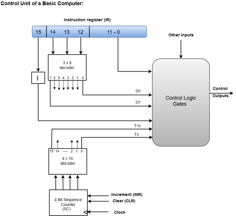
- A Hard-wired Control consists of two decoders, a sequence counter, and a number of logic gates.
- An instruction fetched from the memory unit is placed in the instruction register (IR).
- The component of an instruction register includes; I bit, the operation code, and bits 0 through 11.
- The operation code in bits 12 through 14 are coded with a 3 x 8 decoder.
- The outputs of the decoder are designated by the symbols D0 through D7.
- The operation code at bit 15 is transferred to a flip-flop designated by the symbol I.
- The operation codes from Bits 0 through 11 are applied to the control logic gates.
- The Sequence counter (SC) can count in binary from 0 through 15.
Micro-programmed Control
The Microprogrammed Control organization is implemented by using the programming approach.
In Microprogrammed Control, the micro-operations are performed by executing a program consisting of micro-instructions.
The following image shows the block diagram of a Microprogrammed Control organization.

- The Control memory address register specifies the address of the micro-instruction.
- The Control memory is assumed to be a ROM, within which all control information is permanently stored.
- The control register holds the microinstruction fetched from the memory.
- The micro-instruction contains a control word that specifies one or more micro-operations for the data processor.
- While the micro-operations are being executed, the next address is computed in the next address generator circuit and then transferred into the control address register to read the next microinstruction.
- The next address generator is often referred to as a micro-program sequencer, as it determines the address sequence that is read from control memory.
In computer central processing units, micro-operations (also known as micro-ops) are the functional or atomic, operations of a processor. These are low level instructions used in some designs to implement complex machine instructions. They generally perform operations on data stored in one or more registers. They transfer data between registers or between external buses of the CPU, also performs arithmetic and logical operations on registers.
In executing a program, operation of a computer consists of a sequence of instruction cycles, with one machine instruction per cycle. Each instruction cycle is made up of a number of smaller units – Fetch, Indirect, Execute and Interrupt cycles. Each of these cycles involves series of steps, each of which involves the processor registers. These steps are referred as micro-operations. The prefix micro refers to the fact that each of the step is very simple and accomplishes very little.
Figure below depicts constituent elements of a program execution.
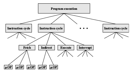
The Fetch Cycle
The fetch cycle occurs at the beginning of each in-]struction cycle and causes an instruction to be fetched from memory. Four registers are involved:
• Memory address register (MAR): Is connected to the address lines of the system bus. It specifies the address in memory for a read or write operation.
• Memory buffer register (MBR): Is connected to the data lines of the system bus. It contains the value to be stored in memory or the last value read from memory.
• Program counter (PC): Holds the address of the next instruction to be fetched.
• Instruction register (IR): Holds the last instruction fetched.
The simple fetch cycle actually consists of three steps and four micro operations. Each micro-operation involves the movement of data into or out of a register. So long as these movements do not interfere with one another, several of them can take place during one step, saving time. Symbolically, we can write this sequence of events as follows:
t 1 : MAR ← (PC)
t 2 : MBR ← Memory
PC ← (PC) + I
t 3 : IR ← (MBR)
Where I is the instruction length. We assume that a clock is available for timing purposes and that it emits regularly spaced clock pulses. Each clock pulse defines a time unit.Thus, all time units are of equal duration. Each micro-operation can be performed within the time of a single time unit. The notation (t 1 , t 2 , t 3 ) represents successive time units. In words, we have
• First time unit: Move contents of PC to MAR.
• Second time unit: Move contents of memory location specified by MAR to MBR. Increment by I the contents of the PC.
• Third time unit: Move contents of MBR to IR.
The second and third micro-operations both take place during the second time unit. The third micro-operation could have been grouped with the fourth withut affecting the fetch operation:
t 1 : MAR ← (PC)
t 2 : MBR ← Memory
t 3 : PC ← (PC) + I
IR ← (MBR)
The groupings of micro-operations must follow two simple rules:
1. The proper sequence of events must be followed. Thus (MAR ; (PC)) must precede (MBR ; Memory) because the memory read operation makes use of the address in the MAR.
2. Conflicts must be avoided. One should not attempt to read to and write from the same register in one time unit, because the results would be unpredictable. For example, the micro-operations (MBR ; Memory) and (IR ; MBR) should not occur during the same time unit.
The Indirect Cycle
Once an instruction is fetched, the next step is to fetch source operands. If the instruction specifies an indirect address, then an indirect cycle must precede the execute cycle. It includes the following micro-operations:
t 1 : MAR ← (IR(Address))
t 2 : MBR ← Memory
t 3 : IR(Address) ← (MBR(Address))
The address field of the instruction is transferred to the MAR. This is then used to fetch the address of the operand. Finally, the address field of the IR is updated from the MBR, so that it now contains a direct rather than an indirect address. The IR is now in the same state as if indirect addressing had not been used, and it is ready for the execute cycle. We skip that cycle for a moment, to consider the interrupt cycle.
The Interrupt Cycle
At the completion of the execute cycle, a test is made to determine whether any enabled interrupts have occurred. If so, the interrupt cycle occurs. The nature of this cycle varies greatly from one machine to another. We have the following sequence for the interrupt cycle.
t 1 : MBR ← (PC)
t 2 : MAR ← Save_Address
PC ← Routine_Address
t 3 : Memory ← (MBR)
In the first step, the contents of the PC are transferred to the MBR, so that they can be saved for return from the interrupt. Then the MAR is loaded with the address at which the contents of the PC are to be saved, and the PC is loaded with the address of the start of the interrupt-processing routine. These two actions may each be a single micro-operation. However, because most processors provide multiple types and/or levels of interrupts, it may take one or more additional micro-operations to obtain the Save_Address and the Routine_Address before they can be transferred to the MAR and PC, respectively. In any case, once this is done, the final step is to store the MBR, which contains the old value of the PC, into memory. The processor is now ready to begin the next instruction cycle.
The Execute Cycle
The fetch, indirect, and interrupt cycles are simple and predictable. Each involves a small, fixed sequence of micro-operations and, in each case, the same micro-operations
are repeated each time around. This is not true of the execute cycle. Because of the variety opcodes, there are a number of different sequences of micro-operations that can occur. Let us consider several hypothetical examples.
First, consider an add instruction:
ADD R1, X
which adds the contents of the location X to register R1. The following sequence of micro-operations might occur:
t 1 : MAR ← (IR(address))
t 2 : MBR ← Memory
t 3 : R1 ← (R1) + (MBR)
We begin with the IR containing the ADD instruction. In the first step, the address portion of the IR is loaded into the MAR. Then the referenced memory location is read. Finally, the contents of R1 and MBR are added by the ALU. Again, this is a simplified example. Additional micro-operations may be required to extract the register reference from the IR and perhaps to stage the ALU inputs or outputs in some intermediate registers.
Let us look at two more complex examples.
A common instruction is increment and skip if zero:
ISZ X
The content of location X is incremented by 1. If the result is 0, the next instruction is skipped. A possible sequence of micro-operations is,
t 1 : MAR ← (IR(address))
t 2 : MBR ← Memory
t 3 : MBR ← (MBR) + 1
t 4 : Memory ← (MBR)
If ((MBR) = 0) then (PC ← (PC) + I)
The new feature introduced here is the conditional action. The PC is incremented if (MBR) = 0. This test and action can be implemented as one micro-operation. Note also that this micro-operation can be performed during the same time unit during which the updated value in MBR is stored back to memory.
Finally, consider a subroutine call instruction. As an example, consider a branch-and-save-address instruction:
BSA X
The address of the instruction that follows the BSA instruction is saved in location X, and execution continues at location X + I. The saved address will later be used for return. This is a straightforward technique for providing subroutine calls. The following micro-operations suffice:
t 1 : MAR ← (IR(address))
MBR ← (PC)
t 2 : PC ← (IR(address))
Memory ← (MBR)
t 3 : PC ← (PC) + I
The address in the PC at the start of the instruction is the address of the next instruction in sequence. This is saved at the address designated in the IR. The latter address is also incremented to provide the address of the instruction for the next instruction cycle.
The Instruction Cycle
Figure below illustrates the flowchart for instruction cycle.
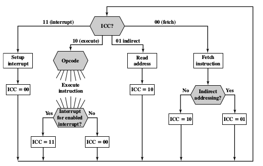
We assume a new 2-bit register called the instruction cycle code (ICC). The ICC designates the state of the processor in terms of which portion of the cycle it is in:
00: Fetch
01: Indirect
10: Execute
11: Interrupt
At the end of each of the four cycles, the ICC is set appropriately. The indirect cycle is always followed by the execute cycle. The interrupt cycle is always followed by the fetch cycle. For both the fetch and execute cycles, the next cycle depends on the state of the system.
Thus, the flowchart defines the complete sequence of micro operations, depending only on the instruction sequence and the interrupt pattern.
References:
1. “Digital Design”, M Morris Mano, Prentice Hall, Third Edition
2. “Computer organization” , Hamacher and Zaky, Fifth Edition
3. “Computer Organization and Design: The Hardware Software Interface” D. Patterson, J. Hennessy, Fourth Edition, Morgan Kaufmann
4. “ Microprocessors and interfacing-programming and hardware” Douglas V. Hall and SSSP Rao, McGraw-Hill ,Third Edition