Unit 6
Memory & Input / Output Systems
CHARACTERISTICS OF COMPUTER MEMORY SYSTEM
1) Location
- CPU registers
- Cache
- Internal Memory(main)
- External (secondary)
2) Capacity
- Word size : Typically equal to the number of bits used to represent a number and to the instruction length.
- For addresses of length A (in bits), the number of addressable units is 2^A.
3) Unit of Transfer
- Word
- Block
4) Access Method
* Sequential Access
- Access must be made in a specific linear sequence.
- Time to access an arbitrary record is highly variable.
* Direct access
- Individual blocks or record have an address based on physical location.
- Access is by direct access to general vicinity of desired information, then some search.
- Access time is still variable, but not as much as sequential access.
* Random access
- Each addressable location has a unique, physical location.
- Access is by direct access to desired location,
- Access time is constant and independent of prior accesses.
* Associative
- Desired units of information are retrieved by comparing a sub-part of unit.
- Location is needed.
- Most useful for searching.
5) Performance
* Access Time (Latency)
- For random access memory, latency is the time it takes to perform. A read or write operation that is the time from the instant that the address is presented to the memory to the instant that the data have been stored available for use.
* Memory Cycle Time
- Access time + additional time required before a second access can begin(refresh time, for example).
* Transfer Rate
- Generally measured in bit/second.
A memory unit is an essential component in any digital computer since it is needed for storing programs and data.
Typically, a memory unit can be classified into two categories:
- The memory unit that establishes direct communication with the CPU is called Main Memory. The main memory is often referred to as RAM (Random Access Memory).
- The memory units that provide backup storage are called Auxiliary Memory. For instance, magnetic disks and magnetic tapes are the most commonly used auxiliary memories.
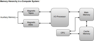
Apart from the basic classifications of a memory unit, the memory hierarchy consists all of the storage devices available in a computer system ranging from the slow but high-capacity auxiliary memory to relatively faster main memory.
The following image illustrates the components in a typical memory hierarchy.
Auxiliary Memory
Auxiliary memory is known as the lowest-cost, highest-capacity and slowest-access storage in a computer system. Auxiliary memory provides storage for programs and data that are kept for long-term storage or when not in immediate use. The most common examples of auxiliary memories are magnetic tapes and magnetic disks.
A magnetic disk is a digital computer memory that uses a magnetization process to write, rewrite and access data. For example, hard drives, zip disks, and floppy disks.
Magnetic tape is a storage medium that allows for data archiving, collection, and backup for different kinds of data.
Main Memory
The main memory in a computer system is often referred to as Random Access Memory (RAM). This memory unit communicates directly with the CPU and with auxiliary memory devices through an I/O processor.
The programs that are not currently required in the main memory are transferred into auxiliary memory to provide space for currently used programs and data.
I/O Processor
The primary function of an I/O Processor is to manage the data transfers between auxiliary memories and the main memory.
Cache Memory
The data or contents of the main memory that are used frequently by CPU are stored in the cache memory so that the processor can easily access that data in a shorter time. Whenever the CPU requires accessing memory, it first checks the required data into the cache memory. If the data is found in the cache memory, it is read from the fast memory. Otherwise, the CPU moves onto the main memory for the required data.
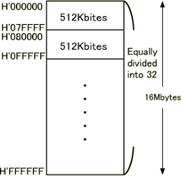
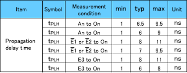
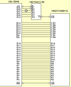
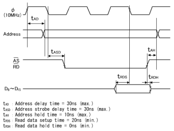
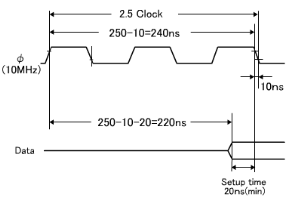
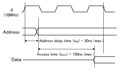
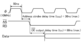
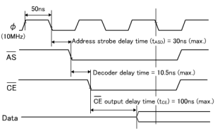
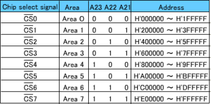
The following conditions are assumed here for connecting a CPU to a memory: |
|
|
|
|
|
|
|
|
|
Data are output from the memory only when all the access time, OE output delay time and CE output delay time requirements are satisfied.
| ||||||||||||||||||||||
The longest time for data to be output is 190.5ns due to the CE output delay time. As for the setup time, it causes no problem since the calculation results are 190.5ns (max.) against the requirement of 240ns (max.), providing an allowance of about 50ns.
|
|
|
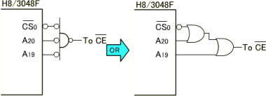 |
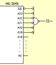
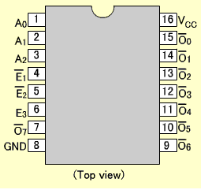
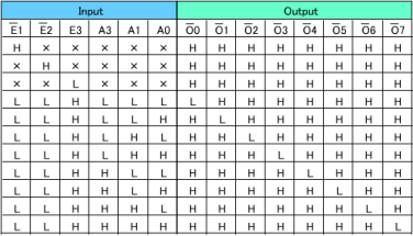
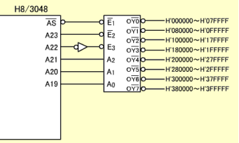
Figure: Decode Circuit Using CS0 |
A memory unit stores binary information in groups of bits called words. Data input lines provide the information to be stored into the memory, Data output lines carry the information out from the memory. The control lines Read and write specifies the direction of transfer of data. Basically, in the memory organization, there are  memory locations indexing from 0 to where l is the address buses. We can describe the memory in terms of the bytes using the following formula:
Where,
l is the total address buses
N is the memory in bytes
For example, some storage can be described below in terms of bytes using the above formula:
1kB= 210 Bytes
64 kB = 26 x 210 Bytes
= 216 Bytes
4 GB = 22 x 210(kB) x 210(MB) x 210 (GB)
= 232 Bytes
Memory Address Register (MAR) is the address register which is used to store the address of the memory location where the operation is being performed.
Memory Data Register (MDR) is the data register which is used to store the data on which the operation is being performed.
- Memory Read Operation:
Memory read operation transfers the desired word to address lines and activates the read control line. Description of memory read read operation is given below:
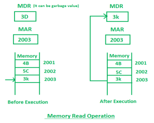
In the above diagram initially, MDR can contain any garbage value and MAR is containing 2003 memory address. After the execution of read instruction, the data of memory location 2003 will be read and the MDR will get updated by the value of the 2003 memory location (3D).
2. Memory Write Operation:
Memory write operation transfers the address of the desired word to the address lines, transfers the data bits to be stored in memory to the data input lines. Then it activates the write control line. Description of the write operation is given below:
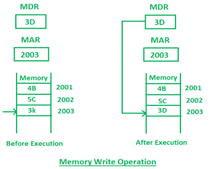
In the above diagram, the MAR contains 2003 and MDR contains 3D. After the execution of write instruction 3D will be written at 2003 memory location.
Key Characteristics of Computer Memory
The following expressed are the key characteristics of main computer memories.
- Semiconductor memory
A computer memory composed of a semiconductor is called a semiconductor memory, and the memory of the semiconductor is small in size, low in power, and short in access time. What’s more, when the power is lost, the stored data is also lost, which is a kind of volatile memory.
- Magnetic material memory
A computer memory made of magnetic material is called a magnetic memory. A layer of magnetic material is coated on metal or plastic to store data. The feature is that non-volatile, the data will not disappear after power-off, and the access speed is slow.
- Disk storage
The optical disk storage uses a laser to read on a magneto-optical material, which is non-volatility with good durability and high recording density. It is now used in computer systems as external storage.

RAM & ROM
Memory Terminology
Random Access Memory ( RAM )
The contents of the storage unit can be freely taken out or stored as needed. Such a memory will lose its storage contents when the power is turned off, therefore, it mainly used to store programs for short-term use. It is characterized by non-volatile, that is, power loss then memory loss.
There are two main types of RAM, one is called static RAM (SRAM). SRAM is very fast, in other words, it is the fastest storage device for reading and writing, but it is also very expensive. So it is only used in demanding places, the primary buffer or secondary buffer of CPU, for example. The other is called dynamic RAM (DRAM). DRAM keeps data for a short time and slower than SRAM, but it is faster than any ROM, but DRAM is cheaper than SRAM in terms of price. Many computers memory is DRAM.
SRAM (static random access memory) does not need to be refreshed when power is applied, that is, data will not lost, and is generally not multiplexed with row and column addresses. DRAM (dynamic random access memory) requires constant refresh to save data. Moreover, its row and column addresses are multiplexed, and many have page mode.
Read Only Memory ( ROM )
ROM usually refers to solidified computer memory (write once, read repeatedly), which is opposite to the RAM.
There are several categories of ROM. PROM is a programmable ROM, but it can be programmed once only, that is, after the software is written, it cannot be modified. This is an early product that is impossible to use nowadays.The EPROM, its original program is wiped out by ultraviolet light, is a general-purpose memory. Another type of EEPROM is electronically erased, which is expensive, has a long write time with very slow writing speed.
FLASH memory, combines the advantages of ROM and RAM, not only with the ability of electronic erasable programmable, but also does not loss data when power off and can quickly read data after power on. This memory is often used in U disk and MP3.
Currently, Flash has two main types, NOR Flash and NADN Flash. The reading of NOR Flash is the same as the common SDRAM. Users can directly run the code loaded in NOR FLASH, which can reduce the capacity of SRAM to save costs. NAND Flash does not take the read technology of internal memory. Its read is performed in the form of reading one block, usually 512 bytes at a time. In addition, users can't run the code directly on NAND Flash, so many manufacturers will give a small NOR Flash when produce a NAND Flash to run the boot code.
Generally, NOR Flash is used for small-capacity, because it has a fast reading speed and is used to store important information such as operating system. For large-capacity NAND flash, the most common application is disk on chip (DOC) used in embedded systems. And the "flash disk" we usually use, can be erased online.

Note
We can usually think that RAM is the data memory of the microcontroller (the data here includes internal data memory, usually user RAM area, bit addressable area, and work group register) and special function register SFR). ROM is the program memory of the MCU, and some MCUs may also include data memory. The data here refers to the data to be saved, that is, the data still existing after the MCU is powered off, in other words, the final collected data remained. The RAM only plays a role of saving data temporarily when the microcontroller is running. For example, some processing operations are performed on the collected data, so that an intermediate quantity is generated, and the RAM is used to temporarily access the intermediate quantity, and finally the result is placed in a ROM.
ROM can only read data from it under normal working conditions, and can't modify or rewrite data at any time. Its advantage is that the circuit structure is simple, and the data will not be lost after power off; the disadvantage is that it is only suitable for storing those fixed data. The fundamental difference between RAM and ROM is that RAM can write or read memory data at any time under normal operating conditions.
Volatile and Non-volatile Memory
- Static RAM ( SRAM )
It is a computer memory with a static access function that saves the data inside it without refreshing the circuit. Unlike DRAM memory, which needs to refresh the circuit, there is a need to charge and refresh the DRAM regularly, otherwise the internal storage data will disappear.
SRAM has higher performance, but SRAM also has its shortcoming, that is, its lower integration degree. Same-capacity DRAM memory can be designed to be smaller, but the SRAM requires a lot of size, thus the SRAM memory on the motherboard takes up a portion of the area.
Advantages: High speed, do not refresh circuit based on the memory characteristic , and the whole working efficiency can be improved.
Disadvantages: Low integration, large power consumption, and high price, but there is a small amount of it is used in key systems to improve efficiency.
- Dynamic RAM ( DRAM )
DRAM can only keep data for a short time. To maintain data, DRAM uses capacitor to store data, so it must be refreshed once in a while. If the memory unit is not refreshed, the stored information will be lost.
The memory of the computer we usually refer to is dynamic random access memory (DRAM). The so-called "dynamic" in here means that when we write data to DRAM, after a period of time, the data will be lost, so we need an additional circuit to perform a memory refresh operation. The specific working process is as follows: whether a DRAM memory cell stores 0 or 1 depends on whether the capacitor has a charge, having charge represents 1, and no charge represents 0.
However, for a long time, the capacitor representing 1 will discharge, and the capacitor representing 0 will absorb the charge. This is the cause of data loss. The regularly refresh operation is to check the capacitor: If the charge is greater than 1/2 of the full charge, it is considered to be 1 and fully charge the capacitor; if the charge is less than 1/2, it is considered to represent 0, and the capacitor is discharged.
Note
1) RAM
The structure of a DRAM memory cell is very simple, so it achieves a much higher level of integration than SRAM, but its access speed is not as fast as SRAM.
Synchronous Static RAM ( SSRAM ) and Synchronous Dynamic RAM ( SDRAM )
Synchronization means that the memory needs a clock, and the transmission of internal commands and data are based on it. Random means that the data is not stored in a linear order, but the data is read and written by the specified address. All accesses to the SSRAM are initiated on the rising/falling edge of the clock. Addresses, data inputs, and other control signals are all related to the clock signal. This is different from asynchronous SRAM, where access to it is independent of clock and data input and output are controlled by address changes.
2) ROM
MASK ROM
A mask read-only memory is a manufacturer that prepares a ROM or EPROM with raw data as a sample in advance for mass production, and then mass-produces the same ROM as the sample. This is a mass production. The ROM sample is the MASK ROM, and the data burned in the MASK ROM can never be modified.
One-time Programmable ROM ( OTP ROM )
Programmable ROM: once the content has been written, it is impossible to modify, so it can only be written once.
Erasable programmable ROM: erased with ultraviolet light, written with high voltage programming ( +21V or +12V ).
Electrically Erasable Programmable ROM (EEPROM) is used for electrical signal erasure.
Electrical signal can be erased.

Differences between MASK ROM,FALSH ROM and OTP ROM
The program of MASK ROM is solidified at the factory, and suitable for applications where the program is fixed; FALSH ROM's program can be erased repeatedly, with great flexibility, but at a higher price, and suitable for price-insensitive applications or development purposes; OTP ROM price is between the MASK ROM and FALSH ROM, and can be programmed once, therefore, it is suitable for applications that require both flexibility and low cost, especially for electronic products that need continuous refurbishment and meet rapid mass production.
The commonality between OTP ROM and PROM is that they can only be programmed once.
DDR: Double Date Rate. A common DDR SDRAM refers to a double rate synchronous dynamic random access memory.
The difference between DDR SDRAM and SDRAM: SDRAM transfers data only once in one clock cycle, and it transmits data during the rising period of the clock; while DDR memory transmits data twice in one clock cycle of each period. Also it can achieve higher data rates at the same bus frequency as SDRAM.
Note: Why DDR3 can replace DDR2 memory?
Frequency: DDR3 can operate from 800MHz to 1666MHz or more; while DDR2 operates from 533MHz to 1066MHz. In general, DDR3 is twice the frequency of DDR2, and the operating performance is improved by reducing the read and write time by half.
Power consumption: DDR3 can save 16% of energy compared to DDR2, because the new generation of DDR3 operates at 1.5V, while DDR2 operates at 1.8V, which can compensate for the high power generated by excessive operating frequency. At the same time, less energy consumption can extend the life of the component.
Technology: DDR3 memory bank has increased to eight, double the DDR2. So compared to DDR2 pre-read, it will increase efficiency by 50%, which is twice the DDR2 standard.
Main Technical Indicators of Computer Memory
Storage capacity: It generally refers to the number of storage units (N) included in a memory.
Access time (TA): It refers to the memory from the acceptance of the command to the read ∕ write data and stabilizes at the data register (MDP) output.
Memory cycle time (TMC): The minimum time required between two independent access operations, in addition, TMC is usually longer than TA.
Access rate: The total number of bits of information exchanged between main memory and the outside (such as CPU) per unit time.
Reliability: It described by the mean time between failures (MTBF), that is, the average interval time between two failures.
Locality of reference refers to a phenomenon in which a computer program tends to access same set of memory locations for a particular time period. In other words, Locality of Reference refers to the tendency of the computer program to access instructions whose addresses are near one another. The property of locality of reference is mainly shown by loops and subroutine calls in a program.
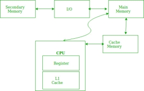
- In case of loops in program control processing unit repeatedly refers to the set of instructions that constitute the loop.
- In case of subroutine calls, everytime the set of instructions are fetched from memory.
- References to data items also get localized that means same data item is referenced again and again.

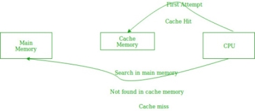
In the above figure, you can see that the CPU wants to read or fetch the data or instruction. First, it will access the cache memory as it is near to it and provides very fast access. If the required data or instruction is found, it will be fetched. This situation is known as a cache hit. But if the required data or instruction is not found in the cache memory then this situation is known as a cache miss. Now the main memory will be searched for the required data or instruction that was being searched and if found will go through one of the two ways:
- First way is that the CPU should fetch the required data or instruction and use it and that’s it but what, when the same data or instruction is required again. CPU again has to access the same main memory location for it and we already know that main memory is the slowest to access.
- The second way is to store the data or instruction in the cache memory so that if it is needed soon again in the near future it could be fetched in a much faster way.
Cache Operation:
It is based on the principle of locality of reference. There are two ways with which data or instruction is fetched from main memory and get stored in cache memory. These two ways are the following:
- Temporal Locality –
Temporal locality means current data or instruction that is being fetched may be needed soon. So we should store that data or instruction in the cache memory so that we can avoid again searching in main memory for the same data.
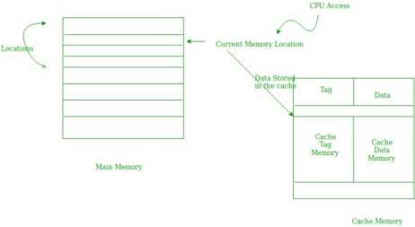
When CPU accesses the current main memory location for reading required data or instruction, it also gets stored in the cache memory which is based on the fact that same data or instruction may be needed in near future. This is known as temporal locality. If some data is referenced, then there is a high probability that it will be referenced again in the near future.
2. Spatial Locality –
Spatial locality means instruction or data near to the current memory location that is being fetched, may be needed soon in the near future. This is slightly different from the temporal locality. Here we are talking about nearly located memory locations while in temporal locality we were talking about the actual memory location that was being fetched.
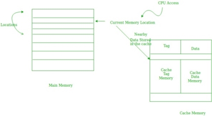
Cache Performance:
The performance of the cache is measured in terms of hit ratio. When CPU refers to memory and find the data or instruction within the Cache memory, it is known as cache hit. If the desired data or instruction is not found in the cache memory and CPU refers to the main memory to find that data or instruction, it is known as a cache miss.
Hit + Miss = Total CPU Reference
Hit Ratio(h) = Hit / (Hit+Miss)
Average access time of any memory system consists of two levels: Cache and Main Memory. If Tc is time to access cache memory and Tm is the time to access main memory then we can write:
Tavg = Average time to access memory
Tavg = h * Tc + (1-h)*(Tm + Tc)
In a computer
- Memory is organized at different levels.
- CPU may try to access different levels of memory in different ways.
- On this basis, the memory organization is broadly divided into two types-

- Simultaneous Access Memory Organization
- Hierarchical Access Memory Organization
1. Simultaneous Access Memory Organization-
In this memory organization,
- All the levels of memory are directly connected to the CPU.
- Whenever CPU requires any word, it starts searching for it in all the levels simultaneously.
Example-01:
Consider the following simultaneous access memory organization-
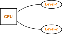
Here, two levels of memory are directly connected to the CPU.
Let-
- T1 = Access time of level L1
- S1 = Size of level L1
- C1 = Cost per byte of level L1
- H1 = Hit rate of level L1
Similar are the notations for level L2.
Average Memory Access Time-
Average time required to access memory per operation
= H1 x T1 + (1 – H1) x H2 x T2
= H1 x T1 + (1 – H1) x 1 x T2
= H1 x T1 + (1 – H1) x T2
Important Note
In any memory organization,
- The data item being searched will definitely be present in the last level.
- Thus, hit rate for the last level is always 1.
Average Cost Per Byte-
Average cost per byte of the memory
= { C1 x S1 + C2 x S2 } / { S1 + S2 }
Example-02:
Consider the following simultaneous access memory organization-
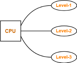
Here, three levels of memory are directly connected to the CPU.
Let-
- T1 = Access time of level L1
- S1 = Size of level L1
- C1 = Cost per byte of level L1
- H1 = Hit rate of level L1
Similar are the notations for other two levels.
Average Memory Access Time-
Average time required to access memory per operation
= H1 x T1 + (1 – H1) x H2 x T2 + (1 – H1) x (1 – H2) x H3 x T3
= H1 x T1 + (1 – H1) x H2 x T2 + (1 – H1) x (1 – H2) x 1 x T3
= H1 x T1 + (1 – H1) x H2 x T2 + (1 – H1) x (1 – H2) x T3
Average Cost Per Byte-
Average cost per byte of the memory
= { C1 x S1 + C2 x S2 + C3 x S3 } / { S1 + S2 + S3 }
2. Hierarchical Access Memory Organization-
In this memory organization, memory levels are organized as-
- Level-1 is directly connected to the CPU.
- Level-2 is directly connected to level-1.
- Level-3 is directly connected to level-2 and so on.
Whenever CPU requires any word,
- It first searches for the word in level-1.
- If the required word is not found in level-1, it searches for the word in level-2.
- If the required word is not found in level-2, it searches for the word in level-3 and so on.
Example-01:
Consider the following hierarchical access memory organization-
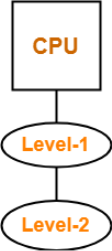
Here, two levels of memory are connected to the CPU in a hierarchical fashion.
Let-
- T1 = Access time of level L1
- S1 = Size of level L1
- C1 = Cost per byte of level L1
- H1 = Hit rate of level L1
Similar are the notations for level L2.
Average Memory Access Time-
Average time required to access memory per operation
= H1 x T1 + (1 – H1) x H2 x (T1 + T2)
= H1 x T1 + (1 – H1) x 1 x (T1 + T2)
= H1 x T1 + (1 – H1) x (T1 + T2)
Average Cost Per Byte-
Average cost per byte of the memory
= { C1 x S1 + C2 x S2 } / { S1 + S2 }
Example-02:
Consider the following hierarchical access memory organization-

Here, three levels of memory are connected to the CPU in a hierarchical fashion.
Let-
- T1 = Access time of level L1
- S1 = Size of level L1
- C1 = Cost per byte of level L1
- H1 = Hit rate of level L1
Similar are the notations for other two levels.
Average Memory Access Time-
Average time required to access memory per operation
= H1 x T1 + (1 – H1) x H2 x (T1 + T2) + (1 – H1) x (1 – H2) x H3 x (T1 + T2 + T3)
= H1 x T1 + (1 – H1) x H2 x (T1 + T2) + (1 – H1) x (1 – H2) x 1 x (T1 + T2 + T3)
= H1 x T1 + (1 – H1) x H2 x (T1 + T2) + (1 – H1) x (1 – H2) x (T1 + T2 + T3)
Average Cost Per Byte-
Average cost per byte of the memory
= { C1 x S1 + C2 x S2 + C3 x S3 } / { S1 + S2 + S3 }
PRACTICE PROBLEMS BASED ON MEMORY ORGANIZATION-
Problem-01:
What is the average memory access time for a machine with a cache hit rate of 80% and cache access time of 5 ns and main memory access time of 100 ns when-
- Simultaneous access memory organization is used.
- Hierarchical access memory organization is used.
Solution-
Part-01: Simultaneous Access Memory Organization-
The memory organization will be as shown-
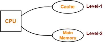
Average memory access time
= H1 x T1 + (1 – H1) x H2 x T2
= 0.8 x 5 ns + (1 – 0.8) x 1 x 100 ns
= 4 ns + 0.2 x 100 ns
= 4 ns + 20 ns
= 24 ns
Part-02: Hierarchical Access Memory Organization-
The memory organization will be as shown-
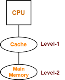
Average memory access time
= H1 x T1 + (1 – H1) x H2 x (T1 + T2)
= 0.8 x 5 ns + (1 – 0.8) x 1 x (5 ns + 100 ns)
= 4 ns + 0.2 x 10⁵ ns
= 4 ns + 21 ns
= 25 ns
Problem-02:
A computer has a cache, main memory and a disk used for virtual memory. An access to the cache takes 10 ns. An access to main memory takes 100 ns. An access to the disk takes 10,000 ns. Suppose the cache hit ratio is 0.9 and the main memory hit ratio is 0.8. The effective access time required to access a referenced word on the system is _______ when-
- Simultaneous access memory organization is used.
- Hierarchical access memory organization is used.
Solution-
Part-01:Simultaneous Access Memory Organization-
The memory organization will be as shown-
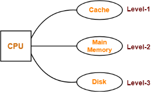
Effective memory access time
= H1 x T1 + (1 – H1) x H2 x T2 + (1 – H1) x (1 – H2) x H3 x T3
= 0.9 x 10 ns + (1 – 0.9) x 0.8 x 100 ns + (1 – 0.9) x (1 – 0.8) x 1 x 10000 ns
= 9 ns + 8 ns + 200 ns
= 217 ns
Part-02: Hierarchical Access Memory Organization-
The memory organization will be as shown-
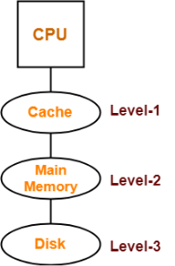
Effective memory access time
= H1 x T1 + (1 – H1) x H2 x (T1 + T2) + (1 – H1) x (1 – H2) x H3 x (T1 + T2 + T3)
= 0.9 x 10 ns + (1 – 0.9) x 0.8 x (10 ns + 100 ns) + (1 – 0.9) x (1 – 0.8) x 1 x (10 ns + 100 ns + 10000 ns)
= 9 ns + 8.8 ns + 202.2 ns
= 220 ns
Cache memory bridges the speed mismatch between the processor and the main memory.
When cache hit occurs,
- The required word is present in the cache memory.
- The required word is delivered to the CPU from the cache memory.
When cache miss occurs,
- The required word is not present in the cache memory.
- The page containing the required word has to be mapped from the main memory.
- This mapping is performed using cache mapping techniques.
Cache Mapping-
- Cache mapping defines how a block from the main memory is mapped to the cache memory in case of a cache miss.
OR
- Cache mapping is a technique by which the contents of main memory are brought into the cache memory.
The following diagram illustrates the mapping process-
Now, before proceeding further, it is important to note the following points-
NOTES
- Main memory is divided into equal size partitions called as blocks or frames.
- Cache memory is divided into partitions having same size as that of blocks called as lines.
During cache mapping, block of main memory is simply copied to the cache and the block is not actually brought from the main memory.
Cache Mapping Techniques-
Cache mapping is performed using following three different techniques-

- Direct Mapping
- Fully Associative Mapping
- K-way Set Associative Mapping
1. Direct Mapping-
In direct mapping,
- A particular block of main memory can map only to a particular line of the cache.
- The line number of cache to which a particular block can map is given by-
Cache line number
= ( Main Memory Block Address ) Modulo (Number of lines in Cache)
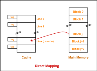
Example-
- Consider cache memory is divided into ‘n’ number of lines.
- Then, block ‘j’ of main memory can map to line number (j mod n) only of the cache.
Need of Replacement Algorithm-
In direct mapping,
- There is no need of any replacement algorithm.
- This is because a main memory block can map only to a particular line of the cache.
- Thus, the new incoming block will always replace the existing block (if any) in that particular line.
Division of Physical Address-
In direct mapping, the physical address is divided as-
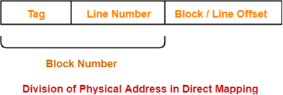
2. Fully Associative Mapping-
In fully associative mapping,
- A block of main memory can map to any line of the cache that is freely available at that moment.
- This makes fully associative mapping more flexible than direct mapping.
Example-
Consider the following scenario-
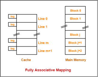
Here,
- All the lines of cache are freely available.
- Thus, any block of main memory can map to any line of the cache.
- Had all the cache lines been occupied, then one of the existing blocks will have to be replaced.
Need of Replacement Algorithm-
In fully associative mapping,
- A replacement algorithm is required.
- Replacement algorithm suggests the block to be replaced if all the cache lines are occupied.
- Thus, replacement algorithm like FCFS Algorithm, LRU Algorithm etc is employed.
Division of Physical Address-
In fully associative mapping, the physical address is divided as-

3. K-way Set Associative Mapping-
In k-way set associative mapping,
- Cache lines are grouped into sets where each set contains k number of lines.
- A particular block of main memory can map to only one particular set of the cache.
- However, within that set, the memory block can map any cache line that is freely available.
- The set of the cache to which a particular block of the main memory can map is given by-
Cache set number
= ( Main Memory Block Address ) Modulo (Number of sets in Cache)
Example-
Consider the following example of 2-way set associative mapping-
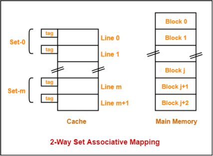
Here,
- k = 2 suggests that each set contains two cache lines.
- Since cache contains 6 lines, so number of sets in the cache = 6 / 2 = 3 sets.
- Block ‘j’ of main memory can map to set number (j mod 3) only of the cache.
- Within that set, block ‘j’ can map to any cache line that is freely available at that moment.
- If all the cache lines are occupied, then one of the existing blocks will have to be replaced.
Need of Replacement Algorithm-
- Set associative mapping is a combination of direct mapping and fully associative mapping.
- It uses fully associative mapping within each set.
- Thus, set associative mapping requires a replacement algorithm.
Division of Physical Address-
In set associative mapping, the physical address is divided as-

Special Cases-
If k = 1, then k-way set associative mapping becomes direct mapping i.e.
1-way Set Associative Mapping ≡ Direct Mapping
If k = Total number of lines in the cache, then k-way set associative mapping becomes fully associative mapping.
Normally we can perform both read operation and write operation on the cache memory.
Now when we perform read operation on cache memory then it does not change the content of the memory. But as it is obvious that any write operation performed on the cache changes the content of the memory. Thus it is important to perform any write on cache very carefully.
To make sure write operation is performed carefully; we can adopt two cache write methods:
- Write-through policy
- Write-back policy
Let’s learn about above two cache write methods in computer architecture.
Write-through policy
Write-through policy is the most commonly used methods of writing into the cache memory.
In write-through method when the cache memory is updated simultaneously the main memory is also updated. Thus at any given time, the main memory contains the same data which is available in the cache memory.
It is to be noted that, write-through technique is a slow process as every time it needs to access main memory.
Write-back policy
Write-back policy can also be used for cache writing.
During a write operation only the cache location is updated while following write-back method. When update in cache occurs then updated location is marked by a flag. The flag is known as modified or dirty bit.
When the word is replaced from the cache, it is written into main memory if its flag bit is set. The logic behind this technique is based on the fact that during a cache write operation, the word present in the cache may be accessed several times (temporal locality of reference). This method helps reduce the number of references to main memory.
The only limitation to write-back technique is that inconsistency may occur while adopting this technique due to two different copies of the same data, one in cache and other in main memory.
When a MM block needs to be brought in while all the CM blocks are occupied, one of them has to be replaced. The selection of this block to be replaced can be determined in one of the following ways.
- Optimal Replacement: replace the block which is no longer needed in the future. If all blocks currently in CM will be used again, replace the one which will not be used in the future for the longest time.
- Random selection: replace a randomly selected block among all blocks currently in CM.
- FIFO (first-in first-out): replace the block that has been in CM for the longest time.
- LRU: replace the block in CM that has not been used for the longest time, i.e., the least recently used (LRU) block.
The optimal replacement is obviously the best but is not realistic, simply because when a block will be needed in the future is usually not known ahead of time. The LRU is suboptimal based on the temporal locality of reference, i.e., memory items that are recently referenced are more likely to be referenced soon than those which have not been referenced for a longer time. FIFO is not necessarily consistent with LRU therefore is usually not as good. The radom selection, surprisingly, is not necessarily bad.
LRU replacement can be implemented by attaching a number to each CM block to iidicate how recent a block has been used. Eveytime a CPU reference is made all of these numbers are updated in such a way that the smaller a number the more recent it was used, i.e., the LRU block is always indicated by the largest number.
- Block needed: set the number to zero:

In case of a miss, bring the block needed in (replace an existing CM block if necessary)
- Other blocks in CM:

Example:
Assume the initial state of the 4 CM blocks is shown below (the underlined block is the least recently used):

After block B is referenced,

After block C is referenced,

After block D is referenced,

If block E not currently in CM is needed, the LRU CM block A labeled by the largest number 3 will be replaced

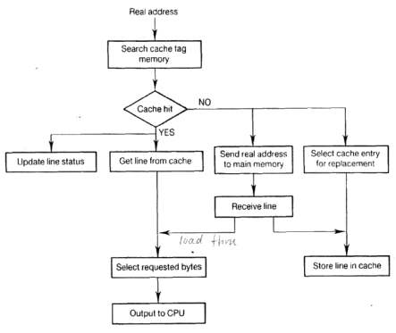
Cache is a random access memory used by the CPU to reduce the average time taken to access memory.
Multilevel Caches is one of the techniques to improve Cache Performance by reducing the “MISS PENALTY”. Miss Penalty refers to the extra time required to bring the data into cache from the Main memory whenever there is a “miss” in cache .
For clear understanding let us consider an example where CPU requires 10 Memory References for accessing the desired information and consider this scenario in the following 3 cases of System design :
Case 1 : System Design without Cache Memory

Here the CPU directly communicates with the main memory and no caches are involved.
In this case, the CPU needs to access the main memory 10 times to access the desired information.
Case 2 : System Design with Cache Memory

Here the CPU at first checks whether the desired data is present in the Cache Memory or not i.e. whether there is a “hit” in cache or “miss” in cache. Suppose there are 3 miss in Cache Memory then the Main Memory will be accessed only 3 times. We can see that here the miss penalty is reduced because the Main Memory is accessed a lesser number of times than that in the previous case.
Case 3 : System Design with Multilevel Cache Memory

Here the Cache performance is optimized further by introducing multilevel Caches. As shown in the above figure, we are considering 2 level Cache Design. Suppose there are 3 miss in the L1 Cache Memory and out of these 3 misses there are 2 miss in the L2 Cache Memory then the Main Memory will be accessed only 2 times. It is clear that here the Miss Penalty is reduced considerably than that in the previous case thereby improving the Performance of Cache Memory.
NOTE :
We can observe from the above 3 cases that we are trying to decrease the number of Main Memory References and thus decreasing the Miss Penalty in order to improve the overall System Performance. Also, it is important to note that in the Multilevel Cache Design, L1 Cache is attached to the CPU and it is small in size but fast. Although, L2 Cache is attached to the Primary Cache i.e. L1 Cache and it is larger in size and slower but still faster than the Main Memory.
Effective Access Time = Hit rate * Cache access time
+ Miss rate * Lower level access time
Average access Time For Multilevel Cache:(Tavg)
Tavg = H1 * C1 + (1 – H1) * (H2 * C2 +(1 – H2) *M )
Where
H1 is the Hit rate in the L1 caches.
H2 is the Hit rate in the L2 cache.
C1 is the Time to access information in the L1 caches.
C2 is the Miss penalty to transfer information from the L2 cache to an L1 cache.
M is the Miss penalty to transfer information from the main memory to the L2 cache.
Example:
Find the Average memory access time for a processor with a 2 ns clock cycle time, a miss rate of 0.04 misses per instruction, a miss penalty of 25 clock cycles, and a cache access time (including hit detection) of 1 clock cycle. Also, assume that the read and write miss penalties are the same and ignore other write stalls.
Solution:
Average Memory access time(AMAT)= Hit Time + Miss Rate * Miss Penalty.
Hit Time = 1 clock cycle (Hit time = Hit rate * access time) but here Hit time is directly given so,
Miss rate = 0.04
Miss Penalty= 25 clock cycle (this is time taken by the above level of memory after the hit)
So, AMAT= 1 + 0.04 * 25
AMAT= 2 clock cycle
According to question 1 clock cycle = 2 ns
AMAT = 4ns
In a multiprocessor system, data inconsistency may occur among adjacent levels or within the same level of the memory hierarchy. For example, the cache and the main memory may have inconsistent copies of the same object.
As multiple processors operate in parallel, and independently multiple caches may possess different copies of the same memory block, this creates cache coherence problem. Cache coherence schemes help to avoid this problem by maintaining a uniform state for each cached block of data.
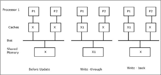
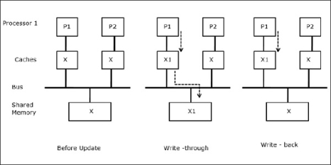
Let X be an element of shared data which has been referenced by two processors, P1 and P2. In the beginning, three copies of X are consistent. If the processor P1 writes a new data X1 into the cache, by using write-through policy, the same copy will be written immediately into the shared memory. In this case, inconsistency occurs between cache memory and the main memory. When a write-back policy is used, the main memory will be updated when the modified data in the cache is replaced or invalidated.
In general, there are three sources of inconsistency problem −
- Sharing of writable data
- Process migration
- I/O activity
Snoopy Bus Protocols
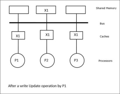
Snoopy protocols achieve data consistency between the cache memory and the shared memory through a bus-based memory system. Write-invalidate and write-update policies are used for maintaining cache consistency.
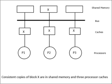
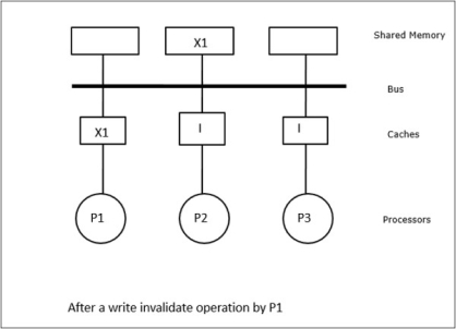
In this case, we have three processors P1, P2, and P3 having a consistent copy of data element ‘X’ in their local cache memory and in the shared memory (Figure-a). Processor P1 writes X1 in its cache memory using write-invalidate protocol. So, all other copies are invalidated via the bus. It is denoted by ‘I’ (Figure-b). Invalidated blocks are also known as dirty, i.e. they should not be used. The write-update protocol updates all the cache copies via the bus. By using write back cache, the memory copy is also updated (Figure-c).
Cache Events and Actions
Following events and actions occur on the execution of memory-access and invalidation commands −
- Read-miss − When a processor wants to read a block and it is not in the cache, a read-miss occurs. This initiates a bus-read operation. If no dirty copy exists, then the main memory that has a consistent copy, supplies a copy to the requesting cache memory. If a dirty copy exists in a remote cache memory, that cache will restrain the main memory and send a copy to the requesting cache memory. In both the cases, the cache copy will enter the valid state after a read miss.
- Write-hit − If the copy is in dirty or reserved state, write is done locally and the new state is dirty. If the new state is valid, write-invalidate command is broadcasted to all the caches, invalidating their copies. When the shared memory is written through, the resulting state is reserved after this first write.
- Write-miss − If a processor fails to write in the local cache memory, the copy must come either from the main memory or from a remote cache memory with a dirty block. This is done by sending a read-invalidate command, which will invalidate all cache copies. Then the local copy is updated with dirty state.
- Read-hit − Read-hit is always performed in local cache memory without causing a transition of state or using the snoopy bus for invalidation.
- Block replacement − When a copy is dirty, it is to be written back to the main memory by block replacement method. However, when the copy is either in valid or reserved or invalid state, no replacement will take place.
Directory-Based Protocols
By using a multistage network for building a large multiprocessor with hundreds of processors, the snoopy cache protocols need to be modified to suit the network capabilities. Broadcasting being very expensive to perform in a multistage network, the consistency commands is sent only to those caches that keep a copy of the block. This is the reason for development of directory-based protocols for network-connected multiprocessors.
In a directory-based protocols system, data to be shared are placed in a common directory that maintains the coherence among the caches. Here, the directory acts as a filter where the processors ask permission to load an entry from the primary memory to its cache memory. If an entry is changed the directory either updates it or invalidates the other caches with that entry.
Hardware Synchronization Mechanisms
Synchronization is a special form of communication where instead of data control, information is exchanged between communicating processes residing in the same or different processors.
Multiprocessor systems use hardware mechanisms to implement low-level synchronization operations. Most multiprocessors have hardware mechanisms to impose atomic operations such as memory read, write or read-modify-write operations to implement some synchronization primitives. Other than atomic memory operations, some inter-processor interrupts are also used for synchronization purposes.
Cache Coherency in Shared Memory Machines
Maintaining cache coherency is a problem in multiprocessor system when the processors contain local cache memory. Data inconsistency between different caches easily occurs in this system.
The major concern areas are −
- Sharing of writable data
- Process migration
- I/O activity
Sharing of writable data
When two processors (P1 and P2) have same data element (X) in their local caches and one process (P1) writes to the data element (X), as the caches are write-through local cache of P1, the main memory is also updated. Now when P2 tries to read data element (X), it does not find X because the data element in the cache of P2 has become outdated.
Process migration
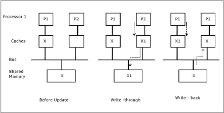
In the first stage, cache of P1 has data element X, whereas P2 does not have anything. A process on P2 first writes on X and then migrates to P1. Now, the process starts reading data element X, but as the processor P1 has outdated data the process cannot read it. So, a process on P1 writes to the data element X and then migrates to P2. After migration, a process on P2 starts reading the data element X but it finds an outdated version of X in the main memory.
I/O activity
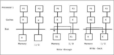
As illustrated in the figure, an I/O device is added to the bus in a two-processor multiprocessor architecture. In the beginning, both the caches contain the data element X. When the I/O device receives a new element X, it stores the new element directly in the main memory. Now, when either P1 or P2 (assume P1) tries to read element X it gets an outdated copy. So, P1 writes to element X. Now, if I/O device tries to transmit X it gets an outdated copy.
Uniform Memory Access (UMA)
Uniform Memory Access (UMA) architecture means the shared memory is the same for all processors in the system. Popular classes of UMA machines, which are commonly used for (file-) servers, are the so-called Symmetric Multiprocessors (SMPs). In an SMP, all system resources like memory, disks, other I/O devices, etc. are accessible by the processors in a uniform manner.
Non-Uniform Memory Access (NUMA)
In NUMA architecture, there are multiple SMP clusters having an internal indirect/shared network, which are connected in scalable message-passing network. So, NUMA architecture is logically shared physically distributed memory architecture.
In a NUMA machine, the cache-controller of a processor determines whether a memory reference is local to the SMP’s memory or it is remote. To reduce the number of remote memory accesses, NUMA architectures usually apply caching processors that can cache the remote data. But when caches are involved, cache coherency needs to be maintained. So these systems are also known as CC-NUMA (Cache Coherent NUMA).
Cache Only Memory Architecture (COMA)
COMA machines are similar to NUMA machines, with the only difference that the main memories of COMA machines act as direct-mapped or set-associative caches. The data blocks are hashed to a location in the DRAM cache according to their addresses. Data that is fetched remotely is actually stored in the local main memory. Moreover, data blocks do not have a fixed home location, they can freely move throughout the system.
COMA architectures mostly have a hierarchical message-passing network. A switch in such a tree contains a directory with data elements as its sub-tree. Since data has no home location, it must be explicitly searched for. This means that a remote access requires a traversal along the switches in the tree to search their directories for the required data. So, if a switch in the network receives multiple requests from its subtree for the same data, it combines them into a single request which is sent to the parent of the switch. When the requested data returns, the switch sends multiple copies of it down its subtree.
COMA versus CC-NUMA
Following are the differences between COMA and CC-NUMA.
- COMA tends to be more flexible than CC-NUMA because COMA transparently supports the migration and replication of data without the need of the OS.
- COMA machines are expensive and complex to build because they need non-standard memory management hardware and the coherency protocol is harder to implement.
- Remote accesses in COMA are often slower than those in CC-NUMA since the tree network needs to be traversed to find the data.
Overview
- Management of I/O devices is a very important part of the operating system - so important and so varied that entire I/O subsystems are devoted to its operation. ( Consider the range of devices on a modern computer, from mice, keyboards, disk drives, display adapters, USB devices, network connections, audio I/O, printers, special devices for the handicapped, and many special-purpose peripherals. )
- I/O Subsystems must contend with two ( conflicting? ) trends: (1) The gravitation towards standard interfaces for a wide range of devices, making it easier to add newly developed devices to existing systems, and (2) the development of entirely new types of devices, for which the existing standard interfaces are not always easy to apply.
- Device drivers are modules that can be plugged into an OS to handle a particular device or category of similar devices.
I/O Hardware
- I/O devices can be roughly categorized as storage, communications, user-interface, and other
- Devices communicate with the computer via signals sent over wires or through the air.
- Devices connect with the computer via ports, e.g. a serial or parallel port.
- A common set of wires connecting multiple devices is termed a bus.
- Buses include rigid protocols for the types of messages that can be sent across the bus and the procedures for resolving contention issues.
- Figure 13.1 below illustrates three of the four bus types commonly found in a modern PC:
- The PCI bus connects high-speed high-bandwidth devices to the memory subsystem ( and the CPU. )
- The expansion bus connects slower low-bandwidth devices, which typically deliver data one character at a time ( with buffering. )
- The SCSI bus connects a number of SCSI devices to a common SCSI controller.
- A daisy-chain bus, ( not shown) is when a string of devices is connected to each other like beads on a chain, and only one of the devices is directly connected to the host.
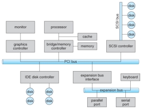
A typical PC bus structure.
- One way of communicating with devices is through registers associated with each port. Registers may be one to four bytes in size, and may typically include ( a subset of ) the following four:
- The data-in register is read by the host to get input from the device.
- The data-out register is written by the host to send output.
- The status register has bits read by the host to ascertain the status of the device, such as idle, ready for input, busy, error, transaction complete, etc.
- The control register has bits written by the host to issue commands or to change settings of the device such as parity checking, word length, or full- versus half-duplex operation.
- Figure shows some of the most common I/O port address ranges.
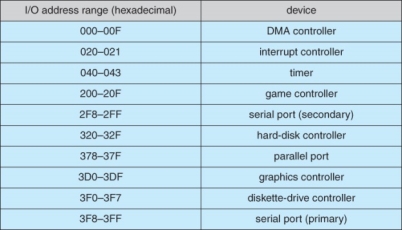
Device I/O port locations on PCs ( partial ).
- Another technique for communicating with devices is memory-mapped I/O.
- In this case a certain portion of the processor's address space is mapped to the device, and communications occur by reading and writing directly to/from those memory areas.
- Memory-mapped I/O is suitable for devices which must move large quantities of data quickly, such as graphics cards.
- Memory-mapped I/O can be used either instead of or more often in combination with traditional registers. For example, graphics cards still use registers for control information such as setting the video mode.
- A potential problem exists with memory-mapped I/O, if a process is allowed to write directly to the address space used by a memory-mapped I/O device.
- ( Note: Memory-mapped I/O is not the same thing as direct memory access, DMA. See section 13.2.3 below. )
Polling
- One simple means of device handshaking involves polling:
- The host repeatedly checks the busy bit on the device until it becomes clear.
- The host writes a byte of data into the data-out register, and sets the write bit in the command register ( in either order. )
- The host sets the command ready bit in the command register to notify the device of the pending command.
- When the device controller sees the command-ready bit set, it first sets the busy bit.
- Then the device controller reads the command register, sees the write bit set, reads the byte of data from the data-out register, and outputs the byte of data.
- The device controller then clears the error bit in the status register, the command-ready bit, and finally clears the busy bit, signaling the completion of the operation.
- Polling can be very fast and efficient, if both the device and the controller are fast and if there is significant data to transfer. It becomes inefficient, however, if the host must wait a long time in the busy loop waiting for the device, or if frequent checks need to be made for data that is infrequently there.
Interrupts
- Interrupts allow devices to notify the CPU when they have data to transfer or when an operation is complete, allowing the CPU to perform other duties when no I/O transfers need its immediate attention.
- The CPU has an interrupt-request line that is sensed after every instruction.
- A device's controller raises an interrupt by asserting a signal on the interrupt request line.
- The CPU then performs a state save, and transfers control to the interrupt handler routine at a fixed address in memory. ( The CPU catches the interrupt and dispatches the interrupt handler. )
- The interrupt handler determines the cause of the interrupt, performs the necessary processing, performs a state restore, and executes a return from interrupt instruction to return control to the CPU. ( The interrupt handler clears the interrupt by servicing the device. )
- ( Note that the state restored does not need to be the same state as the one that was saved when the interrupt went off. See below for an example involving time-slicing. )
- Figure 13.3 illustrates the interrupt-driven I/O procedure:
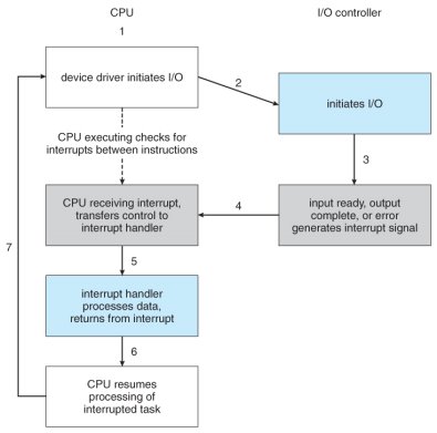
Interrupt-driven I/O cycle.
- The above description is adequate for simple interrupt-driven I/O, but there are three needs in modern computing which complicate the picture:
- The need to defer interrupt handling during critical processing,
- The need to determine which interrupt handler to invoke, without having to poll all devices to see which one needs attention, and
- The need for multi-level interrupts, so the system can differentiate between high- and low-priority interrupts for proper response.
- These issues are handled in modern computer architectures with interrupt-controller hardware.
- Most CPUs now have two interrupt-request lines: One that is non-maskable for critical error conditions and one that is maskable, that the CPU can temporarily ignore during critical processing.
- The interrupt mechanism accepts an address, which is usually one of a small set of numbers for an offset into a table called the interrupt vector. This table ( usually located at physical address zero ? ) holds the addresses of routines prepared to process specific interrupts.
- The number of possible interrupt handlers still exceeds the range of defined interrupt numbers, so multiple handlers can be interrupt chained. Effectively the addresses held in the interrupt vectors are the head pointers for linked-lists of interrupt handlers.
- Figure 13.4 shows the Intel Pentium interrupt vector. Interrupts 0 to 31 are non-maskable and reserved for serious hardware and other errors. Maskable interrupts, including normal device I/O interrupts begin at interrupt 32.
- Modern interrupt hardware also supports interrupt priority levels, allowing systems to mask off only lower-priority interrupts while servicing a high-priority interrupt, or conversely to allow a high-priority signal to interrupt the processing of a low-priority one.
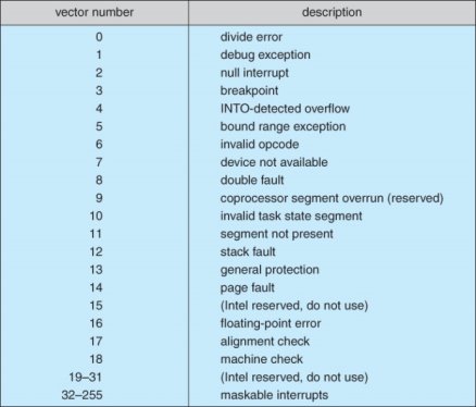
Intel Pentium processor event-vector table.
- At boot time the system determines which devices are present, and loads the appropriate handler addresses into the interrupt table.
- During operation, devices signal errors or the completion of commands via interrupts.
- Exceptions, such as dividing by zero, invalid memory accesses, or attempts to access kernel mode instructions can be signaled via interrupts.
- Time slicing and context switches can also be implemented using the interrupt mechanism.
- The scheduler sets a hardware timer before transferring control over to a user process.
- When the timer raises the interrupt request line, the CPU performs a state-save, and transfers control over to the proper interrupt handler, which in turn runs the scheduler.
- The scheduler does a state-restore of a different process before resetting the timer and issuing the return-from-interrupt instruction.
- A similar example involves the paging system for virtual memory - A page fault causes an interrupt, which in turn issues an I/O request and a context switch as described above, moving the interrupted process into the wait queue and selecting a different process to run. When the I/O request has completed ( i.e. when the requested page has been loaded up into physical memory ), then the device interrupts, and the interrupt handler moves the process from the wait queue into the ready queue, ( or depending on scheduling algorithms and policies, may go ahead and context switch it back onto the CPU. )
- System calls are implemented via software interrupts, a.k.a. Traps. When a ( library ) program needs work performed in kernel mode, it sets command information and possibly data addresses in certain registers, and then raises a software interrupt. ( E.g. 21 hex in DOS. ) The system does a state save and then calls on the proper interrupt handler to process the request in kernel mode. Software interrupts generally have low priority, as they are not as urgent as devices with limited buffering space.
- Interrupts are also used to control kernel operations, and to schedule activities for optimal performance. For example, the completion of a disk read operation involves two interrupts:
- A high-priority interrupt acknowledges the device completion, and issues the next disk request so that the hardware does not sit idle.
- A lower-priority interrupt transfers the data from the kernel memory space to the user space, and then transfers the process from the waiting queue to the ready queue.
- The Solaris OS uses a multi-threaded kernel and priority threads to assign different threads to different interrupt handlers. This allows for the "simultaneous" handling of multiple interrupts, and the assurance that high-priority interrupts will take precedence over low-priority ones and over user processes.
Direct Memory Access
- For devices that transfer large quantities of data ( such as disk controllers ), it is wasteful to tie up the CPU transferring data in and out of registers one byte at a time.
- Instead this work can be off-loaded to a special processor, known as the Direct Memory Access, DMA, Controller.
- The host issues a command to the DMA controller, indicating the location where the data is located, the location where the data is to be transferred to, and the number of bytes of data to transfer. The DMA controller handles the data transfer, and then interrupts the CPU when the transfer is complete.
- A simple DMA controller is a standard component in modern PCs, and many bus-mastering I/O cards contain their own DMA hardware.
- Handshaking between DMA controllers and their devices is accomplished through two wires called the DMA-request and DMA-acknowledge wires.
- While the DMA transfer is going on the CPU does not have access to the PCI bus ( including main memory ), but it does have access to its internal registers and primary and secondary caches.
- DMA can be done in terms of either physical addresses or virtual addresses that are mapped to physical addresses. The latter approach is known as Direct Virtual Memory Access, DVMA, and allows direct data transfer from one memory-mapped device to another without using the main memory chips.
- Direct DMA access by user processes can speed up operations, but is generally forbidden by modern systems for security and protection reasons. ( I.e. DMA is a kernel-mode operation. )
- Figure 13.5 below illustrates the DMA process.
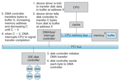
Steps in a DMA transfer.
I/O Hardware Summary
Application I/O Interface
- User application access to a wide variety of different devices is accomplished through layering, and through encapsulating all of the device-specific code into device drivers, while application layers are presented with a common interface for all ( or at least large general categories of ) devices.
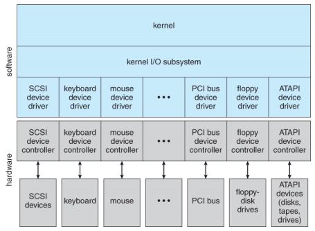
A kernel I/O structure.
- Devices differ on many different dimensions, as outlined in Figure 13.7:
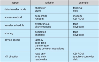
Characteristics of I/O devices.
- Most devices can be characterized as either block I/O, character I/O, memory mapped file access, or network sockets. A few devices are special, such as time-of-day clock and the system timer.
- Most OSes also have an escape, or back door, which allows applications to send commands directly to device drivers if needed. In UNIX this is the ioctl( ) system call ( I/O Control ). Ioctl( ) takes three arguments - The file descriptor for the device driver being accessed, an integer indicating the desired function to be performed, and an address used for communicating or transferring additional information.
Block and Character Devices
- Block devices are accessed a block at a time, and are indicated by a "b" as the first character in a long listing on UNIX systems. Operations supported include read( ), write( ), and seek( ).
- Accessing blocks on a hard drive directly ( without going through the filesystem structure ) is called raw I/O, and can speed up certain operations by bypassing the buffering and locking normally conducted by the OS. ( It then becomes the application's responsibility to manage those issues. )
- A new alternative is direct I/O, which uses the normal filesystem access, but which disables buffering and locking operations.
- Memory-mapped file I/O can be layered on top of block-device drivers.
- Rather than reading in the entire file, it is mapped to a range of memory addresses, and then paged into memory as needed using the virtual memory system.
- Access to the file is then accomplished through normal memory accesses, rather than through read( ) and write( ) system calls. This approach is commonly used for executable program code.
- Character devices are accessed one byte at a time, and are indicated by a "c" in UNIX long listings. Supported operations include get( ) and put( ), with more advanced functionality such as reading an entire line supported by higher-level library routines.
Network Devices
- Because network access is inherently different from local disk access, most systems provide a separate interface for network devices.
- One common and popular interface is the socket interface, which acts like a cable or pipeline connecting two networked entities. Data can be put into the socket at one end, and read out sequentially at the other end. Sockets are normally full-duplex, allowing for bi-directional data transfer.
- The select( ) system call allows servers ( or other applications ) to identify sockets which have data waiting, without having to poll all available sockets.
Clocks and Timers
- Three types of time services are commonly needed in modern systems:
- Get the current time of day.
- Get the elapsed time ( system or wall clock ) since a previous event.
- Set a timer to trigger event X at time T.
- Unfortunately time operations are not standard across all systems.
- A programmable interrupt timer, PIT can be used to trigger operations and to measure elapsed time. It can be set to trigger an interrupt at a specific future time, or to trigger interrupts periodically on a regular basis.
- The scheduler uses a PIT to trigger interrupts for ending time slices.
- The disk system may use a PIT to schedule periodic maintenance cleanup, such as flushing buffers to disk.
- Networks use PIT to abort or repeat operations that are taking too long to complete. I.e. resending packets if an acknowledgement is not received before the timer goes off.
- More timers than actually exist can be simulated by maintaining an ordered list of timer events, and setting the physical timer to go off when the next scheduled event should occur.
- On most systems the system clock is implemented by counting interrupts generated by the PIT. Unfortunately this is limited in its resolution to the interrupt frequency of the PIT, and may be subject to some drift over time. An alternate approach is to provide direct access to a high frequency hardware counter, which provides much higher resolution and accuracy, but which does not support interrupts.
Blocking and Non-blocking I/O
- With blocking I/O a process is moved to the wait queue when an I/O request is made, and moved back to the ready queue when the request completes, allowing other processes to run in the meantime.
- With non-blocking I/O the I/O request returns immediately, whether the requested I/O operation has ( completely ) occurred or not. This allows the process to check for available data without getting hung completely if it is not there.
- One approach for programmers to implement non-blocking I/O is to have a multi-threaded application, in which one thread makes blocking I/O calls ( say to read a keyboard or mouse ), while other threads continue to update the screen or perform other tasks.
- A subtle variation of the non-blocking I/O is the asynchronous I/O, in which the I/O request returns immediately allowing the process to continue on with other tasks, and then the process is notified ( via changing a process variable, or a software interrupt, or a callback function ) when the I/O operation has completed and the data is available for use. ( The regular non-blocking I/O returns immediately with whatever results are available, but does not complete the operation and notify the process later. )
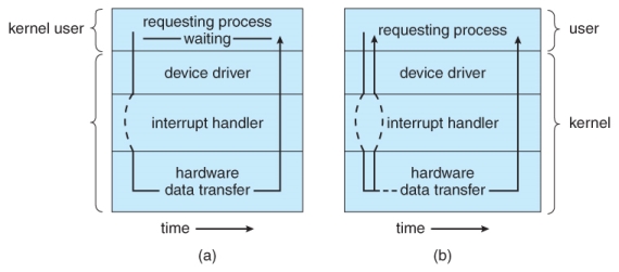
Two I/O methods: (a) synchronous and (b) asynchronous.
Vectored I/O ( NEW )
Kernel I/O Subsystem
I/O Scheduling
- Scheduling I/O requests can greatly improve overall efficiency. Priorities can also play a part in request scheduling.
- The classic example is the scheduling of disk accesses, as discussed in detail in chapter 12.
- Buffering and caching can also help, and can allow for more flexible scheduling options.
- On systems with many devices, separate request queues are often kept for each device:
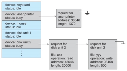
Device-status table.
Buffering
- Buffering of I/O is performed for ( at least ) 3 major reasons:
- Speed differences between two devices. ( See Figure 13.10 below. ) A slow device may write data into a buffer, and when the buffer is full, the entire buffer is sent to the fast device all at once. So that the slow device still has somewhere to write while this is going on, a second buffer is used, and the two buffers alternate as each becomes full. This is known as double buffering. ( Double buffering is often used in ( animated ) graphics, so that one screen image can be generated in a buffer while the other ( completed ) buffer is displayed on the screen. This prevents the user from ever seeing any half-finished screen images. )
- Data transfer size differences. Buffers are used in particular in networking systems to break messages up into smaller packets for transfer, and then for re-assembly at the receiving side.
- To support copy semantics. For example, when an application makes a request for a disk write, the data is copied from the user's memory area into a kernel buffer. Now the application can change their copy of the data, but the data which eventually gets written out to disk is the version of the data at the time the write request was made.
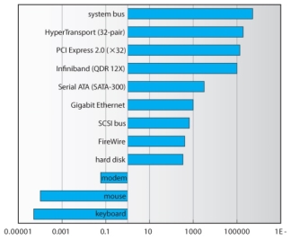
Sun Enterprise 6000 device-transfer rates ( logarithmic ).
Caching
- Caching involves keeping a copy of data in a faster-access location than where the data is normally stored.
- Buffering and caching are very similar, except that a buffer may hold the only copy of a given data item, whereas a cache is just a duplicate copy of some other data stored elsewhere.
- Buffering and caching go hand-in-hand, and often the same storage space may be used for both purposes. For example, after a buffer is written to disk, then the copy in memory can be used as a cached copy, (until that buffer is needed for other purposes. )
Spooling and Device Reservation
- A spool ( Simultaneous Peripheral Operations On-Line ) buffers data for ( peripheral ) devices such as printers that cannot support interleaved data streams.
- If multiple processes want to print at the same time, they each send their print data to files stored in the spool directory. When each file is closed, then the application sees that print job as complete, and the print scheduler sends each file to the appropriate printer one at a time.
- Support is provided for viewing the spool queues, removing jobs from the queues, moving jobs from one queue to another queue, and in some cases changing the priorities of jobs in the queues.
- Spool queues can be general ( any laser printer ) or specific ( printer number 42. )
- OSes can also provide support for processes to request / get exclusive access to a particular device, and/or to wait until a device becomes available.
Error Handling
- I/O requests can fail for many reasons, either transient ( buffers overflow ) or permanent ( disk crash ).
- I/O requests usually return an error bit ( or more ) indicating the problem. UNIX systems also set the global variable errno to one of a hundred or so well-defined values to indicate the specific error that has occurred. ( See errno.h for a complete listing, or man errno. )
- Some devices, such as SCSI devices, are capable of providing much more detailed information about errors, and even keep an on-board error log that can be requested by the host.
I/O Protection
- The I/O system must protect against either accidental or deliberate erroneous I/O.
- User applications are not allowed to perform I/O in user mode - All I/O requests are handled through system calls that must be performed in kernel mode.
- Memory mapped areas and I/O ports must be protected by the memory management system, but access to these areas cannot be totally denied to user programs. ( Video games and some other applications need to be able to write directly to video memory for optimal performance for example. ) Instead the memory protection system restricts access so that only one process at a time can access particular parts of memory, such as the portion of the screen memory corresponding to a particular window.
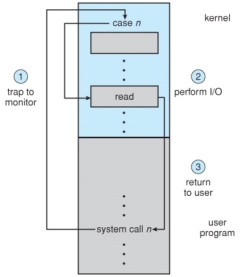
Use of a system call to perform I/O.
Kernel Data Structures
- The kernel maintains a number of important data structures pertaining to the I/O system, such as the open file table.
- These structures are object-oriented, and flexible to allow access to a wide variety of I/O devices through a common interface. ( See Figure 13.12 below. )
- Windows NT carries the object-orientation one step further, implementing I/O as a message-passing system from the source through various intermediaries to the device.
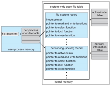
UNIX I/O kernel structure.
Kernel I/O Subsystem Summary
Transforming I/O Requests to Hardware Operations
- Users request data using file names, which must ultimately be mapped to specific blocks of data from a specific device managed by a specific device driver.
- DOS uses the colon separator to specify a particular device ( e.g. C:, LPT:, etc. )
- UNIX uses a mount table to map filename prefixes ( e.g. /usr ) to specific mounted devices. Where multiple entries in the mount table match different prefixes of the filename the one that matches the longest prefix is chosen. ( e.g. /usr/home instead of /usr where both exist in the mount table and both match the desired file. )
- UNIX uses special device files, usually located in /dev, to represent and access physical devices directly.
- Each device file has a major and minor number associated with it, stored and displayed where the file size would normally go.
- The major number is an index into a table of device drivers, and indicates which device driver handles this device. ( E.g. The disk drive handler. )
- The minor number is a parameter passed to the device driver, and indicates which specific device is to be accessed, out of the many which may be handled by a particular device driver. ( e.g. a particular disk drive or partition. )
- A series of lookup tables and mappings makes the access of different devices flexible, and somewhat transparent to users.
- Figure 13.13 illustrates the steps taken to process a ( blocking ) read request:
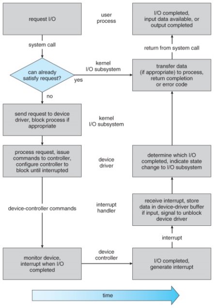
The life cycle of an I/O request.
STREAMS ( Optional )
- The streams mechanism in UNIX provides a bi-directional pipeline between a user process and a device driver, onto which additional modules can be added.
- The user process interacts with the stream head.
- The device driver interacts with the device end.
- Zero or more stream modules can be pushed onto the stream, using ioctl( ). These modules may filter and/or modify the data as it passes through the stream.
- Each module has a read queue and a write queue.
- Flow control can be optionally supported, in which case each module will buffer data until the adjacent module is ready to receive it. Without flow control, data is passed along as soon as it is ready.
- User processes communicate with the stream head using either read( ) and write( ) ( or putmsg( ) and getmsg( ) for message passing. )
- Streams I/O is asynchronous ( non-blocking ), except for the interface between the user process and the stream head.
- The device driver must respond to interrupts from its device - If the adjacent module is not prepared to accept data and the device driver's buffers are all full, then data is typically dropped.
- Streams are widely used in UNIX, and are the preferred approach for device drivers. For example, UNIX implements sockets using streams.
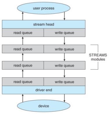
The SREAMS structure.
Performance ( Optional )
- The I/O system is a major factor in overall system performance, and can place heavy loads on other major components of the system ( interrupt handling, process switching, memory access, bus contention, and CPU load for device drivers just to name a few. )
- Interrupt handling can be relatively expensive ( slow ), which causes programmed I/O to be faster than interrupt-driven I/O when the time spent busy waiting is not excessive.
- Network traffic can also put a heavy load on the system. Consider for example the sequence of events that occur when a single character is typed in a telnet session, as shown in figure 13.15. ( And the fact that a similar set of events must happen in reverse to echo back the character that was typed. ) Sun uses in-kernel threads for the telnet daemon, increasing the supportable number of simultaneous telnet sessions from the hundreds to the thousands.
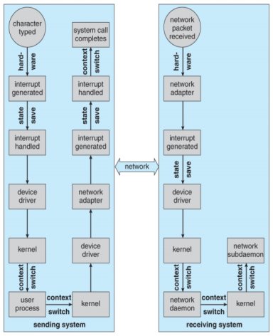
Figure - Intercomputer communications.
- Other systems use front-end processors to off-load some of the work of I/O processing from the CPU. For example a terminal concentrator can multiplex with hundreds of terminals on a single port on a large computer.
- Several principles can be employed to increase the overall efficiency of I/O processing:
- Reduce the number of context switches.
- Reduce the number of times data must be copied.
- Reduce interrupt frequency, using large transfers, buffering, and polling where appropriate.
- Increase concurrency using DMA.
- Move processing primitives into hardware, allowing their operation to be concurrent with CPU and bus operations.
- Balance CPU, memory, bus, and I/O operations, so a bottleneck in one does not idle all the others.
- The development of new I/O algorithms often follows a progression from application level code to on-board hardware implementation, as shown in Figure 13.16. Lower-level implementations are faster and more efficient, but higher-level ones are more flexible and easier to modify. Hardware-level functionality may also be harder for higher-level authorities ( e.g. The kernel ) to control.
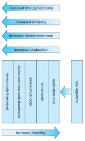
Device functionality progression.
The method that is used to transfer information between internal storage and external I/O devices is known as I/O interface. The CPU is interfaced using special communication links by the peripherals connected to any computer system. These communication links are used to resolve the differences between CPU and peripheral. There exists special hardware components between CPU and peripherals to supervise and synchronize all the input and output transfers that are called interface units.
Mode of Transfer:
The binary information that is received from an external device is usually stored in the memory unit. The information that is transferred from the CPU to the external device is originated from the memory unit. CPU merely processes the information but the source and target is always the memory unit. Data transfer between CPU and the I/O devices may be done in different modes.
Data transfer to and from the peripherals may be done in any of the three possible ways
- Programmed I/O.
- Interrupt- initiated I/O.
- Direct memory access( DMA).
Now let’s discuss each mode one by one.
- Programmed I/O: It is due to the result of the I/O instructions that are written in the computer program. Each data item transfer is initiated by an instruction in the program. Usually the transfer is from a CPU register and memory. In this case it requires constant monitoring by the CPU of the peripheral devices.
Example of Programmed I/O: In this case, the I/O device does not have direct access to the memory unit. A transfer from I/O device to memory requires the execution of several instructions by the CPU, including an input instruction to transfer the data from device to the CPU and store instruction to transfer the data from CPU to memory. In programmed I/O, the CPU stays in the program loop until the I/O unit indicates that it is ready for data transfer. This is a time consuming process since it needlessly keeps the CPU busy. This situation can be avoided by using an interrupt facility. This is discussed below.
2. Interrupt- initiated I/O: Since in the above case we saw the CPU is kept busy unnecessarily. This situation can very well be avoided by using an interrupt driven method for data transfer. By using interrupt facility and special commands to inform the interface to issue an interrupt request signal whenever data is available from any device. In the meantime the CPU can proceed for any other program execution. The interface meanwhile keeps monitoring the device. Whenever it is determined that the device is ready for data transfer it initiates an interrupt request signal to the computer. Upon detection of an external interrupt signal the CPU stops momentarily the task that it was already performing, branches to the service program to process the I/O transfer, and then return to the task it was originally performing.
Note: Both the methods programmed I/O and Interrupt-driven I/O require the active intervention of the
processor to transfer data between memory and the I/O module, and any data transfer must transverse
a path through the processor. Thus both these forms of I/O suffer from two inherent drawbacks.
- The I/O transfer rate is limited by the speed with which the processor can test and service a
device. - The processor is tied up in managing an I/O transfer; a number of instructions must be executed
for each I/O transfer.
- Direct Memory Access: The data transfer between a fast storage media such as magnetic disk and memory unit is limited by the speed of the CPU. Thus we can allow the peripherals directly communicate with each other using the memory buses, removing the intervention of the CPU. This type of data transfer technique is known as DMA or direct memory access. During DMA the CPU is idle and it has no control over the memory buses. The DMA controller takes over the buses to manage the transfer directly between the I/O devices and the memory unit.
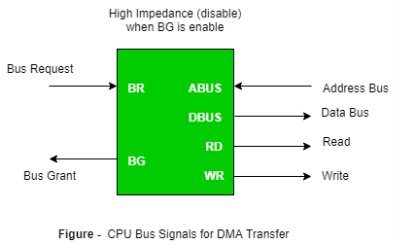
Bus Request : It is used by the DMA controller to request the CPU to relinquish the control of the buses.
Bus Grant : It is activated by the CPU to Inform the external DMA controller that the buses are in high impedance state and the requesting DMA can take control of the buses. Once the DMA has taken the control of the buses it transfers the data. This transfer can take place in many ways.
Types of DMA transfer using DMA controller:
Burst Transfer :
DMA returns the bus after complete data transfer. A register is used as a byte count,
being decremented for each byte transfer, and upon the byte count reaching zero, the DMAC will
release the bus. When the DMAC operates in burst mode, the CPU is halted for the duration of the data
transfer.
Steps involved are:
- Bus grant request time.
- Transfer the entire block of data at transfer rate of device because the device is usually slow than the
speed at which the data can be transferred to CPU. - Release the control of the bus back to CPU
So, total time taken to transfer the N bytes
= Bus grant request time + (N) * (memory transfer rate) + Bus release control time.
Where,
X µsec =data transfer time or preparation time (words/block)
Y µsec =memory cycle time or cycle time or transfer time (words/block)
% CPU idle (Blocked)=(Y/X+Y)*100
% CPU Busy=(X/X+Y)*100
Cyclic Stealing :
An alternative method in which DMA controller transfers one word at a time after which it must return the control of the buses to the CPU. The CPU delays its operation only for one memory cycle to allow the direct memory I/O transfer to “steal” one memory cycle.
Steps Involved are:
- Buffer the byte into the buffer
- Inform the CPU that the device has 1 byte to transfer (i.e. bus grant request)
- Transfer the byte (at system bus speed)
- Release the control of the bus back to CPU.
Before moving on transfer next byte of data, device performs step 1 again so that bus isn’t tied up and
the transfer won’t depend upon the transfer rate of device.
So, for 1 byte of transfer of data, time taken by using cycle stealing mode (T).
= time required for bus grant + 1 bus cycle to transfer data + time required to release the bus, it will be
N x T
In cycle stealing mode we always follow pipelining concept that when one byte is getting transferred then Device is parallel preparing the next byte. “The fraction of CPU time to the data transfer time” if asked then cycle stealing mode is used.
Where,
X µsec =data transfer time or preparation time
(words/block)
Y µsec =memory cycle time or cycle time or transfer
Time (words/block)
% CPU idle (Blocked) =(Y/X)*100
% CPU busy=(X/Y)*100
Interleaved mode: In this technique , the DMA controller takes over the system bus when the
microprocessor is not using it.An alternate half cycle i.e. half cycle DMA + half cycle processor.
Data transfer between the CPU and I/O devices can be done in variety of modes. These are three possible modes:
- Programmed I/O
- Interrupt initiated I/O
- Direct Memory Access (DMA)
In this article we shall discuss the first two modes only.
1. Programmed I/O :
In this mode the data transfer is initiated by the instructions written in a computer program. An input instruction is required to store the data from the device to the CPU and a store instruction is required to transfer the data from the CPU to the device. Data transfer through this mode requires constant monitoring of the peripheral device by the CPU and also monitor the possibility of new transfer once the transfer has been initiated. Thus CPU stays in a loop until the I/O device indicates that it is ready for data transfer. Thus programmed I/O is a time consuming process that keeps the processor busy needlessly and leads to wastage of the CPU cycles.
This can be overcome by the use of an interrupt facility. This forms the basis for the Interrupt Initiated I/O.
2. Interrupt Initiated I/O :
This mode uses an interrupt facility and special commands to inform the interface to issue the interrupt command when data becomes available and interface is ready for the data transfer. In the meantime CPU keeps on executing other tasks and need not check for the flag. When the flag is set, the interface is informed and an interrupt is initiated. This interrupt causes the CPU to deviate from what it is doing to respond to the I/O transfer. The CPU responds to the signal by storing the return address from the program counter (PC) into the memory stack and then branches to service that processes the I/O request. After the transfer is complete, CPU returns to the previous task it was executing. The branch address of the service can be chosen in two ways known as vectored and non-vectored interrupt. In vectored interrupt, the source that interrupts, supplies the branch information to the CPU while in case of non-vectored interrupt the branch address is assigned to a fixed location in memory.
Difference between Programmed and Interrupt Initiated I/O :
Programmed I/O | Interrupt Initiated I/O |
Data transfer is initiated by the means of instructions stored in the computer program. Whenever there is a request for I/O transfer the instructions are executed from the program. | The I/O transfer is initiated by the interrupt command issued to the CPU. |
The CPU stays in the loop to know if the device is ready for transfer and has to continuously monitor the peripheral device. | There is no need for the CPU to stay in the loop as the interrupt command interrupts the CPU when the device is ready for data transfer. |
This leads to the wastage of CPU cycles as CPU remains busy needlessly and thus the efficiency of system gets reduced. | The CPU cycles are not wasted as CPU and hence this method is more efficient. |
CPU cannot do any work until the transfer is complete as it has to stay in the loop to continuously monitor the peripheral device. | CPU can do any other work until it is interrupted by the command indicating the readiness of device for data transfer |
Its module is treated as a slow module. | Its module is faster than programmed I/O module. |
It is quite easy to program and understand. | It can be tricky and complicated to understand if one uses low level language. |
The performance of the system is severely degraded. | The performance of the system is enhanced to some extent. |
References:
1. “Digital Design”, M Morris Mano, Prentice Hall, Third Edition
2. “Computer organization” , Hamacher and Zaky, Fifth Edition
3. “Computer Organization and Design: The Hardware Software Interface” D. Patterson, J. Hennessy, Fourth Edition, Morgan Kaufmann
4. “ Microprocessors and interfacing-programming and hardware” Douglas V. Hall and SSSP Rao, McGraw-Hill ,Third Edition
