UNIT 6
Bipolar Junction Transistors
The three types of configurations are Common Base, Common Emitter and Common Collector configurations. In every configuration, the emitter junction is forward biased and the collector junction is reverse biased.
Common Base CB
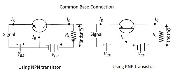
The name itself implies that the Base terminal is taken as common terminal for both input and output of the transistor. The common base connection for both NPN and PNP transistors is as shown in the following figure.

For the sake of understanding, let us consider NPN transistor in CB configuration. When the emitter voltage is applied, as it is forward biased, the electrons from the negative terminal repel the emitter electrons and current flows through the emitter and base to the collector to contribute collector current. The collector voltage VCB is kept constant throughout this.
In the CB configuration, the input current is the emitter current IE and the output current is the collector current IC.
Current Amplification Factor α
The ratio of change in collector current ΔIC to the change in emitter current ΔIE when collector voltage VCB is kept constant, is called as Current amplification factor. It is denoted by α.
α=ΔIC/ΔIE atconstantVCB
Expression for Collector current
Along with the emitter current flowing, there is some amount of base current IB which flows through the base terminal due to electron hole recombination. As collector-base junction is reverse biased, there is another current which is flown due to minority charge carriers. This is the leakage current which can be understood as Ileakage. This is due to minority charge carriers and hence very small.
The emitter current that reaches the collector terminal is
αIE
Total collector current
IC=αIE+Ileakage
If the emitter-base voltage VEB = 0, even then, there flows a small leakage current, which can be termed as ICBO collector−basecurrentwithoutputopencollector−basecurrentwithoutputopen.
The collector current therefore can be expressed as
IC=αIE+ICBO
IE=IC+IB
IC=α(IC+IB)+ICBO
IC(1−α)=αIB+ICBO
IC=(α1−α)IB+(ICBO1−α)
IC=(α1−α)IB+(11−α)ICBO
Hence the above derived is the expression for collector current. The value of collector current depends on base current and leakage current along with the current amplification factor of that transistor in use.
Characteristics of CB configuration
- This configuration provides voltage gain but no current gain.
- Being VCB constant, with a small increase in the Emitter-base voltage VEB, Emitter current IE gets increased.
- Emitter Current IE is independent of Collector voltage VCB.
- Collector Voltage VCB can affect the collector current IC only at low voltages, when VEB is kept constant.
- The input resistance ri is the ratio of change in emitter-base voltage ΔVEB to the change in emitter current ΔIE$ at constant collector base voltage VCB.
η=ΔVEB/ΔIE atconstantVCB
- As the input resistance is of very low value, a small value of VEB is enough to produce a large current flow of emitter current IE.
- The output resistance ro is the ratio of change in the collector base voltage $ΔVCB$$ΔVCB$ to the change in collector current ΔIC at constant emitter current IE.
Ro=ΔVCB/ΔIC atconstantlE
- As the output resistance is of very high value, a large change in VCB produces a very little change in collector current IC.
- This Configuration provides good stability against increase in temperature.
- The CB configuration is used for high frequency applications.
Common Emitter CE
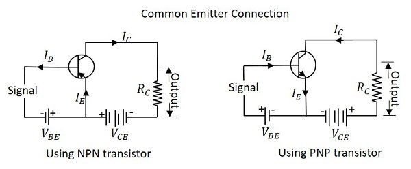
The name itself implies that the Emitter terminal is taken as common terminal for both input and output of the transistor. The common emitter connection for both NPN and PNP transistors is as shown in the following figure.
Just as in CB configuration, the emitter junction is forward biased and the collector junction is reverse biased. The flow of electrons is controlled in the same manner. The input current is the base current IB and the output current is the collector current IC here.
Base Current Amplification factor β
The ratio of change in collector current ΔIC to the change in base current ΔIB is known as Base Current Amplification Factor. It is denoted by β
β=ΔICΔ/IB
Relation between β and α
Let us try to derive the relation between base current amplification factor and emitter current amplification factor.
β=ΔIC/ΔIB
α=ΔIC/ΔIE
IE=IB+IC
ΔIE=ΔIB+ΔIC
ΔIB=ΔIE−ΔIC
We can write
β=ΔIC/ΔIE−ΔIC
Dividing by ΔIE
β=ΔIC/ΔIE/ΔIE/ΔIE−ΔIC/ΔIE
We have
α=ΔIC/ΔIE
Therefore,
β=α/1−α
From the above equation, it is evident that, as α approaches 1, β reaches infinity.
Hence, the current gain in Common Emitter connection is very high. This is the reason this circuit connection is mostly used in all transistor applications.
Expression for Collector Current
In the Common Emitter configuration, IB is the input current and IC is the output current.
We know
IE=IB+IC
And
IC=αIE+ICBO
=α(IB+IC)+ICBO
IC(1−α)=αIB+ICBO
IC=α/1−α IB+1/1−α ICBO
If base circuit is open, i.e. if IB = 0,
The collector emitter current with base open is ICEO
ICEO=1/1−αICBO
Substituting the value of this in the previous equation, we get
IC=α/1−α . IB+ ICEO
IC=βIB+ICEO
Hence the equation for collector current is obtained.
Knee Voltage
In CE configuration, by keeping the base current IB constant, if VCE is varied, IC increases nearly to 1v of VCE and stays constant thereafter. This value of VCE up to which collector current IC changes with VCE is called the Knee Voltage. The transistors while operating in CE configuration, they are operated above this knee voltage.
Characteristics of CE Configuration
- This configuration provides good current gain and voltage gain.
- Keeping VCE constant, with a small increase in VBE the base current IB increases rapidly than in CB configurations.
- For any value of VCE above knee voltage, IC is approximately equal to βIB.
- The input resistance ri is the ratio of change in base emitter voltage ΔVBE to the change in base current ΔIB at constant collector emitter voltage VCE.
Ri=ΔVBE/ΔIB at constant VCE
- As the input resistance is of very low value, a small value of VBE is enough to produce a large current flow of base current IB.
- The output resistance ro is the ratio of change in collector emitter voltage ΔVCE to the change in collector current ΔIC at constant IB.
Ro=ΔVCE/ΔIC at constant IB
- As the output resistance of CE circuit is less than that of CB circuit.
- This configuration is usually used for bias stabilization methods and audio frequency applications.
Common Collector CC Configuration
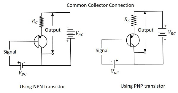
The name itself implies that the Collector terminal is taken as common terminal for both input and output of the transistor. The common collector connection for both NPN and PNP transistors is as shown in the following figure.
Just as in CB and CE configurations, the emitter junction is forward biased and the collector junction is reverse biased. The flow of electrons is controlled in the same manner. The input current is the base current IB and the output current is the emitter current IE here.
Current Amplification Factor γ
The ratio of change in emitter current ΔIE to the change in base current ΔIB is known as Current Amplification factor in common collector CC configuration. It is denoted by γ.
γ=ΔIE/ΔIB
- The current gain in CC configuration is same as in CE configuration.
- The voltage gain in CC configuration is always less than 1.
Relation between γ and α
Let us try to draw some relation between γ and α
γ=ΔIE/ΔIB
α=ΔIC/ΔIE
IE=IB+IC
ΔIE=ΔIB+ΔIC
ΔIB=ΔIE−ΔIC
Substituting the value of IB, we get
γ=ΔIE/ΔIE−ΔIC
Dividing by ΔIEΔIE
γ=ΔIE/ΔIE/ΔIE/ΔIE−ΔIC/ΔIE
1/1−α1
γ=1/1−α
Expression for collector current
We know
IC=αIE+ICBOIC=αIE+ICBO
IE=IB+IC=IB+(αIE+ICBO)IE=IB+IC=IB+(αIE+ICBO)
IE(1−α)=IB+ICBOIE(1−α)=IB+ICBO
IE=IB1−α+ICBO1−αIE=IB1−α+ICBO1−α
IC≅IE=(β+1)IB+(β+1)ICBO
The above is the expression for collector current.
Characteristics of CC Configuration
- This configuration provides current gain but no voltage gain.
- In CC configuration, the input resistance is high and the output resistance is low.
- The voltage gain provided by this circuit is less than 1.
- The sum of collector current and base current equals emitter current.
- The input and output signals are in phase.
- This configuration works as non-inverting amplifier output.
- This circuit is mostly used for impedance matching. That means, to drive a low impedance load from a high impedance source.
- Voltage Divider Bias
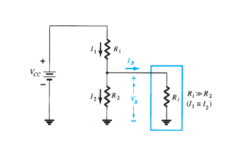
Approximate analysis
VB = R2 Vcc/ R1 + R2
IE = V E / RE
Ri = (β + 1) RE ͌ β RE
β RE ≥ 10 R2
ICQ = IE
VE = VB – VBE
VCEQ = Vcc – Ic(RC + RE)
Transistor Analysis
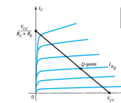
IC sat = IC max = Vcc/ Rc + RE
Load Line Analysis
Ic = Vcc/ Rc + RE | Vce =0V
VCE = VCC| Ic =0mA
Determine the levels of ICQ and VCEQ for voltage divider configuration using exact and approximate techniques and compare solutions.
β . RE ≥ 10 R2
(50)(1.2 k Ω) ≥ 10(22 k Ω)
 60kΩ≥ 220kΩ
Rth = R1 || R2 82 kΩ || 22 kΩ = 17.35 kΩ
Eth = R2 Vcc/ R1 + R2 = 22kΩ (18V)/ 82kΩ + 22kΩ = 3.81 V
IB = Eth – VBE/ Rth + (β +1) RE = 3.81 V – 0.7V / 17.35 kΩ + (51 )(1.2kΩ) = 3.11/ 78.55 kΩ = 39.6 μ A
ICQ = β IB = (50)(39.6μA) = 1.98 mA
VCEQ = Vcc – IC(RC + RE)
= 18V – (1.98mA)(5.6kΩ + 1.2 kΩ)= 4.54V
BJT Amplifier
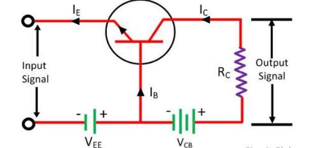
Transistor raises the strength of a weak signal and hence acts an amplifier. The transistor amplifier circuit is shown in the figure below.
Transistor as an Amplifier
The transistor has three terminals namely emitter, base and collector. The emitter and base of the transistor are connected in forward biased and the collector base region is in reverse bias. The forward bias means the P-region of the transistor is connected to the positive terminal of the supply and the negative region is connected to the N-terminal and in reverse bias just opposite of it has occurred.
Vee is applied to the input circuit along with the input signal to achieve the amplification. The DC voltage VEE keeps the emitter-base junction under the forward biased condition regardless of the polarity of the input signal and is known as bias voltage.
When a weak signal is applied to the input, a small change in signal voltage causes a change in emitter current this change is almost the same in collector current because of the transmitter action.
In the collector circuit, a load resistor RC of high value is connected. When collector current flows through such a high resistance, it produces a large voltage drop across it. Thus, a weak signal (0.1V) applied to the input circuit appears in the amplified form (10V) in the collector circuit.
Input Resistance
When the input circuit is forward biased, the input resistance will be low. The input resistance is the opposition offered by the base-emitter junction to the signal flow.
Hence, it is the ratio of small change in base-emitter voltage (ΔVBE) to the resulting change in base current (ΔIB) at constant collector-emitter voltage.
Input resistance, Ri=ΔVBE/ΔIb
Where Ri = input resistance, VBE = base-emitter voltage, and IB = base current.
Output Resistance
The output resistance of a transistor amplifier is very high. The collector current changes very slightly with the change in collector-emitter voltage.
The ratio of change in collector-emitter voltage (ΔVCE) to the resulting change in collector current (ΔIC) at constant base current.
Output resistance = Ro=ΔVCE/ΔIC
Where Ro = Output resistance, VCE = Collector-emitter voltage, and IC = Collector-emitter voltage.
Current gain
It is the ratio of change in collector current (ΔIC) to the change in base current (ΔIB).
Current gain, β=ΔIC/ ΔIB
Voltage Gain
It is the ratio of change in output voltage (ΔVCE) to the change in input voltage (ΔVBE).
Voltage gain, AV=ΔVCE/ΔVBE
= ΔIC x RAC / ΔIB x Ri = ΔIC / ΔIB x RAC / Ri = β x R AC/ Ri
Power Gain
It is the ratio of output signal power to the input signal power.
Power gain Ap = (ΔIC) 2 x RAC / (ΔIB ) 2 x Ri
= (ΔIC / ΔIB) x ΔIC x RAC / ΔIB x Ri
= current gain x voltage gain
BJT as a Switch
For switching applications transistor is biased to operate in the saturation or cutoff region. Transistor in cutoff region will act as an open switching whereas in saturation will act as a closed switch.
Open Switch
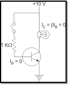
In the cutoff region (both junctions are reversed biased) the voltage across the CE junction is very high. The input voltage is zero so both base and collector currents are zero, hence the resistance offered by the BJT us very high (ideally infinite).
Closed Switch
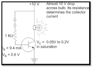
In saturation (both junctions are forward biased) a high input voltage is applied to the base. The value of base resistance is adjusted such that a large base current flows. There is a small voltage drop across the collector emitter junction of the order of 0.05 to 0.2 V and collector current is very large. A very small voltage drop takes place across the BJT and it can be said to be equivalent to a closed switch.
BJT as Amplifier
Single Stage RC Coupled CE Amplifier
The figure shows a single stage CE amplifier. C1 and C3 are coupling capacitors, they are used for blocking the DC component and passing only ac part they also ensure that the DC basing conditions of the BJT remains unchanged even after input is applied. C2 is the bypass capacitor which increases the voltage gain and bypasses the R4 resistor for AC signals.
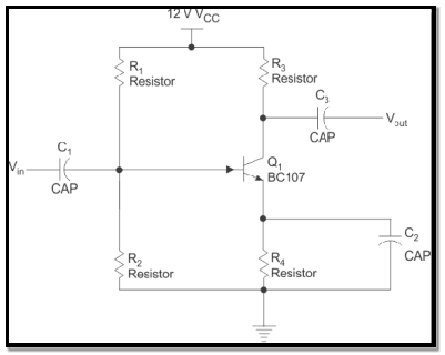
The BJT is biased in the active region using the necessary biasing components. The Q point is made stable in the active region of the transistor. When input is applied as shown below the base current starts to vary up and down, hence collector current also varies as IC = β × IB. Therefore voltage across R3 varies as the collector current is passing through it. Voltage across R3 is the amplified one and is 180o apart from the input signal. Thus voltage across R3 is coupled to the load and amplification has taken place. If the Q point is maintained to be at the center of the load very less or no waveform distortion will take place. The voltage as well as current gain of the CE amplifier is high (gain is the factor by which the voltage of current increases from input to output). It is commonly used in radios and as low frequency voltage amplifier.
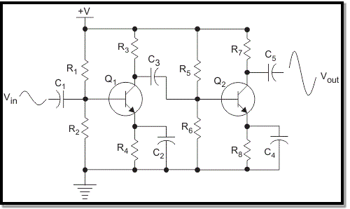
To further increase the gain multistage amplifiers are used. They are connected via capacitor, electrical transformer, R-L or directly coupled depending on the application. The overall gain is the product of gains of individual stages. Figure below shows a two stage CE amplifier.
References:
1. Electrical Technology (Volume I & 2), B L Thereja, 22nd edition, S Chand & Company Ltd
2. Basic Electrical Engineering, V K Mehta, Revised edition, S Chand & Company Ltd
3. Basic Electronics Solid State, B L Thereja, Revised edition, S Chand & Company Ltd
4. Digital Principles and Applications, Albert Malvino , Donald Leach, Tata McGraw Hills Publication
5. Principles of Electronic Devices and Circuits (Analog and Digital), B. L. Theraja , R. S. Sedha , S. Chand publication