UNIT-1
SEMICONDUCTOR PHYSICS
1.1.1 CLASSIFICATION OF SOLIDS
The Band Model
Bands are formed by the closely spaced orbitals.
There are three types of bands:
1. Valance Bands: A valence band is a group of orbitals that contain electrons in the shell. Or we can say It is also defined as the energy band that comprises of valence electrons present in the outermost shell of an atomic structure.
These valence electrons, when provided with sufficient energy, get changed into free electrons and moves to the conduction band thereby causing conductivity. It is at a lower energy level than the conduction band in the energy level diagram.
2. Conduction Band: A conduction band is a group of empty orbitals of the shells that do not contain any electron due to their configuration making the orbitals of higher energy levels.
When the electrons pass from the valance band to the conduction band these solids conduct electricity with the flow of charges in the form of electrons.
3. Forbidden Energy Band: These two bands are separated by a certain amount of energy known as the forbidden energy gap. In this band not a single electron is available. Its diagram is named Band Gap.
Let us distinguish between conductors, semiconductors, and insulators based on these bands.
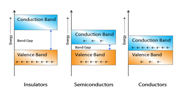
Figure 1: Conductors, Semiconductors, and Insulators based on these bands.
- In Conductors: The valance band and the conduction band overlap each other. This makes it easy for electricity to pass through them. In conductors, the valence band is either not fully occupied with electrons, or the filled valence band overlaps with the empty conduction band. In general, both states occur at the same time, the electrons can therefore move inside the partially filled valence band or inside the two overlapping bands. In conductors, there is no bandgap between the valence band and conduction band.
- In Semi-conductors: there is a slight gap between the conduction band and the valance band. This bandgap is less than or equal to 1.4 eV. The electrons from the valance shell take a little energy to excite from the valance band to the conduction band. Even in semiconductors, there is a bandgap, but compared to insulators it is so small that even at room temperature electrons from the valence band can be lifted into the conduction band. The electrons can move freely and act as charge carriers.
- In Insulators: In insulators, the valence band is fully occupied with electrons due to the covalent bonds. To achieve conductivity, electrons from the valence band have to move into the conduction band. the energy gap is considerably large and the electrons of the valance band cannot be excited to the conduction band before the melting or the dissociation of the solid. This means that under the practically ambient condition it cannot conduct electricity.
Consider an isolated silicon atom; its energy levels are quantized. When two identical atoms are brought closer together, the quantized energy levels hybridize and split into two different levels because of the mutual interaction of the two atoms. More generally, when N atoms are moved closer until they reach the equilibrium inter-atomic distance d, the energy levels split into N levels. These N levels are very close to each other if N is large (which is the case in a crystal) so that they eventually form a continuous energy band.

Figure 2: Formation of Energy band as a function of interatomic distance (distance between atoms)
Key Takeaways
- Semiconductors are materials that have conductivity between conductors and insulators.
- Bands are formed by the closely spaced orbitals.
- There are three types of bands: Valence band, conduction band, Forbidden Energy Band
- On the basis of band theory we can classify the materials as conductors, semiconductors, and insulators based on these bands.
1.1.2 FERMI LEVEL (DEFINITION)
Fermi level" is the term used to describe the top of the collection of electron energy levels at absolute zero temperature. This concept comes from Fermi-Dirac statistics. Electrons are fermions and by the Pauli exclusion principle cannot exist in identical energy states. So at absolute zero they pack into the lowest available energy states and build up a "Fermi sea" of electron energy states. The Fermi level is the surface of that sea at absolute zero where no electrons will have enough energy to rise above the surface.
The concept of the Fermi energy is a crucially important concept for the understanding of the electrical and thermal properties of solids. Both ordinary electrical and thermal processes involve energies of a small fraction of an electron volt. But the Fermi energies of metals are on the order of electron volts. This implies that the vast majority of the electrons cannot receive energy from those processes because there are no available energy states for them to go to within a fraction of an electron volt of their present energy. Limited to a tiny depth of energy, these interactions are limited to "ripples on the Fermi sea".
At higher temperatures a certain fraction, characterized by the Fermi function, will exist above the Fermi level. The Fermi level plays an important role in the band theory of solids. In doped semiconductors, p-type and n-type, the Fermi level is shifted by the impurities, illustrated by their band gaps. The Fermi level is referred to as the electron chemical potential in other contexts.
The Fermi energy also plays an important role in understanding the mystery of why electrons do not contribute significantly to the specific heat of solids at ordinary temperatures, while they are dominant contributors to thermal conductivity and electrical conductivity. Since only a tiny fraction of the electrons in a metal are within the thermal energy kT of the Fermi energy, they are "frozen out" of the heat capacity by the Pauli principle. At very low temperatures, the electron specific heat becomes significant.
It is named after the Physicist Enrico Fermi. A Fermi level is the measure of the energy of least tightly held electrons within a solid. It is important in determining the thermal and electrical properties of solids. It can be defined as:
The Fermi energy is a concept in quantum mechanics usually refers to the energy difference between the highest and lowest occupied single-particle states in a quantum system of non-interacting fermions at absolute zero temperature.
The value of the Fermi level at absolute zero temperature is known as the Fermi energy. It is also the maximum kinetic energy an electron can attain at 0K. Fermi energy is constant for each solid.
To determine the lowest possible Fermi energy of a system, we first group the states with equal energy into sets and arrange them in increasing order of energy. We then add particles one at a time, successively filling up the unoccupied quantum states with the lowest energy.
When all the particles are arranged accordingly, the energy of the highest occupied state is the Fermi energy.
In Spite of the extraction of all possible energy from metal by cooling it to near absolute zero temperature (0 Kelvin), the electrons in the metal still move around. The fastest ones move at a velocity corresponding to a kinetic energy equal to the Fermi energy.
The highest energy level that an electron can occupy at the absolute zero temperature is known as the Fermi Level. The Fermi level lies between the valence band and conduction band because at absolute zero temperature the electrons are all in the lowest energy state. Due to lack of sufficient energy at 0 Kelvin, the Fermi level can be considered as the sea of fermions (or electrons) above which no electrons exist. The Fermi level changes as the solids are warmed and as electrons are added to or withdrawn from the solid.
Don’t get confuse between Fermi level and Fermi energy. Both the terms are equal at absolute zero temperature but they are different at other temperature.
Key Takeaways
- Fermi level" is the term used to describe the top of the collection of electron energy levels at absolute zero temperature.
- The highest energy level that an electron can occupy at the absolute zero temperature is known as the Fermi Level.
- The Fermi energy is a concept in quantum mechanics usually refers to the energy difference between the highest and lowest occupied single-particle states in a quantum system of non-interacting fermions at absolute zero temperature.
1.1.3 FERMI-DIRAC PROBABILITY DISTRIBUTION FUNCTION (INTRODUCTION ONLY)
The Fermi function gives the probability of occupying an available energy state, but this must be factored by the number of available energy states to determine how many electrons would reach the conduction band.
When the temperature is not at absolute zero, the material will be receiving thermal energy from surroundings. However at ordinary temperature, the amount of energy an electron can gain is quite small, because of which the electrons occupying energy levels below the Fermi level.
However, there are unoccupied higher energy levels which are above the occupied energy levels at small energy differences. They are located near Fermi level. Those are the energy levels into which, the electrons in the energy levels near Fermi level, are capable of being excited.
During thermal excitation when the temperature is greater than 0K (i.e., T >0), the electrons which absorb the thermal energy move into higher energy levels which were unoccupied at zero degree absolute (i.e., T = 0).
Such excitations seem to be random, the occupation of various energy level obey a statistical distribution called Fermi-Dirac distribution.
Fermi function F (E):
Fermi-Dirac distribution function represents the probability of an electron occupying a given energy level at absolute temperature. It is given by Fermi factor F(E) or f(E).

Where KB Boltzmann Constant
T Temperature
If g(E) is the density of states and f(E) gives the probability of occupation of those states at a given temperature, the number of occupied states, n(E),is given by
n(E) =  (1)
(1)
If the number of occupied states in an energy band needs to be calculated the integration needs to be performed over the entire band. This will be a function of temperature, since the Fermi function is temperature dependent. Equation 1 can be used to calculate the concentration of electron and holes in semiconductors, which decides their conductivity.
Effect of temperature on Fermi Function:
Case (i) Probability of occupation for E < EF at T = 0K

When T = 0K and E < EF, we have
F(E) =  =
=  = 1
= 1
Thus at T = 0K, there is 100 % chance for the electrons to occupy the energy levels below the Fermi level.

Figure 3: Fermi distribution
Case (ii) Probability of occupation for E>EF at T = 0K
When T = 0K and E > EF, we have
F(E) =  =
=  =
=  = 0
= 0
Thus, there is 0 % chance for the electrons to occupy energy levels above the Fermi energy level. From the above two cases, at T = 0K the variation of F(E) for different energy values becomes a step function.
Case (iii) Probability of occupation at ordinary temperature
At ordinary temperature, the value of probability starts reducing from 1 for values of E slightly less than EF. With the increase of temperature, i.e., T> 0K, Fermi function F (E) varies with E.
At any temperature other than 0K and E = EF
F(E) =  =
=  =
=  = 50%
= 50%
Hence, there is 50 % chance for the electrons to occupy Fermi level. Further, for E > EF the probability value falls off rapidly to zero.
Case (iv) At high temperature
When kT >> EF, the electrons lose their quantum mechanical character and Fermi distribution function reduces to classical Boltzmann distribution
Key Takeaways
- The Fermi function gives the probability of occupying an available energy state,
- Fermi-Dirac distribution function represents the probability of an electron occupying a given energy level at absolute temperature. It is given by Fermi factor F(E) or f(E).

- Thus at T = 0K, there is 100 % chance for the electrons to occupy the energy levels below the Fermi level.
- At any temperature other than 0K and E = EF, there is 50 % chance for the electrons to occupy Fermi level.
- At high temperature , the electrons lose their quantum mechanical character and Fermi distribution function reduces to classical Boltzmann distribution
Note: Before jumping to main topic, here is some basic concept of semiconductor to make a good grip on derivation part. You can skip this introductory part as it is not mentioned in your syllabus.
INTRODUCTION
Semiconductors
Semiconductors are materials that have conductivity between conductors and insulators.
Semiconductors can be pure elements, such as silicon or germanium, or compounds such as gallium arsenide or cadmium selenide.
They are not good conductors nor good insulators as their name “semi”-conductors.
These materials such as silicon (Si), germanium (Ge), and gallium arsenide (GaAs), have electrical properties somewhere in the middle, between those of a “conductor” and an “insulator”.
They have very few “free electrons” because their atoms are closely grouped in a crystalline pattern called a “crystal lattice” but electrons are still able to flow, but only under special conditions.
There are two basic groups or classifications that can be used to define the different semiconductor types:
- Intrinsic Semiconductor
- Extrinsic Semiconductor
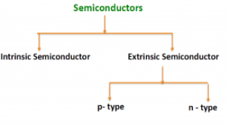
Figure 4: Type of semiconductor
The semiconductor is divided into two types. One is an Intrinsic Semiconductor and the other is an Extrinsic semiconductor. The pure form of the semiconductor is known as the intrinsic semiconductor and the semiconductor in which intentional impurities are added for making it conductive is known as the extrinsic semiconductor.
The conductivity of the intrinsic semiconductor becomes zero at room temperature while the extrinsic semiconductor is very little conductive at room temperature. The detailed explanation of the two types of the semiconductor is given below.
INTRINSIC SEMICONDUCTOR
An intrinsic type of semiconductor material made to be very pure chemically. As a result, it possesses a very low conductivity level having very few charge carriers, namely holes and electrons, which it possesses in equal quantities.

Figure 5: Intrinsic Semiconductor
The most commonly used semiconductor basics material by far is silicon. Silicon has four valence electrons in its outermost shell which it shares with its neighbouring silicon atoms to form a full orbital of eight electrons. The structure of the bond between the two silicon atoms is such that each atom shares one electron with its neighbour making the bond very stable.
As there are very few free electrons available to move around the silicon crystal, crystals of pure silicon (or germanium) are therefore good insulators. Silicon atoms are arranged in a definite symmetrical pattern making them a crystalline solid structure. A crystal of pure silica (silicon dioxide or glass) is generally said to be an intrinsic crystal (it has no impurities) and therefore has no free electrons.
An extremely pure semiconductor is called an Intrinsic Semiconductor. Based on the energy band phenomenon, an intrinsic semiconductor at absolute zero temperature is shown below.

Figure 6: Intrinsic semiconductor at absolute zero temperature.
Its valence band is filled and the conduction band is empty. When the temperature is raised and some heat energy is supplied to it, some of the valence electrons are lifted to the conduction band leaving behind holes in the valence band as shown below.

Figure 7: Intrinsic semiconductor at T >0
A hole is the absence of an electron in a particular place in an atom. Although it is not a physical particle in the same sense as an electron, a hole can be passed from atom to atom in a semiconductor material. It is considered to have a positive charge. Holes are positive charge carriers.
The electrons reaching the conduction band move randomly. The holes created in the crystal also free to move anywhere.
This behaviour of the semiconductor shows that they have a negative temperature coefficient of resistance. This means that with the increase in temperature, the resistivity of the material decreases, and the conductivity increases.
But simply connecting a silicon crystal to a battery supply is not enough to extract an electric current from it. To do that we need to create a “positive” and a “negative” pole within the silicon allowing electrons and therefore electric current to flow out of the silicon. These poles are created by doping the silicon with certain impurities.
DOPING
The process by which an impurity is added to a semiconductor is known as Doping. The amount and type of impurity which is to be added to the material have to be closely controlled during the preparation of extrinsic semiconductor. Generally, one impurity atom is added to 108 atoms of a semiconductor.
The purpose of adding impurity in the semiconductor crystal is to increase the number of free electrons or holes to make it conductive.
If a Pentavalent impurity, having five valence electrons is added to a pure semiconductor a large number of free electrons will exist. Which makes an n-type extrinsic semiconductor.
If a trivalent impurity having three valence electrons is added, a large number of holes will exist in the semiconductor. Which makes a p-type extrinsic semiconductor.
EXTRINSIC SEMICONDUCTOR
Extrinsic types of semiconductors are those where a small amount of impurity has been added to the basic intrinsic material. This 'doping' uses an element from a different periodic table group and in this way, it will either have more or fewer electrons in the valence band than the semiconductor itself. This creates either an excess or shortage of electrons. In this way two types of semiconductors are available: Electrons are negatively charged carriers. Holes are positively charged carriers.
Depending upon the type of impurity added the extrinsic semiconductor may be classified as an n-type semiconductor and p-type semiconductor.
P-TYPE EXTRINSIC SEMICONDUCTOR
The extrinsic p-Type Semiconductor is formed when a trivalent impurity is added to a pure semiconductor in a small amount, and as a result, a large number of holes are created in it. A large number of holes are provided in the semiconductor material by the addition of trivalent impurities like Gallium and Indium. Such type of impurities which produce a p-type semiconductor is known as an Acceptor Impurities because each atom of them creates one hole which can accept one electron.
In a P-type semiconductor material, there is a shortage of electrons, i.e. there are 'holes' in the crystal lattice. Electrons may move from one empty position to another and in this case, it can be considered that the holes are moving. This can happen under the influence of a potential difference and the holes can be seen to flow in one direction resulting in an electric current flow. It is harder for holes to move than for free electrons to move and therefore the mobility of holes is less than that of free electrons. Holes are positively charged carriers.
A trivalent impurity like Aluminium, having three valence electrons is added to Silicon crystal in a small amount. Each atom of the impurity fits in the Silicon crystal in such a way that its three valence electrons form covalent bonds with the three surrounding Silicon atoms as shown in the figure below.

Figure 8: p-Type Semiconductor
ENERGY BAND DIAGRAM OF P-TYPE SEMICONDUCTOR
The energy band diagram of a p-Type Semiconductor is shown below.

Figure 9: Energy band diagram of a p-Type Semiconductor
A large number of holes or vacant space in the covalent bond is created in the crystal with the addition of the trivalent impurity. A small or minute quantity of free electrons is also available in the conduction band.
They are produced when thermal energy at room temperature is imparted to the Silicon crystal-forming electron-hole pairs. But the holes are more in number as compared to the electrons in the conduction band. It is because of the predominance of holes over electrons that the material is called a p-type semiconductor. The word “p” stands for positive material.
CONDUCTION THROUGH P TYPE SEMICONDUCTOR
In p-type semiconductors, a large number of holes are created by the trivalent impurity. When a potential difference is applied across this type of semiconductors.

Figure 10: Conduction through p type semiconductor
The holes are available in the valence band are directed towards the negative terminal. As the current flow through the crystal is by holes, which are a carrier of positive charge, therefore, this type of conductivity is known as positive or p-type conductivity. In a p-type conductivity, the valence electrons move from one covalent to another.
The conductivity of an n-type semiconductor is nearly double that of a p-type semiconductor. The electrons available in the conduction band of the n-type semiconductor are much more movable than holes available in the valence band in a p-type semiconductor. The mobility of holes is poor as they are more bound to the nucleus.
Even at room temperature, the electron-hole pairs are formed. These free electrons which are available in minute quantity also carry a little amount of current in the p-type semiconductors.
N-TYPE EXTRINSIC SEMICONDUCTOR
When a few Pentavalent impurities such as Phosphorus whose atomic number is 15, which is categorized as 2, 8, and 5. It has five valence electrons, which are added to silicon crystals. Each atom of the impurity fits in four silicon atoms as shown in the figure below.
Hence, each Arsenic atom provides one free electron in Silicon crystal. Since an extremely small amount of Phosphorus, impurity has a large number of atoms; it provides millions of free electrons for conduction.
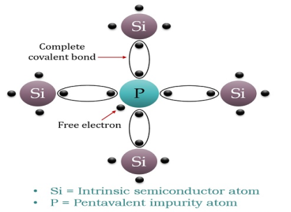
Figure 11: N-type semiconductor
An N-type semiconductor material has an excess of electrons. In this way, free electrons are available within the lattices, and their overall movement in one direction under the influence of a potential difference results in an electric current flow. This is an N-type semiconductor, the charge carriers are electrons.
ENERGY DIAGRAM OF N-TYPE SEMICONDUCTOR
A large number of free electrons are available in the conduction band because of the addition of the Pentavalent impurity. These electrons are free electrons that did not fit in the covalent bonds of the crystal. However, a minute quantity of free electrons is available in the conduction band forming hole- electron pairs.
The Energy diagram of the n-type semiconductor is shown in the figure below.

Figure 12: Energy diagram of the n-type semiconductor
- The addition of pentavalent impurity results in a large number of free electrons.
- When thermal energy at room temperature is imparted to the semiconductor, a hole-electron pair is generated and as a result, a minute quantity of free electrons is available. These electrons leave behind holes in the valence band.
- Here n stands for negative material as the number of free electrons provided by the pentavalent impurity is greater than the number of holes.
CONDUCTION THROUGH N-TYPE SEMICONDUCTOR
In the n-type semiconductor, a large number of free electrons are available in the conduction bands which are donated by the impurity atoms. The figure below shows the conduction process of an n-type semiconductor.
When a potential difference is applied across this type of semiconductor, the free electrons are directed towards the positive terminals. It carries an electric current. As the flow of current through the crystal is constituted by free electrons which are carriers of a negative charge, therefore, this type of conductivity is known as negative or n-type conductivity.
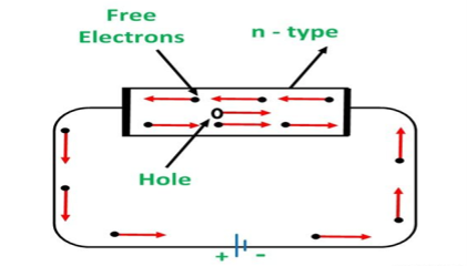
Figure 13: Conduction through n-type semiconductor
The electron-hole pairs are formed at room temperature. These holes which are available in small quantities in the valence band also consist of a small amount of current. For practical purposes, this current is neglected.
Key Takeaways
- Semiconductors are materials that have conductivity between conductors and insulators.
- The semiconductor is divided into two types. One is an Intrinsic Semiconductor and the other is an Extrinsic semiconductor.
- The pure form of the semiconductor is known as the intrinsic semiconductor
- The semiconductor in which intentional impurities are added for making it conductive is known as the extrinsic semiconductor.
- A hole is the absence of an electron in a particular place in an atom.
- The process by which an impurity is added to a semiconductor is known as Doping.
- Depending upon the type of impurity added the extrinsic semiconductor may be classified as an n-type semiconductor and p-type semiconductor.
- The extrinsic p-Type Semiconductor is formed when a trivalent impurity is added to a pure semiconductor in a small amount, and as a result, a large number of holes are created in it.
- The extrinsic n-Type Semiconductor is formed when a Pentavalent impurity is added to a pure semiconductor in a small amount, and as a result, a large number of electrons are created in it.
FERMI LEVEL IN INTRINSIC
Intrinsic semiconductors—carrier concentration
Here we will calculate the number of electrons excited into the conduction band at temperature T and also the hole concentration in the valence band. It is assumed that the electrons in the conduction band behave as if they are free particles with effective mass me* and the holes near the top of the valence band behave as if they are free particles with effective mass mh*.
Here we will calculate the electron concentration, hole concentration
The density of Electrons in Conduction Band
The number of free electrons per unit volume of a semiconductor having energies in between E and E + dE is represented as N(E) dE
dE = width of Energy band
Therefore, we have:
N(E) dE = ge(E) dE fe(E) ……….(1)
ge(E) = The density of electron states per unit volume
fe(E) = Fermi-Dirac distribution function i.e. probability that an electron occupies an electron state
The number of electrons present in the conduction band per unit volume of material ‘n’ is obtained by integrating N(E) dE between the limits Ec and Ect
Where Ec = the bottom energy levels of the conduction band
Ect = the bottom and top energy levels of the conduction band
n =  ……….(2)
Can be written as
n =  =
= 
n =  -
-  ……….(3)
We know that above Ect, there are no electrons.
Hence, Equation (3) becomes
n =  -
- 
n =  ……….(4)
The Fermi-Dirac distribution function fe(E) can be represented as:
 (E) =
(E) = ……….(5)
Compared to the exponential value, so the ‘1’ in the denominator can be neglected.
So  >>1
>>1
Hence,  (E) =
(E) = =
=  ……….(6)
The density of electron states ge(E) in the energy space from E = 0 to E can be written as:
 (E) =
(E) =  [
[ ]3/2 (E - 0) ½ ……….(7)
Where me* is the effective mass of an electron and h is Planck’s constant.
 (E)dE =
  [
[ ]3/2 (E - 0) ½dE ……….(8)
To evaluate n, the density of states is counted from Ec, since the minimum energy state in the conduction band is Ec. So eq (8) can become
 (E)dE =
  [
[ ]3/2 (E - Ec) ½dE ……….(9)
Substituting Equations (6) and (9) in (4) gives
n =  3/2
3/2 (E-
(E- )1/2
)1/2 dE
dE
n = [
[ ]3/2
]3/2  1/2
1/2 dE ………… (10)
The above equation can be simplified by the following substitution:
Put ɛ = E − Ec ………… (11)
So, dɛ = dE
In Equation (11), Ec is constant, as we change the variable E to ε in Equation (10), the integral limits also change.
In Equation (11), as E → Ec then ε → 0 and E → ∞, then ε also → ∞.
The exponential term in Equation (10) becomes:
 = exp [
 ] = exp [
 ]
]

 ………… (12)
Substituting Equations (11) and (12) in (10), we get:
n = [
[ ]3/2
]3/2  dE
dE
n = [
[ ]3/2
]3/2
 dE ………… (13)
Above integral (I) can be simplified by substitution. Put ε = x2
So that dɛ = 2x dx
I = 2x dx
2x dx
= dx
dx
= =
= T)3/2 ………… (14)
Substituting Equation (14) in (13) gives:
n = [
[ ]3/2
]3/2 T)3/2
T)3/2
n =
n = 
n =  ………… (15)
The term  is almost a constant compared with the exponential term as the temperature changes. So, it is a pseudo constant and is given by the symbol Nc. So, we have
n =Nc ………… (16)
The density of Holes in Valence Band
The number of holes per unit volume of semiconductor in the energy range E and E + dE in the valence band is represented as P(E) dE. Proceeding the same way (as in the case of electrons) we have
Therefore, we have:
P(E) dE = gh(E) dE fh(E) ……….(17)
dE = width of Energy band
gh(E) = The density of holes states per unit volume
fh(E) = Fermi-Dirac distribution function i.e. probability that a hole occupies an electron state
The number of electrons present in the conduction band per unit volume of material ‘n’ is obtained by integrating P(E) dE between the limits Evb and EV
Where EV = the bottom energy levels of the valence band
Evb = the bottom and top energy levels of the valence band
The total number of holes present in the valence band per unit volume of material ‘p’ is obtained by integrating P(E) dE  ……….(18)
Equation (18) can be represented as:
 ……….(19)
Now we know that below Evb no holes are present. Hence, Equation(19) becomes
 ……….(20)
We know a hole can also be defined as the absence of an electron.
Presence of a hole = the absence of an electron
Hence, the Fermi-Dirac function of holes fh(E) in the valence band is:
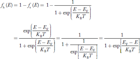
Compared to exponential, the ‘1’ in the denominator is negligible,

Hence,
 ……….(21)
The density of hole states between E and E + dE in valence band can be written similar to Equation (8.9) for electrons.
 ……….(22)
Where mh* is the effective mass of the hole.
Substituting Equations (21) and (22) in (20),
 ……….(23)
The above equation can be simplified by the substitution:
Put ɛ = EV − E ............. (24)
So dɛ = − dE
In Equation (24), EV is constant, as we change the variable E to ε in Equation (23), the integral limits also change.
In Equation (24),
As E → EV then ε → 0
And E→ −∞, then ε → ∞
The exponential term in Equation (23) becomes:
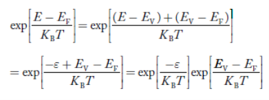 ............. (25)
Substituting Equations (24) and (25) in (23), we get:
 ………….(26)
From Equation (14), we know the integral value  T)3/2 put here and we get
 ………….(27)
….The term  is almost constant compared with the exponential term as the temperature changes. So, it is a pseudo constant and is given by the symbol NV. So, we have
 …………… (28)
Fermi Level
We know that in an intrinsic semiconductor
Electron concentration ‘n’ = Hole concentration ‘p’
Equating Equations (15) and (27), we get
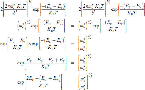
Taking logarithms on both sides, we get
 ……………… (29)
Normally, mh* is greater than me*, since ln  is very small so that EF is just lie in the middle of the energy gap
Temperature effect on Fermi level
Fermi level slightly rises with an increase of temperature.
But in the case of a pure intrinsic semiconductor like Si and Ge,
mh* ≈ me*
So in these cases, the Fermi level lies in the middle of the energy gap.
FERMI LEVEL IN EXTRINSIC SEMICONDUCTORS
Dependence of fermi energy on carrier concentration and temperature (qualitative)-
Carrier Concentration in Extrinsic Semiconductors
The number of charge carriers presents per unit volume of a semiconductor material is called carrier concentration.
Suppose donor and acceptor atoms are doped in a semiconductor.
At temperature T K,
n = number of conduction electrons
p = number of holes
N−A = number of acceptor ions
N+D = number of donor ions
We know that the below equation holds good in the semiconductor. The total negative charge due to conduction electrons and acceptor ions is equal to holes and donor ions in a unit volume of material.
So the material will be considered neutral if,
n + N−A = p + N+D ……….(34)
Equation (34) is called the charge neutrality equation.
In the above equation
 ………..(35)
Concentration of acceptor ions N−A = acceptor concentration x probability of finding an electron in acceptor level
 ………..(36)
Similarly, the donor ions concentration is

 ………..(37)
In n-type material
Note
nn represents electrons in n-type material
pn represents holes concentration in n-type material.
There are no acceptor atoms so N−A = 0.
At 0 K, all the electron states at the donor level are occupied by electrons.
As the temperature is increased from 0 K, some of the electrons jump from these donor states into the conduction band.
Also, the concentration of holes is extremely less compared with the concentration of conduction electrons [p << n]
From Equation (34) we have
n = p N+D
(Or) n ≈ N+D …………(38) [since p << N+D]
At temperature T K,
As the temperature increase, almost all the donor atoms donate electrons to the conduction band.

Figure 14: Energy level diagram of N type semiconductor
So, in n-type material, the free electron concentration is almost equal to the donor atoms.
So we can rewrite the above equation as
nn ≈ ND …………….(39)
Where nn represents electrons in n-type material
Also, the hole concentration in n-type material can be obtained by applying the law of mass action nn pn =ni2
 …………..(40)
Where pn represents holes concentration in n-type material.
In n-type material at 0 K, the Fermi energy level lies in the middle of Ec and ED

At temperature> 0K
 ……….(41)
With the increase in temperature, the Fermi level shifts upwards according to Equation (61) slightly due to the ionization of donor atoms.
With further increase of temperature, electron-hole pairs are generated due to the breaking of covalent bonds, hence Fermi level shifts downwards.
In p-type semiconductor
Note
pp represents holes in the p-type material
np represents electrons in the p-type material
There are no donor atoms so means no ions present  = 0.
= 0.
At 0 K, all the acceptor levels are not occupied by electrons.
As the temperature is increased from 0 K, some electrons jump from top valence band energy levels to the acceptor states, leaving holes in the valence band and acceptor ions  are formed.
At some room temperature T K, the concentration of conduction electrons is extremely less compared with hole concentration.
∴ From Equation (34), we have
n + N−A = p ……………(42)
(or) N−A ≈ p ……………. (43) [since n << N−A]
At temperature T K, in p-type material,
The hole concentration is almost equal to the acceptor atoms in a unit volume of the material.
So, Equation (43) can be written as
pp ≈ NA ……………….(44)
Where pp represents holes in the p-type material
The electron concentration in p-type material can be obtained by applying the law of mass action as nppp = ni2
 …………….(45)
Where np represents free electron concentration in the p-type material.
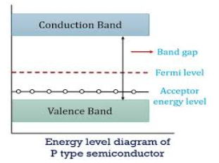
Figure 15: Energy level diagram of N type semiconductor.
In p-type material, the Fermi level lies in between EV and EA at 0 K

As the temperature is increased from 0 K, the Fermi level shifts downwards slightly as per Equation (46) due to ionization of acceptor atoms.
And with a further increase of temperature, electron-hole pairs are generated due to the breaking of covalent bonds, so the Fermi level shifts upwards.
Key Takeaways
- The density of Electrons in Conduction Band
n =Nc
- The density of Holes in Valence Band

- Fermi level slightly rises with an increase of temperature. But in the case of a pure intrinsic semiconductor like Si and Ge, mh* ≈ me*, So in these cases, the Fermi level lies in the middle of the energy gap.
- Carrier Concentration in Extrinsic Semiconductors
- The donor ions concentration is

- Concentration of acceptor ions N−A

- Fermi Level shifts in case of extrinsic semiconductor.
Hall Effect
When the magnetic field is applied perpendicular to a current-carrying conductor, then a voltage is developed in the material perpendicular to both the magnetic field and current in the conductor. This effect is known as Hall Effect and the voltage developed is known as Hall voltage (VH).
Hall Effect is useful to identify the nature of charge carriers in material and hence to decide whether the material is an n-type semiconductor or p-type semiconductor, also to calculate carrier concentration and mobility of carriers.
Hall Effect can be explained by considering a rectangular block of an extrinsic semiconductor in which current is flowing along the positive X-direction and magnetic field B is applied along Z-direction as shown in Figure.

Figure 16: Hall Effect
Suppose if the semiconductor is n-type, then mostly the carriers are electrons and the electric current is due to the drifting of electrons along negative X-direction or if the semiconductor is p-type, then mostly the carriers are holes and the electric current is due to drifting of the holes along positive X-direction.
As these carriers are moving in the magnetic field in the semiconductor that means they experience Lorentz force represented by FL
FL = Bevd
Where vd is the drift velocity of the carriers. (already explained in the previous section).
We can obtain the direction of this force by applying Fleming’s left-hand rule in electromagnetism.
Fleming’s left-hand rule can be explained as If we stretch the thumb, forefinger, and middle finger in three perpendicular directions so that the forefinger is parallel to the magnetic field and the middle finger is parallel to the current direction, then the thumb represents the direction of the force on the current-carrying carriers.
So the Lorentz force is exerted on the carriers in the negative Y-direction. Due to Lorentz force, more and more carriers will be deposited at the bottom face (represented by face 1in the figure) of the conductor.
The deposition of carriers at the bottom face is continued till the repulsive force due to accumulated charge balances the Lorentz force.
After some time of the applied voltage, both the forces become equal in magnitude and act in opposite direction, then the potential difference between the top and bottom faces is equal to Hall voltage and that can be measured.
At equilibrium, the Lorentz force on a carrier
FL = Bevd ……………..(1)
And the Hall force
FH = eEH ……………..(2)
Where EH is the Hall electric field due to accumulated charge.
At equilibrium, FH = FL
EEH = Bevd
∴ EH = Bvd ……………..(3)
If ‘d’ is the distance between the upper and lower surfaces of the slab, then the Hall field
EH =  ……………..(4)
In n-type material, Jx = –nevd
vd = -  ……………..(5)
Where n is free electron concentration, substituting (5) in (3), we have
∴ EH = -B  ……………..(6)
For a given semiconductor, the Hall field EH is proportional to the current density Jx and the intensity of magnetic field ‘B’ in the material.
i.e. EH ∝ JxB
(or) EH = RHJxB ……………..(7)
Where RH = Hall coefficient
Equations (6) and (7) are the same so, we have
RHJxB =-B 
RH = -  = -
= -  ……………..(8)
Where ρ is the charge density
Similarly for p-type material
RH =  =
= ……………..(9)
Using Equations (8) and (9), carrier concentration can be determined.
Thus, the Hall coefficient is negative for n-type material. In n-type material, as the more negative charge is deposited at the bottom surface, so the top face acquires positive polarity and the Hall field is along negative Y-direction. The polarity at the top and bottom faces can be measured by applying probes.
Similarly, in the case of p-type material, a more positive charge is deposited at the bottom surface. So, the top face acquires negative polarity and the Hall field is along positive Y-direction. Thus, the sign of the Hall coefficient decides the nature of (n-type or p-type) material.
The Hall coefficient can be determined experimentally in the following way:
Multiplying Equation (7) with ‘d’, we have
EHd = VH = RHJxBd ……………..(10)
From (Figure 16) we know the current density Jx
Jx = 
Where W is the width of the box. Then, Equation (10) becomes
VH = RH Bd = RH
RH =  ……………..(11)
Substituting the measured values of VH, Ix, B, and W in Equation(11), RH is obtained. The polarity of VH will be the opposite for n- and p-type semiconductors.
The mobility of charge carriers can be found by using the Hall effect, for example, the conductivity of electrons is
n = neμn
Or we can rewrite it as
μn =  =n RH ……………..(12)
By using equation (11)
μn = n ……………..(13)
Applications of Hall Effect
• Using magnetic flux leakage – To properly inspect items such as pipes or tubes, Hall Effect probes work with something called magnetic flux leakage. This is a way of testing such items, and being able to spot potential corrosion, erosion, or pitting. This is specifically used in steel items and can give important information about lifespan or safety.
• Sensors to detect rotation speed – A Hall Effect probe can be used in bicycle wheels, speedometers in the automotive world, electronic types of ignition systems, and gear teeth.
• Used to detected movement – You will often find a Hall Effect probe used in such items as Go-Kart controls, smartphones, paintball guns, or airsoft guns, as well as some GPS systems.
• Ferrite Toroid Hall Effect current transducers – This is mainly used in electronic compasses, making use of the magnetic field to show direction.
• Split-ring clamp-on sensors – These types of Hall Effect probes are used to test equipment without having to take the whole circuit board apart, e.g. Complex items.
• Analog multiplication – Anything which needs a power measurement, e.g. Sensing, and is also used in small computers.
• General power measurement – Any device which needs to be tested for its power input can be done by a Hall Effect probe.
• Position and motion sensors – This is mainly used in a DC motor, often the brushless type.
• The automotive world – Hall Effect probes are used widely in the automotive world, especially in fuel injection and ignition. Wheel rotation sensors also use Hall Effect probes, e.g. For anti-lock braking.
- For determination of the type of given semiconductor.
- For N-type, Hall coefficient RH= negative
- For P-type, Hall coefficient RH= Positive
- To determine carrier concentration n and p; that is n=p=1/e𝑅𝐻
- Determination of mobility of charge carriers μn =
 =n RH. Where 𝜎= electrical conductivity
 - To determine the sign of charge carriers whether the conductivity is due to electrons or holes.
Main Advantages of Using Hall Sensors
Why is a Hall Effect probe advantageous in all of these instances? Because the probes are not affected by outside influences, e.g. Water or dirt. They can also easily sense the measure of the output they need when they are placed in the right position. On top of this, Hall Effect probes are safer, because the voltage never actually makes it directly to the sensor/probe. This makes this type of measurement overall so much safer than other methods.
As you can see, understanding how something is put into practice in the real world helps you to understand it in real terms. The Hall Effect is certainly very commonplace these days, in much more methods and applications than we realize. While certainly very useful in the automation world, even basic items such as a compass make large use of this scientific approach.
Key Takeaways
- When the magnetic field is applied perpendicular to a current-carrying conductor, then a voltage is developed in the material perpendicular to both the magnetic field and current in the conductor. This effect is known as Hall Effect.
- The voltage developed is known as Hall voltage (VH).
- Hall Effect is useful to identify the nature of charge carriers in material and hence to decide whether the material is an n-type semiconductor or p-type semiconductor.
- Hall Effect also to calculate carrier concentration and mobility of carriers.
- Hall coefficient is given by RH = -
 = -
= -  Where ρ is the charge density
 - Hall coefficient is given by RH =

- Mobility of charge carriers can be found by using the Hall Effect μn = n

Q1) The Hall coefficient of certain silicon specimen was found to be –7.35 × 10⁻⁵ m3 C–1 from 100 to 400 K. Determine the nature of the semiconductor. If the conductivity was found to be 200 –1 m–1. Calculate the density and mobility of the charge carrier.
A 1)
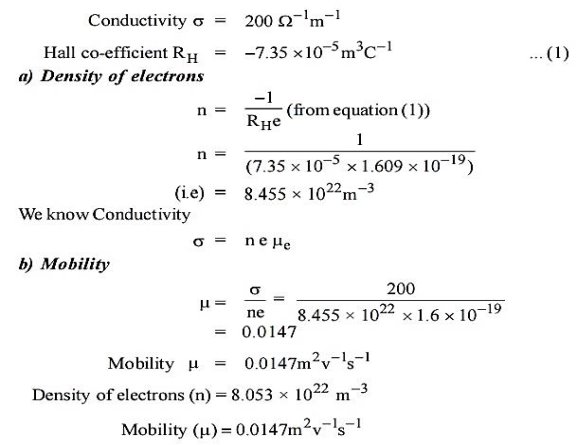
Q 2) An N-type semiconductor has hall coefficient = 4.16 × 10⁻⁴ m3 C–1. The conductivity is 108 m–1. Calculate its charge carrier density ‘ne’and electron mobility at room temperature.
A 2)
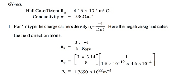

Q 3) In an N-type semiconductor, the concentration of electron is 2 × 10²² m–3. Its electrical conductivity is 112 m–1. Calculate the mobility of electrons.
A 3)
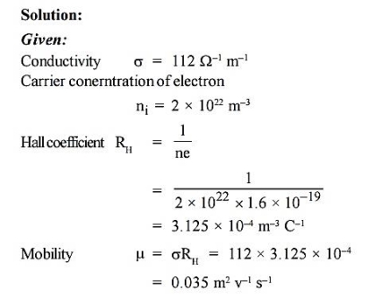
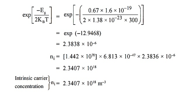
Q 4) Calculate the intrinsic concentration of charge carriers at 300 K given that m *e =0.12m o ,m *h =0.28mo and the value of brand gap = 0.67 eV.
A 4)

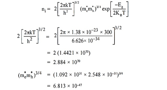
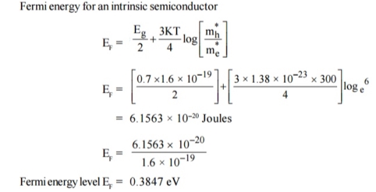
Q5) For an intrinsic Semiconductor with a band gap of 0.7 eV, determine the position of EF at T = 300 K if m*h = 6m*e
A5)

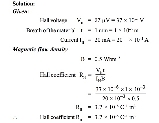
Q 6) A semiconducting crystal with 12 mm long, 5 mm wide and 1 mm thick has a magnetic density of 0.5 Wbm–2 applied from front to back perpendicular to largest faces. When a current of 20 mA flows length wise through the specimen, the voltage measured across its width is found to be 37μV . What is the Hall coefficient of this semiconductor?
A 6)
Reference Books
- Principle of electronics S. Chand V K Mehta and Rohit Mehta
- A textbook of Engineering Physics, Dr. M. N. Avadhanulu, Dr. P.G. Kshirsagar - S.Chand
- Engineering Physics, R.K. Gaur and S.L. Gupta, Dhanapat Rai Publications