UNIT 3
Introduction to Solids
- This theory was developed by Lorentz and Drude in 1990.
- In metals there are large number of free electrons moving freely in all possible directions.
- The assumption is made that free electrons in metals behave like gas molecule obeying kinetic theory of gases.
- In metals electrons move randomly and collide with either +ve ions or free electrons accelerated in opposite direction to the applied.
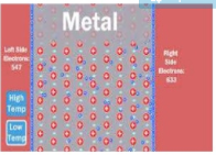
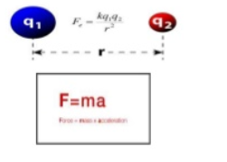
Figure 1. Free electron theory
Quantum free electron theory
In 1928, Sommerfeld developed a new theory applying quantum mechanical concepts and Fermi-Dirac statistics to the free electrons in the metal. This theory is called quantum free electron theory.
Classical free electron theory permits all electrons to gain energy. But quantum free electron theory permits only a fraction of electrons to gain energy.
In order to determine the actual number of electrons in a given energy range(dE), it is necessary to know the number of states(dNs) which have energy in that range. The number of states per unit energy range is called the density of states g(E).
Therefore, g(E) = dNs/dE.
According to Fermi-Dirac statistics, the probability that a particular energy state with energy E is occupied by an electron is given by,
f(E) = 1 / [1+e(E-EF/KT) ]
where EF is called Fermi level. Fermi level is the highest filled energy level at 0 K.
Energy corresponding to Fermi level is known as Fermi energy. Now the actual number of electrons present in the energy range dE,
dN = f(E) g(E)dE
The probability of occupation of energy levels in valence band and conduction band is called Fermi level. At absolute zero temperature intrinsic semiconductor acts as perfect insulator. However as the temperature increases electrons and holes are generated.
In intrinsic or pure semiconductor, the number of holes in valence band is equal to the number of electrons in the conduction band.
Hence, the probability of occupation of energy levels in conduction band and valence band are equal. Therefore, the Fermi level for the intrinsic semiconductor lies in the middle of forbidden band.
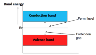
Figure Intrinsic semiconductor
Fermi level in the middle of forbidden band indicates equal concentration of free electrons and holes.
The hole-concentration in the valence band is given as

The electron-concentration in the conduction band is given as

Where KB is the Boltzmann constant
T is the absolute temperature of the intrinsic semiconductor
Nc is the effective density of states in the conduction band.
Nv is the effective density of states in the valence band.
The number of electrons in the conduction band is depends on effective density of states in the conduction band and the distance of Fermi level from the conduction band.
The number of holes in the valence band is depends on effective density of states in the valence band and the distance of Fermi level from the valence band.
For an intrinsic semiconductor, the electron-carrier concentration is equal to the hole-carrier concentration.
It can be written as
p = n = ni
Where P = hole-carrier concentration
n = electron-carrier concentration
And ni = intrinsic carrier concentration
The fermi level for intrinsic semiconductor is given as,

Where EF is the fermi level
EC is the conduction band
EV is the valence band
Therefore, the Fermi level in an intrinsic semiconductor lies in the middle of the forbidden gap.
Fermi level in extrinsic semiconductor
In extrinsic semiconductor, the number of electrons in the conduction band and the number of holes in the valence band are not equal. Hence, the probability of occupation of energy levels in conduction band and valence band are not equal. Therefore, the Fermi level for the extrinsic semiconductor lies close to the conduction or valence band.
Fermi level in n-type semiconductor
In n-type semiconductor pentavalent impurity is added. Each pentavalent impurity donates a free electron. The addition of pentavalent impurity creates large number of free electrons in the conduction band.
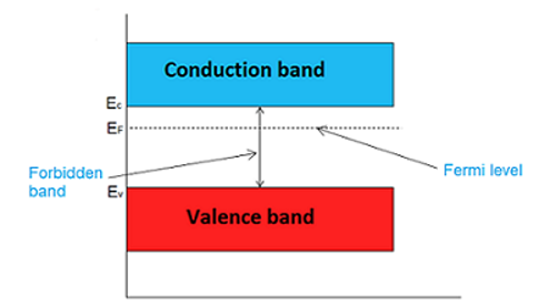
Figure Extrinsic semiconductor
At room temperature, the number of electrons in the conduction band is greater than the number of holes in the valence band.
Hence, the probability of occupation of energy levels by the electrons in the conduction band is greater than the probability of occupation of energy levels by the holes in the valence band.
This probability of occupation of energy levels is represented in terms of Fermi level. Therefore, the Fermi level in the n-type semiconductor lies close to the conduction band.
The Fermi level for n-type semiconductor is given as

Where EF is the fermi level.
EC is the conduction band.
KB is the Boltzmann constant.
T is the absolute temperature.
NC is the effective density of states in the conduction band.
ND is the concentration of donar atoms.
Fermi level in p-type semiconductor
In p-type semiconductor trivalent impurity is added. Each trivalent impurity creates a hole in the valence band and ready to accept an electron. The addition of trivalent impurity creates large number of holes in the valence band.
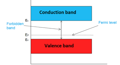
Figure p-type semiconductor
At room temperature, the number of holes in the valence band is greater than the number of electrons in the conduction band.
Hence, the probability of occupation of energy levels by the holes in the valence band is greater than the probability of occupation of energy levels by the electrons in the conduction band.
This probability of occupation of energy levels is represented in terms of Fermi level. Therefore, the Fermi level in the p-type semiconductor lies close to the valence band.
The Fermi level for p-type semiconductor is given as

Where NV is the effective density of states in the valence band.
NA is the concentration of acceptor atoms.
The density of states (DOS) is fundamentally the number of dissimilar states at a specific energy level that electrons are allowable to occupy, i.e. the amount of electron states for each unit volume for each unit energy.
Majority things such as specific heat, paramagnetic susceptibility and additional transport singularities of conductive solids depend on this meaning.
DOS calculations agree one to regulate the general supply of states as a function of energy and can also govern the spacing amid energy bands in semi-conductors.
Density of States for Waves
Before we get involved in the derivation of the DOS of electrons in a material, it may be easier to first consider just an elastic wave propagating through a solid.
Elastic waves are in orientation to the lattice vibrations of a solid included of distinct atoms. However, when the wavelength is very long, the atomic nature of the solid can be unnoticed and we can treat the material as a constant medium.
We start by the 1-D wave calculation:
With which we then have a answer for a propagating plane wave:  (1)
(1)
q= wave number ,
,
A=amplitude,
ω = frequency,
Vs = velocity of sound
Dispersion Relation:

In equation (1), the activist factor,  can be absent because it is not relevant to the derivation of the DOS [2].
So now we will use the answer: (2)
(2)
To start, we must apply some type of boundary circumstances to the organization.
The easiest way to do this is to reflect a periodic boundary circumstance.
Through a periodic limit condition, we can visualize our system requiring two ends, one being the origin 0 and the other L.
We now say that the origin end is unnatural in a way that it is always at the similar state of oscillation as end L [2].
This boundary state is signified as:
Now we relate the boundary state to equation (2) to acquire:
Now, spending Euler’s individuality;  we can see that there are firm values of qL which fulfil the above equation.
Those standards are  for any integer, n. Leaving the relation:
If you choose integer standards for n and design them along an axis q you get a 1-D line of points, known as modes, with a spacing of  amid each mode.
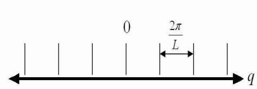

We now have that the number of modes in an interval dq in q-space equals:

By means of the dispersion relation we can find the number of modes inside a frequency range dω that lies inside .
.
This number of modes in that range is signified by g(ω)dω , where gω is demarcated as the density of states.
So now we get that g(ω)dω = which
which
We go into:
We do so in order to practice the relation:
And
Get:
we grow by a factor of two since there are modes in positive and negative q-space, and we acquire the density of states for a phonon in 1-D:

2-D:
We can now originate the density of states for two dimensions.
Equation (2) becomes: now apply the same boundary circumstances as in the 1-D case:


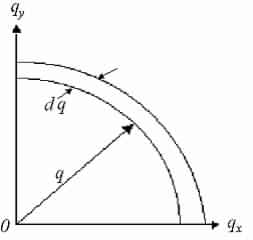
We now study an area for each point in q-space =(2π/L)2 and discovery the number of modes that lie inside a flat ring with thickness dq, a radius q and area:
Number of modes inside intermission:
Now explanation for transverse and longitudinal modes (multiply by a factor of 2) and set equivalent to g(ω)dω
We get  and
and
Apply dispersal
Relation to get  which make
Simpler to the 2-D result:

3-D:
We can now derive the density of states for three dimensions.
Equation(2) develops:
Now apply the same boundary conditions as in the 1-D case to become:
We now study a volume for to each point in q-space =(2π/L)3 and discovery the number of modes that lie within a spherical shell, thickness dq, with a radius q and volume:4/3πq3
Number of modes inside shell:
Supposing a common velocity for transverse and longitudinal waves we can explanation for one longitudinal and two transverse modes for each value of q (multiply by a factor of 3) and set equal to g(ω)dω:
Apply dispersal relative and let L3=V to get  and shorten for the 3-D result:

Bloch's Theorem
Until now, approaches to quantum mechanics to solve the problem of many bodies have been discussed.
However, the correlated nature of the electrons within a solid is not the only obstacle to solving the Schrödinger equation for a condensed matter system: for solids, the really infinite number of electrons within the solid must also be taken into account
Bloch's theorem can be used to advance in solving the last problem. Instead of having to consider an infinite number of electrons, it is necessary to consider only the number of electrons within the unit cell (or half of this number if the electrons are spin degenerate).
Bloch's theorem states that the wave function of an electron within a perfectly periodic potential can be written as

Where  is a function that keeps the periodicity of the
Potential, i.e.  , where
  is the length of the unit cell. In i is the band index, and
  is a wavevector kept to the first Brillouin Region. Meanwhile
  is a periodic function, we may enlarge it in terms of a Fourier sequence:

Where they  are mutual lattice vectors defined through
  , where m is an integer,
  is a real space lattice vector and the
  are plane wave development coefficients.
The electron wavefunctions may so be written as a linear mixture of plane waves:

Since each electron occupies a defined state, the infinite number of electrons within the solid generates an infinite number of k points. At each point k, only a finite number of available energy levels will be occupied.
Therefore, it is sufficient to consider a finite number of electrons at an infinite number of points k.
This may appear to replace one infinity (number of electrons) with another (number of k points) with a discrete advantage.
However, it is not necessary to consider all these k points; rather, since the wave functions of the electron will be almost identical for values close enough, one can represent the wave functions in a region of reciprocal space by considering the wave function at a single point k.
Therefore, it is sufficient to consider the electronic states at a finite number of points k to determine the solid-state density of the solid.
The net effect of Bloch's theorem was, therefore, to change the problem of an infinite number of electrons into one to consider only the number of electrons in the unit cell (or half of that number, depending on whether the states are degenerate by rotation or less) to a finite number of k points chosen to adequately sample the Brillouin area; This problem returns later.
The Kronig-Penney model is a shortened model for an electron in a one-dimensional periodic possible. The imaginable states that the electron can inhabit are firm by the Schrödinger equation,

In the case of the Kroning-Penney model, the potential V(x) is a periodic square wave.
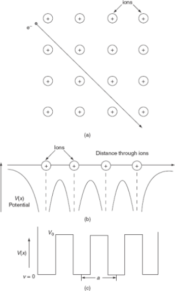
A feature of this model is that it is thinkable to systematically control the energy eigenvalues and eigenfunctions. It is also likely to discovery analytic terms for the diffusion relation (E vs. k) and the electron density of states.
The energies of the electrons can be known by solving the Schrödinger wave equation in this network. Schrödinger's time independent wave equation for the motion of an electron along the X direction is given by:
 ...............(1)
The electron energies and wave functions associated with this model can be calculated by solving the time-independent one-dimensional Schrödinger wave equations for the two regions I and II, as shown in Fig. Schrödinger's equations are: for 0<x<a.............(2)
 for -b<x<0.............(3)
We define two real quantities (say) α and β such that:

Hence, Equations (5.41) and (5.42) becomes:
 for 0<x<a
 for -b<x<0
According to Bloch's theorem, the solution of the wave function of the Schrödinger equation when the potential is periodic and to make sure that the function u (x) is also continuous and regular, can be written as:

Where u(x) is a periodic function which fulfills u(x + a) = u(x).
Using Bloch theorem and all the periphery circumstances for the stability of the wave meaning the answer of Schrodinger wave equation got as

Where,

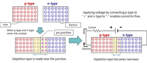
Definition: A p-n junction is an interface or a boundary between two semiconductor material types, namely the p-type and the n-type, inside a semiconductor.
p type semiconductor have hole as majority carrier while minority carrier electron
similarly n type have majority electron and minority carrier hole
When p-type and n-type come into contact depletion layer is made near the junction.
Connecting battery positive terminal at p type and n type then we can get narrower depletion layer this kind of bias is known as forward bias while after changing terminal we can get reverse bias.
Flow of electron and current are opposite to each other.
Metal-Semiconductor Junction (Ohmic And Schottky):
Whenever a metal and a semiconductor come together, there emerging of a potential barrier between the two that prevents most charge electrons or holes from passing from one to the other.
Small number of carriers has the energy to get over out of material.
When a bias is applied to the junction either it can make the barrier seem lower from the semiconductor side, or it can make it appear higher.
The bias neither changes the barrier height from the metal side.
Finally, this is a Schottky Barrier (rectifying contact), where the junction conducts for one bias polarity, but not the other.
About all metal-semiconductor junctions exhibit some of this rectifying performance.
Schottky Contacts make good diodes and may even be used to make a sympathetic of transistor, but for getting signals into and out of a semiconductor device, we are interested in Ohmic contacts.
Ohmic contacts conduct the same for both polarities (negative and positive). (They follow Ohm's Law).
There are two ways to make a metal-semiconductor contact look ohmic enough to get signals into and out of a semiconductor (or doing the opposite makes a good Schottky contact).
Lower the barrier height
We will use those materials whose barrier height is minor.
Strengthening may form an alloy between the semiconductor and the metal at the junction, which can also inferior the barrier height.
Make the barrier very narrow
One very interesting property of very tiny particles like electrons and holes is that they can "tunnel" through barriers that they don't have sufficient energy to just pass over.
The probability of tunnelling becomes high for very thin barriers .
We make the barrier actual thinnest by doping it very heavily (1019 dopant atoms/cm3 or more).
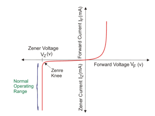
- Zener diode is a special type of p-n junction semiconductor diode in this diode the reverse breakdown voltage is adjusted precisely between 3v to 200v.
- Its applications are based on this principle hence Zener diode is called as a breakdown diode.
- The doping level of the imparity added to manufacture the zener diode is controlled in order to adjust the precise value of breakdown voltage.
PRINCIPLE OF OPERATION: - A zener diode can be forward biased or reverses biased. Its operation in the forward biased mode is same as that of a p-n junction diode but its operation in the reverse biased mode is sustainably deferent.

Numerical:
A 5.0V stabilized power supply is required to be produced from a 12V DC power supply input source. The maximum power rating PZ of the zener diode is 2W. Using the zener regulator circuit above calculate:
a). The maximum current flowing through the zener diode.
Maximum current = Watts/ Voltage =2W/5V =400mA
b). The minimum value of the series resistor, RS
 = 17.5 Ω
c). The load current IL if a load resistor of 1kΩ is connected across the zener diode.

d). The zener current IZ at full load.
Iz =Is -Il =440mA – 5mA = 395mA
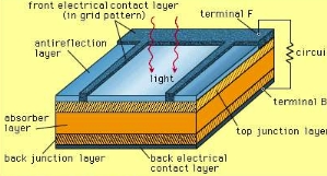
Definition: Solar cell, also called photovoltaic cell, any device that directly changes the energy of light into electrical energy through the photovoltaic effect.
The irresistible majority of solar cells are fabricated from silicon—with cumulative efficiency and lowering cost as the materials range from amorphous (nanocrystalline) to polycrystalline to crystalline (single crystal) silicon forms.
Unlike batteries or fuel cells, solar cells do not utilize chemical reactions or require fuel to produce electric power and unlike electric generators they do not have any affecting parts.
|
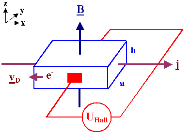
| The Hall effect describes what happens when current flows through a conducting material such as a metal or semiconductor, when exposed to a magnetic field B. | |||||||||||||||||||||||||||||||||||||||||||||||||||||||||||||||
|
| ||||||||||||||||||||||||||||||||||||||||||||||||||||||||||||||||
|
|
Figure . Hall effect
|
|
| |||||||||||||||||||||||||||||||||||||||||||||||||||||||||||||
|
|
|
| ||||||||||||||||||||||||||||||||||||||||||||||||||||||||||||||
|
|
|
| ||||||||||||||||||||||||||||||||||||||||||||||||||||||||||||||
|
|
|
| ||||||||||||||||||||||||||||||||||||||||||||||||||||||||||||||
| a
| ||||||||||||||||||||||||||||||||||||||||||||||||||||||||||||||||
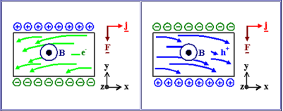 | |||||||||||||||||||||||||||||||||||||||||||||||||||||||||||||||||
Figure Charge carriers
| |||||||||||||||||||||||||||||||||||||||||||||||||||||||||||||||||
| |||||||||||||||||||||||||||||||||||||||||||||||||||||||||||||||||
| |||||||||||||||||||||||||||||||||||||||||||||||||||||||||||||||||
