Unit - 4
Peripheral devices and their characteristics
I/O devices are very important in computer systems. They provide users the means of interacting with the system. So there is a separate I/O system devoted to handling the I/O devices.
The different Components of the I/O systems are −
I/O Hardware
There are many I/O devices handled by the operating system such as a mouse, keyboard, disk drive, etc. Different device drivers can be connected to the operating system to handle a specific device. The device controller is an interface between the device and the device driver.
A diagram to represent this is −
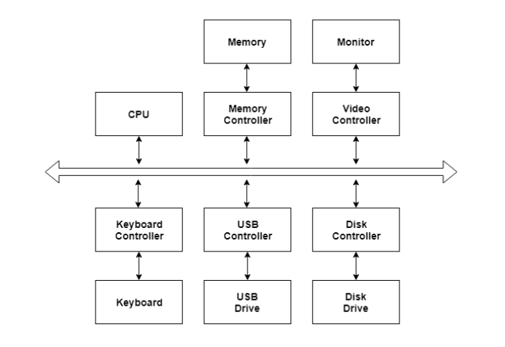
Fig 1 – I/O hardware
I/O Application Interface
The user applications can access all the I/O devices using the device drivers, which are device-specific codes. The application layer sees a common interface for all the devices.
This is illustrated using the below image −
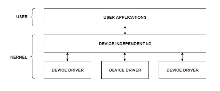
Fig 2 – I/O application interface
Most of the devices are either block I/O and character I/O devices. Block devices are accessed one block at a time whereas character devices are accessed one character at a time.
I/O Software
The I/O software contains the user-level libraries and the kernel modules. The libraries provide the interface to the user program to perform input and output. The kernel modules provide the device drivers that interact with the device controllers.
The I/O software should be device-independent so that the programs can be used for any I/O device without specifying it in advance. For example - A program that reads a file should be able the read the file on a hard disk, floppy disk, CD-ROM, etc. without having to change the program each time.
Key takeaway
I/O devices are very important in computer systems. They provide users the means of interacting with the system. So there is a separate I/O system devoted to handling the I/O devices.
The method that is used to transfer information between internal storage and external I/O devices is known as the I/O interface. The CPU is interfaced using special communication links by the peripherals connected to any computer system. These communication links are used to resolve the differences between CPU and peripheral. There exist special hardware components between the CPU and peripherals to supervise and synchronize all the input and output transfers that are called interface units.
Mode of Transfer:
The binary information that is received from an external device is usually stored in the memory unit. The information that is transferred from the CPU to the external device is originated from the memory unit. CPU merely processes the information but the source and target is always the memory unit. Data transfer between the CPU and the I/O devices may be done in different modes.
Data transfer to and from the peripherals may be done in any of the three possible ways
- Programmed I/O.
- Interrupt- initiated I/O.
- Direct memory access( DMA).
Now let’s discuss each mode one by one.
- Programmed I/O: It is due to the result of the I/O instructions that are written in the computer program. Each data item transfer is initiated by an instruction in the program. Usually, the transfer is from a CPU register and memory. In this case, it requires constant monitoring by the CPU of the peripheral devices.
Example of Programmed I/O: In this case, the I/O device does not have direct access to the memory unit. A transfer from an I/O device to memory requires the execution of several instructions by the CPU, including an input instruction to transfer the data from the device to the CPU and store instruction to transfer the data from CPU to memory. In programmed I/O, the CPU stays in the program loop until the I/O unit indicates that it is ready for data transfer. This is a time-consuming process since it needlessly keeps the CPU busy. This situation can be avoided by using an interrupt facility. This is discussed below.
2. Interrupt- initiated I/O: Since in the above case we saw the CPU is kept busy unnecessarily. This situation can very well be avoided by using an interrupt-driven method for data transfer. By using interrupt facility and special commands to inform the interface to issue an interrupt request signal whenever data is available from any device. In the meantime, the CPU can proceed with any other program execution. The interface meanwhile keeps monitoring the device. Whenever it is determined that the device is ready for data transfer it initiates an interrupt request signal to the computer. Upon detection of an external interrupt signal, the CPU stops momentarily the task that it was already performing, branches to the service program to process the I/O transfer, and then return to the task it was originally performing.
Note: Both the methods programmed I/O and Interrupt-driven I/O require the active intervention of the processor to transfer data between memory and the I/O module and any data transfer must transverse a path through the processor. Thus both these forms of I/O suffer from two inherent drawbacks.
The I/O transfer rate is limited by the speed with which the processor can test and service a device.
The processor is tied up in managing an I/O transfer; several instructions must be executed for each I/O transfer.
3. Direct Memory Access: The data transfer between a fast storage media such as magnetic disk and memory unit is limited by the speed of the CPU. Thus we can allow the peripherals to directly communicate with each other using the memory buses, removing the intervention of the CPU. This type of data transfer technique is known as DMA or direct memory access. During DMA the CPU is idle and it has no control over the memory buses. The DMA controller takes over the buses to manage the transfer directly between the I/O devices and the memory unit.
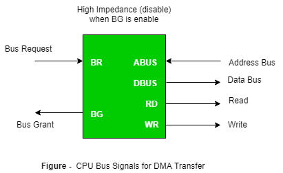
Fig 3 – CPU bus signals for DMA Transfer
Bus Request: It is used by the DMA controller to request the CPU to relinquish the control of the buses.
Bus Grant: It is activated by the CPU to Inform the external DMA controller that the buses are in a high impedance state and the requesting DMA can take control of the buses. Once the DMA has taken the control of the buses it transfers the data. This transfer can take place in many ways.
Types of DMA transfer using DMA controller:
Burst Transfer:
DMA returns the bus after the complete data transfer. A register is used as a byte count, being decremented for each byte transfer, and upon the byte count reaching zero, the DMAC will release the bus. When the DMAC operates in burst mode, the CPU is halted for the duration of the data transfer.
The steps involved are:
Bus grant request time.
Transfer the entire block of data at a transfer rate of the device because the device is usually slower than the speed at which the data can be transferred to the CPU.
Release the control of the bus back to the CPU
So, the total time is taken to transfer the N bytes
= Bus grant request time + (N) * (memory transfer rate) + Bus release control time.
Where,
X µsec =data transfer time or preparation time (words/block)
Y µsec =memory cycle time or cycle time or transfer time (words/block)
% CPU idle (Blocked)=(Y/X+Y)*100
% CPU Busy=(X/X+Y)*100
Cyclic Stealing:
An alternative method in which the DMA controller transfers one word at a time after which it must return the control of the buses to the CPU. The CPU delays its operation only for one memory cycle to allow the direct memory I/O transfer to “steal” one memory cycle.
Steps Involved are:
- Buffer the byte into the buffer
- Inform the CPU that the device has 1 byte to transfer (i.e. bus grant request)
- Transfer the byte (at system bus speed)
- Release the control of the bus back to the CPU.
Before moving on to transfer the next byte of data, the device performs step 1 again so that the bus isn’t tied up and the transfer won’t depend upon the transfer rate of the device.
So, for 1 byte of transfer of data, time is taken by using cycle stealing mode(T).
= time required for bus grant + 1 bus cycle to transfer data + time required to release the bus, it will be N x T
In cycle stealing mode we always follow pipelining concept that when one byte is getting transferred then the Device is parallel preparing the next byte. “The fraction of CPU time to the data transfer time” if asked then cycle stealing mode is used.
Where,
X µsec =data transfer time or preparation time
(words/block)
Y µsec =memory cycle time or cycle time or transfer
Time (words/block)
% CPU idle (Blocked) =(Y/X)*100
% CPU busy=(X/Y)*100
Interleaved mode: In this technique, the DMA controller takes over the system bus when the microprocessor is not using it. An alternate half-cycle i.e. half-cycle DMA + half-cycle processor.
Key takeaway
The method that is used to transfer information between internal storage and external I/O devices is known as the I/O interface. The CPU is interfaced using special communication links by the peripherals connected to any computer system. These communication links are used to resolve the differences between CPU and peripheral. There exist special hardware components between the CPU and peripherals to supervise and synchronize all the input and output transfers that are called interface units.
In Input-Output Transfer Techniques, the system requires the transfer of data between external circuitry and the microprocessor. In this section, we will discuss different ways of I/O transfer.
1. Program controlled I/O or Polling control.
2. Interrupt program-controlled I/O or interrupt-driven I/O.
3. Hardware controlled I/O.
4. I/O controlled by Handshake signals.
5. I/O controlled by a ready signal.
1. Program controlled I/O or Polling control:
In program-controlled I/O, the transfer of data is completely under the control of the microprocessor program. This means that the data transfer takes place only when Input-Output Transfer Techniques instructions are executed. In most cases, it is necessary to check whether the device is ready for data transfer or not. To check this, the microprocessor polls the status bit associated with the I/O device.
2. Interrupt program-controlled I/O or Interrupt driven I/O:
In the interrupt program-controlled approach, when a peripheral is ready to transfer data, it sends an interrupt signal to the microprocessor. This indicates that the Input-Output Transfer Techniques is initiated by the external I/O device. When interrupted, the microprocessor stops the execution of the program and transfers the program control to an interrupt service routine. This interrupt service routine performs the data transfer. After the data transfer, it returns control to the main program at the point it was interrupted.
3. Hardware controlled I/O:
To increase the speed of data transfer between memory and I/O, the hardware controlled I/O is used. It is commonly referred to as direct memory access (DMA). The hardware which controls this data transfer is commonly known as the DMA controller. The DMA controller sends a HOLD signal, to the microprocessor to initiate data transfer. In response to the HOLD signal microprocessor releases its data, address, and control buses to the DMA controller. Then the data transfer is controlled at high speed by the DMA controller without the intervention of the microprocessor. After data transfer, the DMA controller sends low on the HOLD pin, which gives them control of data, address, and control buses back to the microprocessor. This type of data transfer is used for large data transfers. This technique is explained in more detail in chapter 8.
4. I/O Control by handshake signals:
The handshake signals are used to ensure the readiness of the I/O device and to synchronize the timing of the data transfer. In this data transfer, the status of handshaking signals are checked between the microprocessor and an I/O device and when both are ready, the actual data is transferred.
5. I/O control by READY signal:
This technique is used to transfer data between the slower I/O device and the microprocessor. In some applications, the speed of the I/O system is not compatible with the microprocessor’s timings. This means that it takes a longer time to read/write data. In such situations, the microprocessor has to confirm whether a peripheral is ready to transfer data or not. If the READY pin is high, the peripheral is ready otherwise 8085 enters WAIT State or the WAIT States. These WAIT states elongate the read/write cycle timings and prepare 8085 microprocessor to communicate with slower I/O devices.
Key takeaway
In Input-Output Transfer Techniques, the system requires the transfer of data between external circuitry and the microprocessor. In this section, we will discuss different ways of I/O transfer.
1. Program controlled I/O or Polling control.
2. Interrupt program-controlled I/O or interrupt-driven I/O.
3. Hardware controlled I/O.
4. I/O controlled by Handshake signals.
5. I/O controlled by a ready signal.
Exceptions and interrupts are unexpected events that will disrupt the normal flow of execution of the instruction (that is currently executing by the processor). An exception is an unexpected event from within the processor. An interrupt is an unexpected event from outside the process.
Whenever an exception or interrupt occurs, the hardware starts executing the code that acts in response to the exception. This action may involve killing a process, outputting an error message, communicating with an external device, or crashing the entire computer system by initiating a “Blue Screen of Death” and halting the CPU. The instructions responsible for this action reside in the operating system kernel, and the code that performs this action is called the interrupt handler code. Now, We can think of handler code as an operating system subroutine. Then, After the handler code is executed, it may be possible to continue execution after the instruction where the execution or interrupt occurred.
Exception and Interrupt Handling:
Whenever an exception or interrupt occurs, execution transition from user mode to kernel mode where the exception or interrupt is handled. In detail, the following steps must be taken to handle an exception or interrupts.
While entering the kernel, the context (values of all CPU registers) of the currently executing process must first be saved to memory. The kernel is now ready to handle the exception/interrupt.
- Determine the cause of the exception/interrupt.
- Handle the exception/interrupt.
When the exception/interrupt have been handled the kernel performs the following steps:
- Select a process to restore and resume.
- Restore the context of the selected process.
- Resume execution of the selected process.
At any point in time, the values of all the registers in the CPU defines the context of the CPU. Another name used for CPU context is CPU state.
The exception/interrupt handler uses the same CPU as the currently executing process. When entering the exception/interrupt handler, the values in all CPU registers to be used by the exception/interrupt handler must be saved to memory. The saved register values can later be restored before resuming execution of the process.
The handler may have been invoked for several reasons. The handler thus needs to determine the cause of the exception or interrupt. Information about what caused the exception or interrupt can be stored in dedicated registers or at predefined addresses in memory.
Next, the exception or interrupt needs to be serviced. For instance, if it was a keyboard interrupt, then the key code of the keypress is obtained and stored somewhere or some other appropriate action is taken. If it was an arithmetic overflow exception, an error message may be printed or the program may be terminated.
The exception/interrupt has now been handled and the kernel. The kernel may choose to resume the same process that was executing before handling the exception/interrupt or resume execution of any other process currently in memory.
The context of the CPU can now be restored for the chosen process by reading and restoring all register values from memory.
The process selected to be resumed must be resumed at the same point it was stopped. The address of this instruction was saved by the machine when the interrupt occurred, so it is simply a matter of getting this address and make the CPU continue to execute at this address.
Key takeaway
Exceptions and interrupts are unexpected events that will disrupt the normal flow of execution of the instruction (that is currently executing by the processor). An exception is an unexpected event from within the processor. An interrupt is an unexpected event from outside the process.
Whenever an exception or interrupt occurs, the hardware starts executing the code that acts in response to the exception. This action may involve killing a process, outputting an error message, communicating with an external device, or crashing the entire computer system by initiating a “Blue Screen of Death” and halting the CPU. The instructions responsible for this action reside in the operating system kernel, and the code that performs this action is called the interrupt handler code. Now, We can think of handler code as an operating system subroutine. Then, After the handler code is executed, it may be possible to continue execution after the instruction where the execution or interrupt occurred.
Universal Serial Bus (USB)
Universal Serial Bus (USB) is an industry-standard that establishes specifications for connectors, cables, and protocols for communication, connection, and power supply between personal computers and their peripheral devices. There have been 3 generations of USB specifications:
1. USB 1.x
2. USB 2.0
3. USB 3.x
USB 2.0 has multiple updates and additions. The USB Implementer Forum (USB IF) currently maintains the USB standard and it was released in 1996.
USB was designed to standardize the connection of peripherals like pointing devices, keyboards, digital still and video cameras. But soon devices such as printers, portable media players, disk drives, and network adaptors to personal computers used USB to communicate and to supply electric power. It is commonplace to many devices and has largely replaced interfaces such as serial ports and parallel ports. USB connectors have replaced other types for battery chargers of portable devices with itself.
Advantages of USB –
The Universal Serial Bus was designed to simplify and improve the interface between personal computers and peripheral devices when compared with previously existing standard or ad-hoc proprietary interfaces.
- The USB interface is self-configuring. This means that the user need not adjust settings on the device and interface for speed or data format, or configure interrupts, input/output addresses, or direct memory access channels.
- USB connectors are standardized at the host, so any peripheral can use any available receptacle. USB takes full advantage of the additional processing power that can be economically put into peripheral devices so that they can manage themselves. USB devices mostly do not have user-adjustable interface settings.
- The USB interface is hot-pluggable or plugs and play, meaning devices can be exchanged without rebooting the host computer. Small devices can be powered directly from the USB interface thus removing extra power supply cables.
- The USB interface defines protocols for improving reliability over previous interfaces and recovery from common errors.
- Installation of a device relying on the USB standard minimal operator action is required.
Disadvantages of USB –
- USB cables are limited in length.
- USB has a strict “tree” topology and “master-slave” protocol for addressing peripheral devices. Peripheral devices cannot interact with one another except via the host, and two hosts cannot communicate over their USB ports directly.
- Some very high-speed peripheral devices require sustained speeds not available in the USB standard.
- For a product developer, the use of USB requires the implementation of a complex protocol and implies an intelligent controller in the peripheral device.
- The use of the USB logos on the product requires annual fees and membership in the organization.
Key takeaway
The interface between a computer’s hardware and its software is its architecture. The architecture is described by what the computer’s instructions do, and how they are specified. Understanding how it all works requires knowledge of the structure of a computer and its assembly language.
The computer is in a sense a communication system. Data is constantly being moved between the CPU, memory, and the various devices. The CPU uses I/O addresses to direct data to particular devices. The devices in turn use interrupt to notify the CPU and operating system of their needs.
Abstraction is one of the most important aspects of computing. It is a widely implemented Practice in the Computational field.
Memory Interleaving is less or More an Abstraction technique. Though it's a bit different from Abstraction. It is a Technique that divides memory into several modules such that Successive words in the address space are placed in the Different module.
Consecutive Word in a Module:
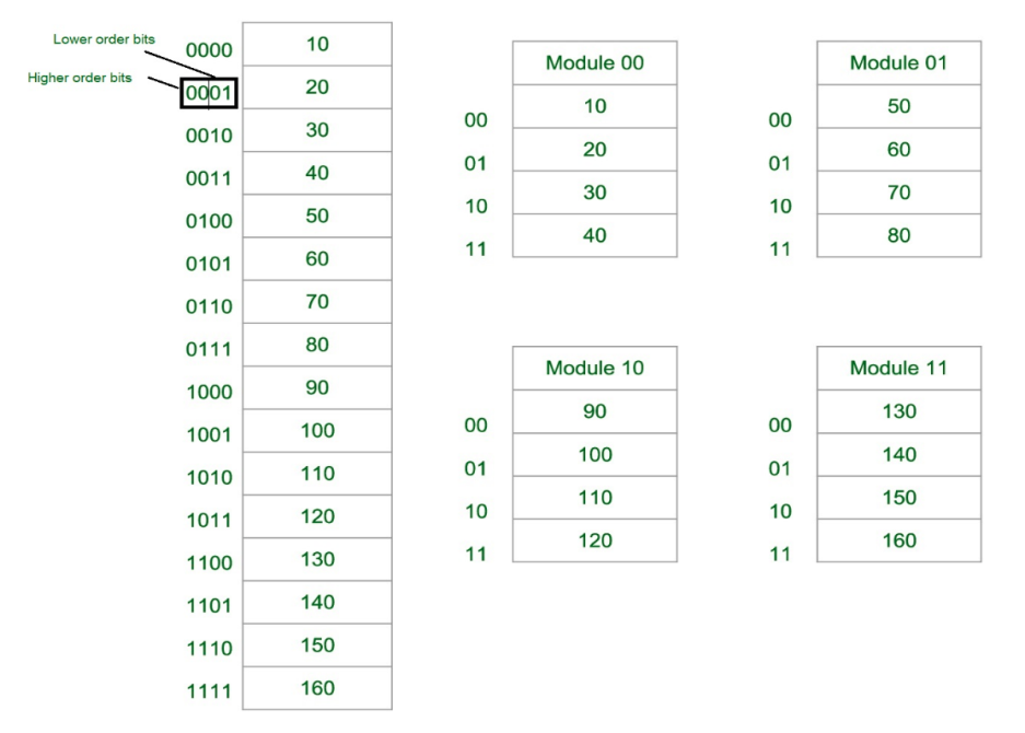
Fig-4: Consecutive Word in a Module
Let us assume 16 Data’s to be Transferred to the Four Module. Where Module 00 be Module 1, Module 01 be Module 2, Module 10 be Module 3 & Module 11 be Module 4. Also, 10, 20, 30….130 are the data to be transferred.
From the figure above in Module 1, 10 [Data] is transferred then 20, 30 & finally, 40 which are the Data. That means the data are added consecutively in the Module till its max capacity.
The most significant bit (MSB) provides the Address of the Module & the least significant bit (LSB) provides the address of the data in the module.
For Example, to get 90 (Data) 1000 will be provided by the processor. This 10 will indicate that the data is in module 10 (module 3) & 00 is the address of 90 in Module 10 (module 3). So,
Module 1 Contains Data : 10, 20, 30, 40
Module 2 Contains Data : 50, 60, 70, 80
Module 3 Contains Data : 90, 100, 110, 120
Module 4 Contains Data : 130, 140, 150, 160
Consecutive Word in Consecutive Module:
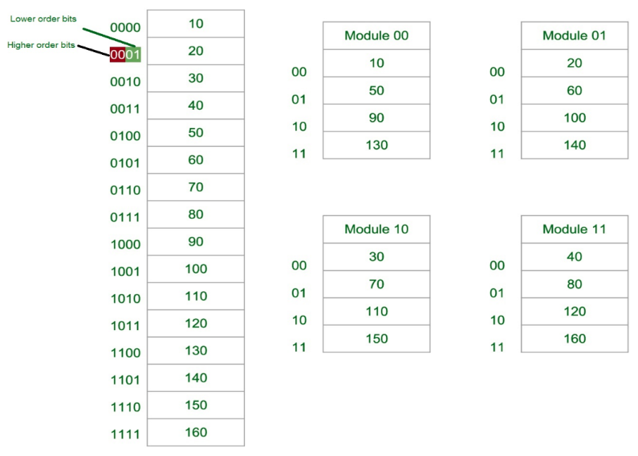
Fig-5: Consecutive Word in Consecutive Module
Now again we assume 16 Data’s to be transferred to the Four Module. But Now the consecutive Data are added in the Consecutive Module. That is, 10 [Data] is added in Module 1, 20 [Data] in Module 2 and So on.
The Least Significant Bit (LSB) provides the Address of the Module & the Most significant bit (MSB) provides the address of the data in the module.
For Example, to get 90 (Data) 1000 will be provided by the processor. This 00 will indicate that the data is in module 00 (module 1) & 10 is the address of 90 in Module 00 (module 1). That is,
Module 1 Contains Data : 10, 50, 90, 130
Module 2 Contains Data : 20, 60, 100, 140
Module 3 Contains Data : 30, 70, 110, 150
Module 4 Contains Data : 40, 80, 120, 160
Why we use Memory Interleaving? [Advantages]:
Whenever Processor requests Data from the main memory. A block (chunk) of Data is Transferred to the cache and then to Processor. So whenever a cache miss occurs the Data is to be fetched from the main memory. But main memory is relatively slower than the cache. So to improve the access time of the main memory interleaving is used.
We can access all four Modules at the same time thus achieving Parallelism. From Figure 2 the data can be acquired from the Module using the Higher bits. This method Uses memory effectively.
Types of Memory Interleaving
Memory Interleaving is an abstraction technique that divides memory into some modules such that successive words in the address space are placed in the different modules.
Suppose a 64 MB memory made up of the 4 MB chips as shown in the below:
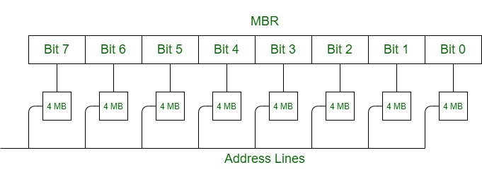
Fig 6 – Example
We organize the memory into 4 MB banks, each having eight of the 4 MB chips. The memory thus has 16 banks, each of 4 MB.
64 MB memory = 2^26, so 26 bits are used for addressing.
16 = 2^4, so 4 bits of the address select the bank, and 4 MB = 2^22, so 22 bits of the address to each chip.
In general, an N-bit address, with N = L + M, is broken into two parts:
- L-bit bank select used to activate one of the 2^L banks of memory, and
- M-bit address that is sent to each of the memory banks.
When one of the memory banks is active, the other (2L – 1) are inactive. All banks receive the M-bit address, but the inactive ones do not respond to it.
Classification of Memory Interleaving:
Memory interleaving is classified into two types:
1. High Order Interleaving –
In high-order interleaving, the most significant bits of the address select the memory chip. The least significant bits are sent as addresses to each chip. One problem is that consecutive addresses tend to be in the same chip. The maximum rate of data transfer is limited by the memory cycle time.
It is also known as Memory Banking.
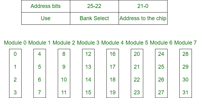
Fig 7 – Memory banking
2. Low Order Interleaving –
In low-order interleaving, the least significant bits select the memory bank (module). In this, consecutive memory addresses are in different memory modules. This allows memory access at much faster rates than allowed by the cycle time.
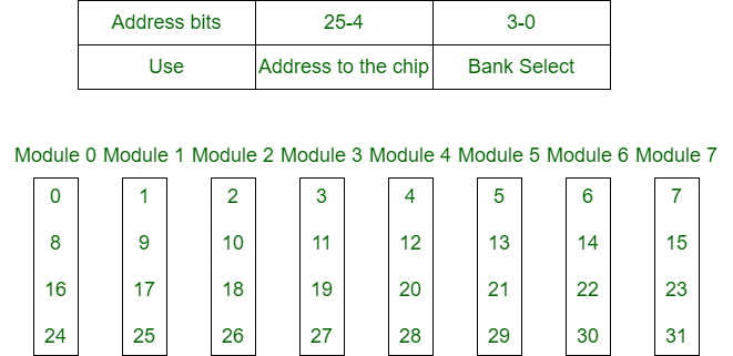
Fig 8 – Low order interleaving memory bank
Key takeaway
Abstraction is one of the most important aspects of computing. It is a widely implemented Practice in the Computational field.
Memory Interleaving is less or More an Abstraction technique. Though it's a bit different from Abstraction. It is a Technique that divides memory into several modules such that Successive words in the address space are placed in the Different module.
A memory unit is an essential component in any digital computer since it is needed for storing programs and data.
Typically, a memory unit can be classified into two categories:
- The memory unit that establishes direct communication with the CPU is called Main Memory. The main memory is often referred to as RAM (Random Access Memory).
- The memory units that provide backup storage are called Auxiliary Memory. For instance, magnetic disks and magnetic tapes are the most commonly used auxiliary memories.
Apart from the basic classifications of a memory unit, the memory hierarchy consists of all of the storage devices available in a computer system ranging from the slow but high-capacity auxiliary memory to relatively faster main memory.
The following image illustrates the components in a typical memory hierarchy.
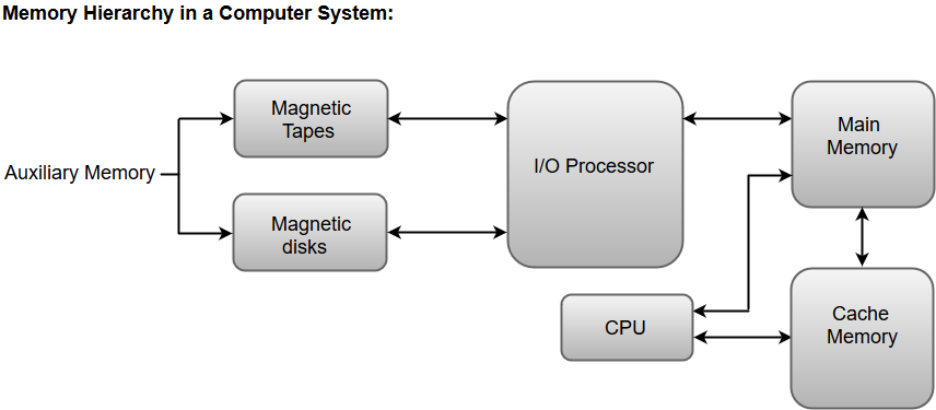
Fig 9 – Memory hierarchy in a computer system
Auxiliary Memory
Auxiliary memory is known as the lowest-cost, highest-capacity, and slowest-access storage in a computer system. Auxiliary memory provides storage for programs and data that are kept for long-term storage or when not in immediate use. The most common examples of auxiliary memories are magnetic tapes and magnetic disks.
A magnetic disk is a digital computer memory that uses a magnetization process to write, rewrite and access data. For example, hard drives, zip disks, and floppy disks.
Magnetic tape is a storage medium that allows for data archiving, collection, and backup for different kinds of data.
Main Memory
The main memory in a computer system is often referred to as Random Access Memory (RAM). This memory unit communicates directly with the CPU and with auxiliary memory devices through an I/O processor.
The programs that are not currently required in the main memory are transferred into auxiliary memory to provide space for currently used programs and data.
I/O Processor
The primary function of an I/O Processor is to manage the data transfers between auxiliary memories and the main memory.
Cache Memory
The data or contents of the main memory that are used frequently by the CPU are stored in the cache memory so that the processor can easily access that data in a shorter time. Whenever the CPU requires accessing memory, it first checks the required data into the cache memory. If the data is found in the cache memory, it is read from the fast memory. Otherwise, the CPU moves onto the main memory for the required data.
Key takeaway
A memory unit is an essential component in any digital computer since it is needed for storing programs and data.
Typically, a memory unit can be classified into two categories:
- The memory unit that establishes direct communication with the CPU is called Main Memory. The main memory is often referred to as RAM (Random Access Memory).
- The memory units that provide backup storage are called Auxiliary Memory. For instance, magnetic disks and magnetic tapes are the most commonly used auxiliary memories.
Cache Memory
The data or contents of the main memory that are used frequently by the CPU are stored in the cache memory so that the processor can easily access that data in a shorter time. Whenever the CPU needs to access memory, it first checks the cache memory. If the data is not found in the cache memory, then the CPU moves into the main memory.
Cache memory is placed between the CPU and the main memory. The block diagram for a cache memory can be represented as:

Fig 10 – Cache memory
The cache is the fastest component in the memory hierarchy and approaches the speed of CPU components.
The basic operation of cache memory is as follows:
- When the CPU needs to access memory, the cache is examined. If the word is found in the cache, it is read from the fast memory.
- If the word addressed by the CPU is not found in the cache, the main memory is accessed to read the word.
- A block of words one just accessed is then transferred from main memory to cache memory. The block size may vary from one word (the one just accessed) to about 16 words adjacent to the one just accessed.
- The performance of the cache memory is frequently measured in terms of a quantity called hit ratio.
- When the CPU refers to memory and finds the word in the cache, it is said to produce a hit.
- If the word is not found in the cache, it is in the main memory and it counts as a miss.
- The ratio of the number of hits divided by the total CPU references to memory (hits plus misses) is the hit ratio.
Cache Memory is a special very high-speed memory. It is used to speed up and synchronizing with a high-speed CPU. Cache memory is costlier than main memory or disk memory but economical than CPU registers. Cache memory is an extremely fast memory type that acts as a buffer between RAM and the CPU. It holds frequently requested data and instructions so that they are immediately available to the CPU when needed.
Cache memory is used to reduce the average time to access data from the Main memory. The cache is a smaller and faster memory that stores copies of the data from frequently used main memory locations. There are various independent caches in a CPU, which store instructions and data.

Fig 11 – Memory
Levels of memory:
- Level 1 or Register –
It is a type of memory in which data is stored and accepted that are immediately stored in the CPU. The most commonly used register is accumulator, Program counter, address register, etc.
- Level 2 or Cache memory –
It is the fastest memory which has faster access time where data is temporarily stored for faster access.
- Level 3 or Main Memory –
It is the memory on which the computer works currently. It is small in size and once power is off data no longer stays in this memory.
- Level 4 or Secondary Memory –
It is external memory that is not as fast as main memory but data stays permanently in this memory.
Cache Performance:
When the processor needs to read or write a location in the main memory, it first checks for a corresponding entry in the cache.
- If the processor finds that the memory location is in the cache, a cache hit has occurred and data is read from the cache
- If the processor does not find the memory location in the cache, a cache miss has occurred. For a cache miss, the cache allocates a new entry and copies in data from the main memory, then the request is fulfilled from the contents of the cache.
The performance of cache memory is frequently measured in terms of a quantity called the Hit ratio.
Hit ratio = hit / (hit + miss) = no. Of hits/total accesses
We can improve Cache performance using higher cache block size, higher associativity, reduce miss rate, reduce miss penalty, and reduce the time to hit in the cache.
Cache Mapping:
There are three different types of mapping used for cache memory which are as follows: Direct mapping, Associative mapping, and Set-Associative mapping. These are explained below.
- Direct Mapping –
The simplest technique, known as direct mapping, maps each block of main memory into only one possible cache line. Or
In Direct mapping, assign each memory block to a specific line in the cache. If a line is previously taken up by a memory block when a new block needs to be loaded, the old block is trashed. An address space is split into two parts index field and a tag field. The cache is used to store the tag field whereas the rest is stored in the main memory. Direct mappings performance is directly proportional to the Hit ratio.
2. i = j modulo m
3. where
4. i=cache line number
5. j= main memory block number
m=number of lines in the cache
For purposes of cache access, each main memory address can be viewed as consisting of three fields. The least significant w bits identify a unique word or byte within a block of main memory. In most contemporary machines, the address is at the byte level. The remaining s bits specify one of the 2s blocks of main memory. The cache logic interprets these s bits as a tag of s-r bits (most significant portion) and a line field of r bits. This latter field identifies one of the m=2r lines of the cache.

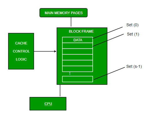
Fig 12 – Direct mapping
2. Associative Mapping –
In this type of mapping, the associative memory is used to store content and addresses of the memory word. Any block can go into any line of the cache. This means that the word id bits are used to identify which word in the block is needed, but the tag becomes all of the remaining bits. This enables the placement of any word at any place in the cache memory. It is considered to be the fastest and the most flexible mapping form.
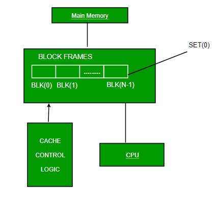
Fig 13 – Associative mapping
3. Set-associative Mapping –
This form of mapping is an enhanced form of direct mapping where the drawbacks of direct mapping are removed. Set associative addresses the problem of possible thrashing in the direct mapping method. It does this by saying that instead of having exactly one line that a block can map to in the cache, we will group a few lines creating a set. Then a block in memory can map to any one of the lines of a specific set. Set-associative mapping allows that each word that is present in the cache can have two or more words in the main memory for the same index address. Set associative cache mapping combines the best of direct and associative cache mapping techniques.
In this case, the cache consists of several sets, each of which consists of several lines. The relationships are
m = v * k
i= j mod v
Where
i=cache set number
j=main memory block number
v=number of sets
m=number of lines in the cache number of sets
k=number of lines in each set

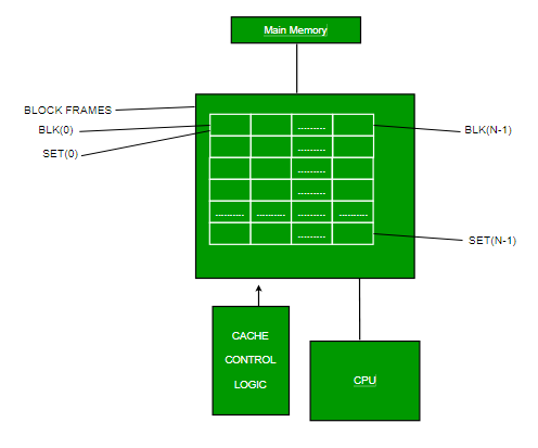
Fig 14 – Set associative mapping
Application of Cache Memory –
- Usually, the cache memory can store a reasonable number of blocks at any given time, but this number is small compared to the total number of blocks in the main memory.
- The correspondence between the main memory blocks and those in the cache is specified by a mapping function.
Types of Cache –
- Primary Cache –
A primary cache is always located on the processor chip. This cache is small and its access time is comparable to that of processor registers.
2. Secondary Cache –
Secondary cache is placed between the primary cache and the rest of the memory. It is referred to as the level 2 (L2) cache. Often, the Level 2 cache is also housed on the processor chip.
Locality of reference –
Since size of cache memory is less as compared to main memory. So to check which part of main memory should be given priority and loaded in cache is decided based on locality of reference.
Types of Locality of reference
- Spatial Locality of reference
This says that there is a chance that the element will be present in the proximity to the reference point and next time if again searched then more proximity to the point of reference.
2. Temporal Locality of reference
This Least recently used algorithm will be used. Whenever there is page fault occurs within a word will not only load word in the main memory but complete page fault will be loaded because the spatial locality of reference rule says that if you are referring to any word next word will be referred to in its register that’s why we load complete page table so the complete block will be loaded.
Key takeaway
The data or contents of the main memory that are used frequently by the CPU are stored in the cache memory so that the processor can easily access that data in a shorter time. Whenever the CPU needs to access memory, it first checks the cache memory. If the data is not found in the cache memory, then the CPU moves into the main memory.
Cache memory bridges the speed mismatch between the processor and the main memory.
When a cache hit occurs,
- The required word is present in the cache memory.
- The required word is delivered to the CPU from the cache memory.
When a cache miss occurs,
- The required word is not present in the cache memory.
- The page containing the required word has to be mapped from the main memory.
- This mapping is performed using cache mapping techniques.
In this article, we will discuss different cache mapping techniques.
Cache Mapping-
- Cache mapping defines how a block from the main memory is mapped to the cache memory in case of a cache miss.
OR
- Cache mapping is a technique by which the contents of the main memory are brought into the cache memory.
The following diagram illustrates the mapping process-
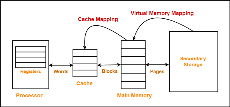
Fig 15 – Mapping process
Now, before proceeding further, it is important to note the following points-
NOTES
- Main memory is divided into equal size partitions called blocks or frames.
- Cache memory is divided into partitions having the same size as blocks called lines.
- During cache mapping, a block of main memory is simply copied to the cache, and the block is not brought from the main memory.
Cache Mapping Techniques-
Cache mapping is performed using the following three different techniques-

- Direct Mapping
- Fully Associative Mapping
- K-way Set Associative Mapping
1. Direct Mapping-
In direct mapping,
- A particular block of main memory can map only to a particular line of the cache.
- The line number of cache to which a particular block can map is given by-
Cache line number
= ( Main Memory Block Address ) Modulo (Number of lines in Cache)
Example-
- Consider cache memory is divided into ‘n’ number of lines.
- Then, block ‘j’ of main memory can map to line number (j mod n) only of the cache.
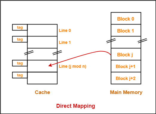
Fig 16 – Direct mapping
The need for a Replacement Algorithm-
In direct mapping,
- There is no need for any replacement algorithm.
- This is because the main memory block can map only to a particular line of the cache.
- Thus, the new incoming block will always replace the existing block (if any) in that particular line.
Division of Physical Address-
In direct mapping, the physical address is divided as-
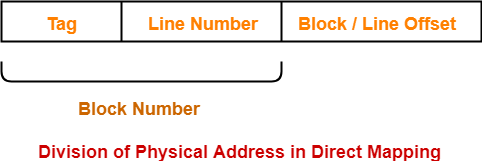
Fig 17 – Physical address
2. Fully Associative Mapping-
In fully associative mapping,
- A block of main memory can map to any line of the cache that is freely available at that moment.
- This makes fully associative mapping more flexible than direct mapping.
Example-
Consider the following scenario-
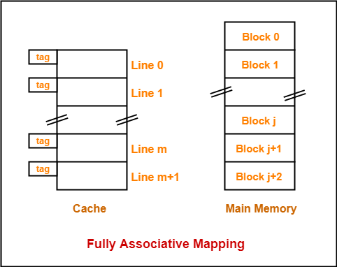
Fig 18 – Fully associative mapping
Here,
- All the lines of cache are freely available.
- Thus, any block of main memory can map to any line of the cache.
- Had all the cache lines been occupied, then one of the existing blocks will have to be replaced.
The need for a Replacement Algorithm-
In fully associative mapping,
- A replacement algorithm is required.
- The replacement algorithm suggests the block be replaced if all the cache lines are occupied.
- Thus, replacement algorithm like FCFS Algorithm, LRU Algorithm, etc is employed.
Division of Physical Address-
In fully associative mapping, the physical address is divided as-

Fig 19 – Physical address
3. K-way Set Associative Mapping-
In k-way set associative mapping,
- Cache lines are grouped into sets where each set contains a k number of lines.
- A particular block of main memory can map to only one particular set of the cache.
- However, within that set, the memory block can map any freely available cache line.
- The set of the cache to which a particular block of the main memory can map is given by-
Cache set number
= ( Main Memory Block Address ) Modulo (Number of sets in Cache)
Example-
Consider the following example of 2-way set associative mapping-
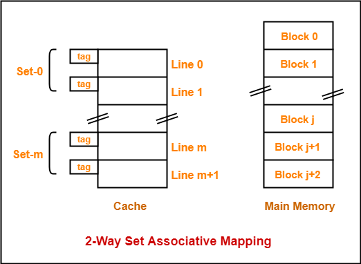
Fig 20 – 2-way set associative mapping
Here,
- k = 2 suggests that each set contains two cache lines.
- Since cache contains 6 lines, so number of sets in the cache = 6 / 2 = 3 sets.
- Block ‘j’ of main memory can map to set number (j mod 3) only of the cache.
- Within that set, block ‘j’ can map to any cache line that is freely available at that moment.
- If all the cache lines are occupied, then one of the existing blocks will have to be replaced.
The need for a Replacement Algorithm-
- Set associative mapping is a combination of direct mapping and fully associative mapping.
- It uses fully associative mapping within each set.
- Thus, set-associative mapping requires a replacement algorithm.
Division of Physical Address-
In set associative mapping, the physical address is divided as-

Fig 21 – Physical address
Special Cases-
- If k = 1, then k-way set associative mapping becomes direct mapping i.e.
1-way Set Associative Mapping ≡ Direct Mapping
- If k = Total number of lines in the cache, then k-way set associative mapping becomes fully associative mapping.
Key takeaway
Cache Mapping-
- Cache mapping defines how a block from the main memory is mapped to the cache memory in case of a cache miss.
OR
- Cache mapping is a technique by which the contents of the main memory are brought into the cache memory.
In an operating system that uses paging for memory management, a page replacement algorithm is needed to decide which page needs to be replaced when a new page comes in.
Page Fault – A page fault happens when a running program accesses a memory page that is mapped into the virtual address space but not loaded in physical memory.
Since actual physical memory is much smaller than virtual memory, page faults happen. In case of a page fault, Operating System might have to replace one of the existing pages with the newly needed page. Different page replacement algorithms suggest different ways to decide which page to replace. The target for all algorithms is to reduce the number of page faults.
Page Replacement Algorithms:
- First In First Out (FIFO) –
This is the simplest page replacement algorithm. In this algorithm, the operating system keeps track of all pages in the memory in a queue, the oldest page is in the front of the queue. When a page needs to be replaced page in the front of the queue is selected for removal.
Example-1 Consider page reference string 1, 3, 0, 3, 5, 6 with 3 page frames. Find several page faults.
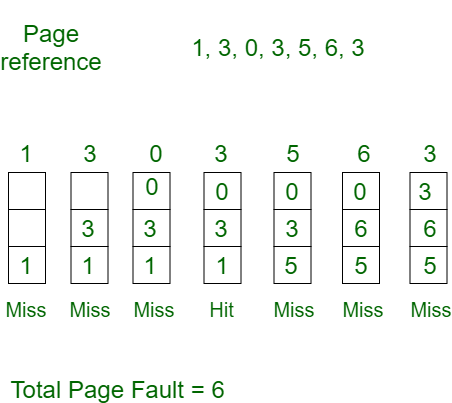
Initially, all slots are empty, so when 1, 3, 0 came they are allocated to the empty slots —> 3 Page Faults.
When 3 comes, it is already in memory so —> 0 Page Faults.
Then 5 comes, it is not available in memory so it replaces the oldest page slot i.e 1. —>1 Page Fault.
6 comes, it is also not available in memory so it replaces the oldest page slot i.e 3 —>1 Page Fault.
Finally, when 3 come it is not available so it replaces 0 1 page fault
Belady’s anomaly – Belady’s anomaly proves that it is possible to have more page faults when increasing the number of page frames while using the First in First Out (FIFO) page replacement algorithm. For example, if we consider reference string 3, 2, 1, 0, 3, 2, 4, 3, 2, 1, 0, 4, and 3 slots, we get 9 total page faults, but if we increase slots to 4, we get 10-page faults.
- Optimal Page replacement –
In this algorithm, pages are replaced which would not be used for the longest duration of time in the future.
Example-2: Consider the page references 7, 0, 1, 2, 0, 3, 0, 4, 2, 3, 0, 3, 2, with 4 page frame. Find number of page fault.
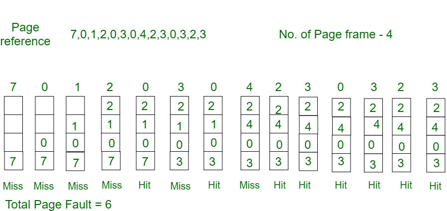
Initially, all slots are empty, so when 7 0 1 2 are allocated to the empty slots —> 4 Page faults
0 is already there so —> 0 Page fault.
When 3 came it will take the place of 7 because it is not used for the longest duration of time in the future.—>1 Page fault.
0 is already there so —> 0 Page fault.
4 will takes place of 1 —> 1 Page Fault.
Now for the further page reference string —> 0 Page fault because they are already available in the memory.
Optimal page replacement is perfect, but not possible in practice as the operating system cannot know future requests. The use of Optimal Page replacement is to set up a benchmark so that other replacement algorithms can be analyzed against it.
- Least Recently Used –
In this algorithm, the page will be replaced which is the least recently used.
Example-3: Consider the page reference string 7, 0, 1, 2, 0, 3, 0, 4, 2, 3, 0, 3, 2 with 4 page frames. Find number of page faults.
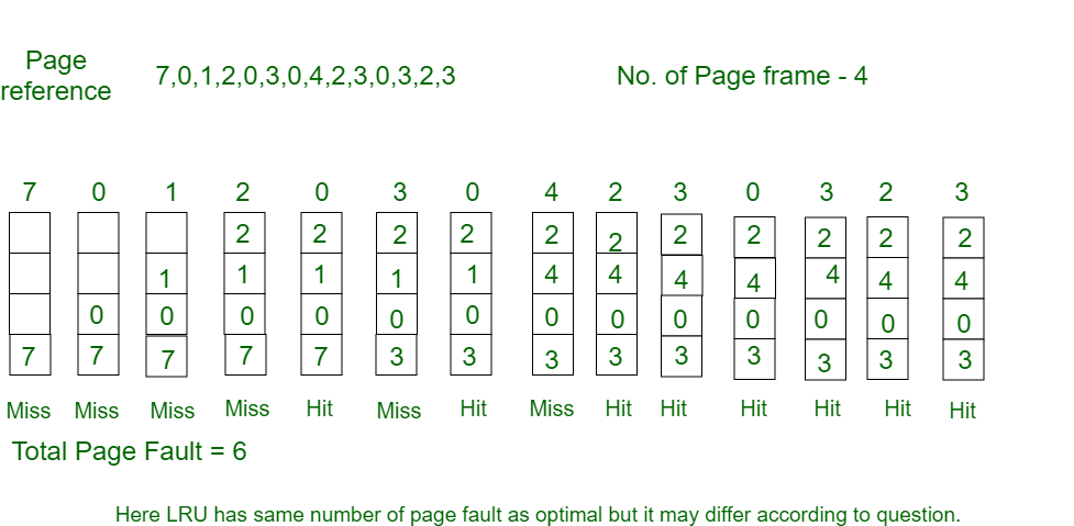
Initially, all slots are empty, so when 7 0 1 2 are allocated to the empty slots —> 4 Page faults
0 is already their so —> 0 Page fault.
When 3 came it will take the place of 7 because it is least recently used —>1 Page fault
0 is already in memory so —> 0 Page fault.
4 will takes place of 1 —> 1 Page Fault
Now for the further page reference string —> 0 Page fault because they are already available in the memory.
Key takeaway
A page fault happens when a running program accesses a memory page that is mapped into the virtual address space but not loaded in physical memory.
Since actual physical memory is much smaller than virtual memory, page faults happen. In case of a page fault, Operating System might have to replace one of the existing pages with the newly needed page. Different page replacement algorithms suggest different ways to decide which page to replace. The target for all algorithms is to reduce the number of page faults.
Normally we can perform both read operation and write operation on the cache memory.
Now when we perform a read operation on cache memory then it does not change the content of the memory. But as it is obvious that any write operation performed on the cache changes the content of the memory. Thus it is important to perform any write on cache very carefully.
To make sure write operation is performed carefully, we can adopt two cache write methods:
- Write-through policy
- Write-back policy
Let's learn about the above two cache write methods in computer architecture.
Write-through policy
The write-through policy is the most commonly used methods of writing into the cache memory.
In the write-through method when the cache memory is updated simultaneously the main memory is also updated. Thus at any given time, the main memory contains the same data which is available in the cache memory.
It is to be noted that, the write-through technique is a slow process as every time it needs to access the main memory.
Write-back policy
The write-back policy can also be used for cache writing.
During a write operation, only the cache location is updated while following the write-back method. When an update in cache occurs then the updated location is marked by a flag. The flag is known as modified or dirty bit.
When the word is replaced from the cache, it is written into the main memory if its flag bit is set. The logic behind this technique is based on the fact that during a cache write operation, the word present in the cache may be accessed several times (temporal locality of reference). This method helps reduce the number of references to the main memory.
The only limitation to the write-back technique is that inconsistency may occur while adopting this technique due to two different copies of the same data, one in the cache and the other in main memory.
Key takeaway
The write-through policy is the most commonly used methods of writing into the cache memory.
In the write-through method when the cache memory is updated simultaneously the main memory is also updated. Thus at any given time, the main memory contains the same data which is available in the cache memory.
The write-back policy can also be used for cache writing.
During a write operation, only the cache location is updated while following the write-back method. When an update in cache occurs then the updated location is marked by a flag. The flag is known as modified or dirty bit.
References:
1. “Computer Organization and Design: The Hardware/Software Interface”, 5th Edition by David A. Patterson and John L. Hennessy, Elsevier.
2. “Computer Organization and Embedded Systems”, 6th Edition by Carl Hamacher, McGraw Hill Higher Education.
3. “Computer Architecture and Organization”, 3rd Edition by John P. Hayes, WCB/McGraw-Hill
4. “Computer Organization and Architecture: Designing for Performance”, 10th Edition by William Stallings, Pearson Education.
5. “Computer System Design and Architecture”, 2nd Edition by Vincent P. Heuring and Harry F. Jordan, Pearson Education.