Unit - 2
Combinational Circuits
- It works as an inverse of an encoder.
- It is a combinational circuit which converts n input lines into 2n output lines.
- Taking an example of 3-to-8 line decoder.
Truth Table –
X | Y | Z | D0 | D1 | D2 | D3 | D4 | D5 | D6 | D7 |
0 | 0 | 0 | 1 | 0 | 0 | 0 | 0 | 0 | 0 | 0 |
0 | 0 | 1 | 0 | 1 | 0 | 0 | 0 | 0 | 0 | 0 |
0 | 1 | 0 | 0 | 0 | 1 | 0 | 0 | 0 | 0 | 0 |
0 | 1 | 1 | 0 | 0 | 0 | 1 | 0 | 0 | 0 | 0 |
1 | 0 | 0 | 0 | 0 | 0 | 0 | 1 | 0 | 0 | 0 |
1 | 0 | 1 | 0 | 0 | 0 | 0 | 0 | 1 | 0 | 0 |
1 | 1 | 0 | 0 | 0 | 0 | 0 | 0 | 0 | 1 | 0 |
1 | 1 | 1 | 0 | 0 | 0 | 0 | 0 | 0 | 0 | 1 |
Implementation
D0 is high when X = 0, Y = 0 and Z = 0. Hence,
D0 = X’ Y’ Z’
Similarly,
D1 = X’ Y’ Z
D2 = X’ Y Z’
D3 = X’ Y Z
D4 = X Y’ Z’
D5 = X Y’ Z
D6 = X Y Z’
D7 = X Y Z
Hence,
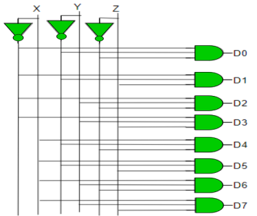
Fig. Decoder
Key Takeaways:
- It works as an inverse of an encoder.
- It is a combinational circuit which converts n input lines into 2n output lines.
- Binary code of N digits is used to store 2N distinct elements of coded information.
- This is the reason why encoders and decoders are used.
- Encoders convert 2N lines of input into a code of N bits and Decoders decode those N bits into 2N lines.
Encoders –
- It is a combinational circuit that converts binary information in the form of a 2N input lines into N output lines, which represent N bit code for the input.
- For simple encoders, only one input line is active at a time.
- For example: Octal to Binary encoder takes 8 input lines and generates 3 output lines.
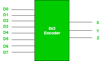
Fig.: 8X3 Encoder
Truth Table –
D7 | D6 | D5 | D4 | D3 | D2 | D1 | D0 | X | Y | Z |
0 | 0 | 0 | 0 | 0 | 0 | 0 | 1 | 0 | 0 | 0 |
0 | 0 | 0 | 0 | 0 | 0 | 1 | 0 | 0 | 0 | 1 |
0 | 0 | 0 | 0 | 0 | 1 | 0 | 0 | 0 | 1 | 0 |
0 | 0 | 0 | 0 | 1 | 0 | 0 | 0 | 0 | 1 | 1 |
0 | 0 | 0 | 1 | 0 | 0 | 0 | 0 | 1 | 0 | 0 |
0 | 0 | 1 | 0 | 0 | 0 | 0 | 0 | 1 | 0 | 1 |
0 | 1 | 0 | 0 | 0 | 0 | 0 | 0 | 1 | 1 | 0 |
1 | 0 | 0 | 0 | 0 | 0 | 0 | 0 | 1 | 1 | 1 |
- From the above truth table, it is seen that the output is 000 when D0 is active; 001 when D1 is active; 010 when D2 is active and so on.
Implementation –
- From the above truth table, the output Z is active when the input octal digit is 1, 3, 5 or 7.
- Y is active when input octal digit is 2, 3, 6 or 7 and X is active when input octal digits 4, 5, 6 or 7.
- Hence, the Boolean functions would be:
X = D4 + D5 + D6 + D7
Y = D2 +D3 + D6 + D7
Z = D1 + D3 + D5 + D7
- Hence, the encoder is realized with OR gates as follows:
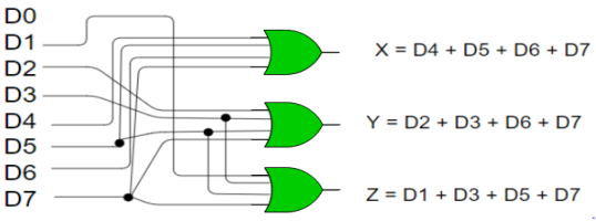
Fig: 8:3 encoder
- Limitation of the encoder is that only one input is active at a time.
- If more than one input is active, then the output of encoder is undefined.
- For example, if D6 and D3 are both active, then, our output would be 111 which is the output for D7.
- Problem arises when all inputs are 0.
- The encoder gives output 000 which actually is the output for D0. To avoid this, an extra bit is added to the output which is called the valid bit whose value is 0 when all inputs are 0 or 1.
- It is an encoder whose inputs are given priorities.
- When more than one input becomes active at the same time then the input with higher priority takes precedence w.r.to the output which is generated.
- Considering a 4:2 priority encoder.
- From the truth table given below we see that when all inputs are 0, V bit is zero and outputs are not used.
- The x in the table shows the don’t care condition, i.e. it can be 0 or 1.
- Here, D3 has highest priority, therefore, when D3 is high, output has to be 11.
- D0 has the lowest priority, hence the output would be 00 only when D0 is high and all the other input lines are low.
Truth Table –
D3 | D2 | D1 | D0 | X | Y | V |
0 | 0 | 0 | 0 | x | x | 0 |
0 | 0 | 0 | 1 | 0 | 0 | 1 |
0 | 0 | 1 | x | 0 | 1 | 1 |
0 | 1 | X | x | 1 | 0 | 1 |
1 | x | X | x | 1 | 1 | 1 |
Implementation
The condition for valid bit to be 1 is when at least one of the inputs should be high. Hence,
V = D0 + D1 + D2 + D3
For X:
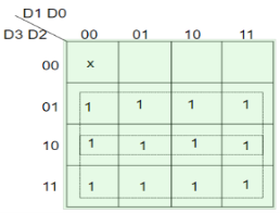
=>X=D2+D3
For Y:
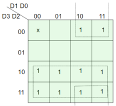
=> Y = D1 D2’ + D3
Hence, the priority 4-to-2 encoder can be realized as follows:
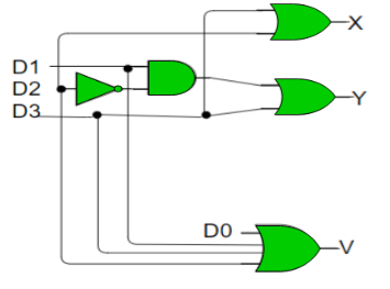
Fig: Priority encoder
Key takeaway
An Encoder is a combinational circuit that performs the reverse operation of Decoder. It has maximum of 2n input lines and ‘n’ output lines. It will produce a binary code equivalent to the input, which is active High.
- It is a special type of combinational circuit.
- It has n-data inputs, one output and m inputs select lines with 2m = n.
- It selects one of the n data inputs and routes it to the output.
- The selection of one of the inputs is done by the select lines.
- Depending on the code applied at the inputs, one of the n data sources is selected and transmitted to the single output Y.
- E is the enable input which is useful for cascading purpose.
- It is an active low terminal hence performs the required operation when it is low.
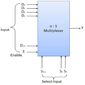
Fig. Block diagram of multiplexer
Multiplexers come in multiple variations
- 2: 1 multiplexer
- 4: 1 multiplexer
- 16: 1 multiplexer
- 32: 1 multiplexer
Block Diagram of 2:1 MUX
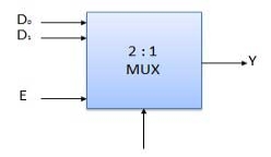
Truth Table of 2:1 MUX
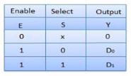
Where x is don’t care.
Key Takeaways
- It has n-data inputs, one output and m inputs select lines with 2m = n.
- The selection of one of the inputs is done by the select lines.
- It performs the inverse operation of a multiplexer as it receives one input and distributes it across its outputs.
- It has only one input and n outputs with m select input.
- At a time only one output line is selected by the select lines and that input is transmitted through the output line.
- It is equivalent to a single pole multiple way switch.
Various Demultiplexers are used as:
- 1: 2 demultiplexer
- 1: 4 demultiplexer
- 1: 16 demultiplexer
- 1: 32 demultiplexer
Block diagram
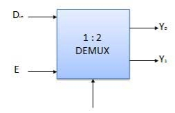
Truth Table
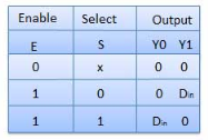
Where x is don’t care.
Key Takeaways:
- It performs the inverse operation of a multiplexer as it receives one input and distributes it across its outputs.
- It has only one input and n outputs with m select input.
Binary To Gray Code
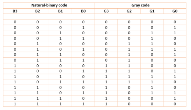
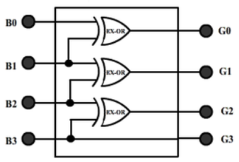
For this circuit, B3 B2 B1 B0 are inputs while G3 G2 G1 G0 are outputs.
K-map for the outputs:
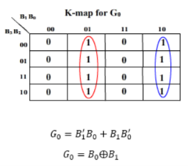
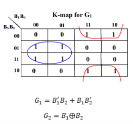
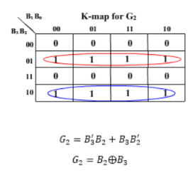
And G3 = B3
Gray To Binary Code
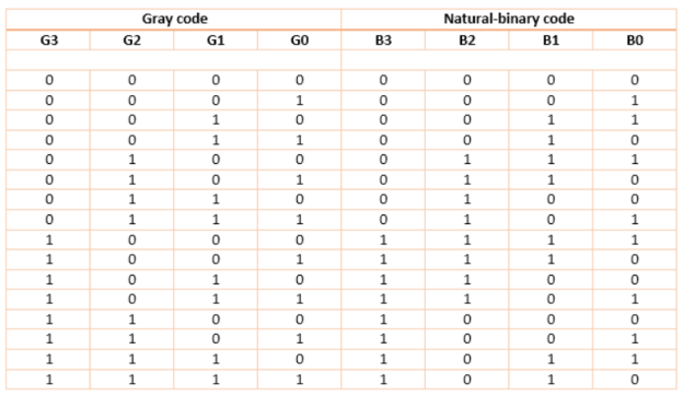
Then the K-maps:
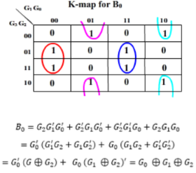
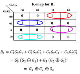
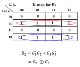
And B3 = G3
The realization of Gray-to-Binary converter is
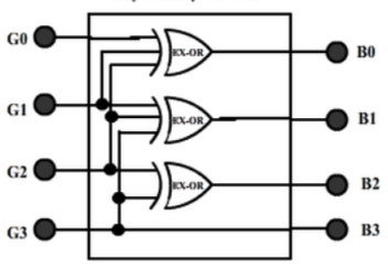
Key Takeaways:
- These are the combinational circuits made by conversion of one code to another.
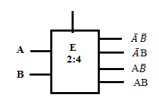
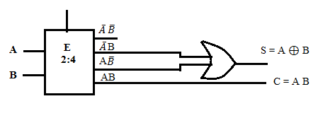
Half adder using decoder
S = A ⊕ B = 
C = AB
Half Subtractor
D = A ⊕ B
Borrow = 

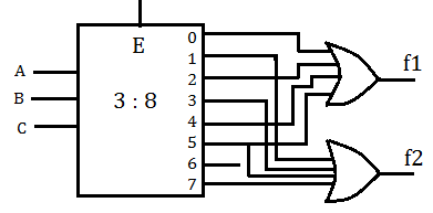
f1 = ∑m (0,2,4,5)
f2 = ∑m (1,3,5,6,7)
Half Adder
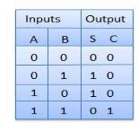
It is a combinational circuit which has two inputs and two outputs.
It is designed to add two single bit binary number A and B.
It has two outputs carry and sum.
Block diagram
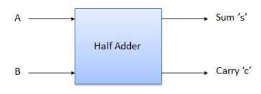
Fig. Half adder
Truth Table
Circuit Diagram
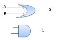
Fig. Half adder
Full Adder
- It is developed to overcome the drawback of Half Adder circuit.
- It can add two one-bit numbers A and B and a carry C.
- It is a three input and two output combinational circuit.
Block diagram
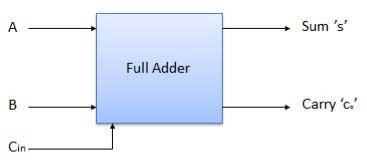
Fig. Full adder
Truth Table
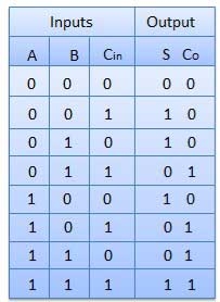
Circuit Diagram
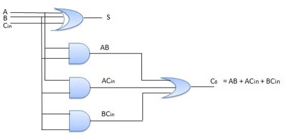
Fig. Full adder
Key Takeaways:
- Half adder is a combinational circuit which has two inputs and two outputs.
- Since there is no provision for carry in half adder, full adder is developed to overcome the drawback.
Subtractor
Half Subtractors
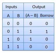
It is a combination circuit with two inputs and two outputs.
The difference between the two binary bits is obtained at the output and an output (Borrow) indicates if a 1 has been borrowed.
Here A is called as Minuend bit and B is called as Subtrahend bit.
Truth Table
Circuit Diagram
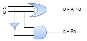
Fig. Half subtractor
Full Subtractors
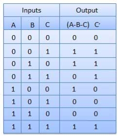
It is a combinational circuit which has three inputs A,B,C and two output D and C'.
A is the 'minuend', B is 'subtrahend', C is the 'borrow' which is produced by the previous stage, difference output D and C' is the borrow output.
Truth Table
Circuit Diagram
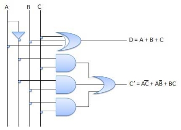
Fig. Full subtractor
Key Takeaways:
- Half subtractor is a combinational circuit which has two inputs and two outputs.
- Since there is no provision for borrow in half subtractor, full subtractor is developed to overcome the drawback.
BCD Adder
BCD stands for binary coded decimal.
Suppose, we have two 4-bit numbers A and B. The value of A and B can vary from 0(0000 in binary) to 9(1001 in binary).
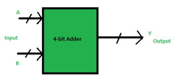
Fig.: BCD adder
- The output varies from 0 to 18 if the carry from the previous sum is not considered.
- But if we consider the carry, then the maximum value of output will be 19 (i.e., 9+9+1 = 19).
- When we simply add A and B, then we get the binary sum, and to get the output in BCD form, we use BCD Adder.
Example 1:
Input:
A = 0111 B = 1000
Output:
Y = 1 0101
Explanation: We are adding A (=7) and B (=8).
The value of the binary sum will be 1111(=15).
But the BCD sum will be 1 0101,
Where 1 is 0001 in binary and 5 is 0101 in binary.
Example 2:
Input:
A = 0101 B = 1001
Output:
Y = 1 0100
Explanation: We are adding A (=5) and B (=9).
The value of the binary sum will be 1110(=14).
But the BCD sum will be 1 0100,
Where 1 is 0001 in binary and 4 is 0100 in binary.
Now, let's move to the table and find out the logic when we are going to add “0110”.
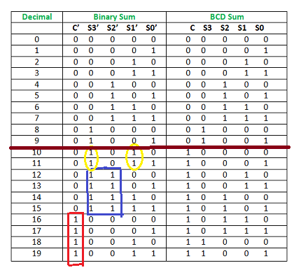
Fig.: Table explaining BCD addition
We are adding “0110” (=6) only to the second half of the table because of the following conditions:
- If C’ = 1 (Satisfies 16-19)
- If S3′. S2′ = 1 (Satisfies 12-15)
- If S3′. S1′ = 1 (Satisfies 10 and 11)
So, our logic is
C' + S3’. S2' + S3’. S1' = 1
Implementation:
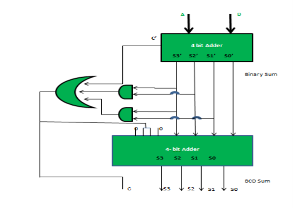
Fig.: BCD adder (ref. 2)
- An ALU performs mathematical and logical operations on binary numbers.
- They are located at the heart of every digital computer system and are one of the most important parts of a CPU (Central Processing Unit).
- Fetch-decode-execute refers to a computational process that continuously fetches the instructions from a memory, decodes them into operations and executes them to perform a calculation.
- These are simple steps which give rise to the complex behaviours that we expect from modern computing machines.
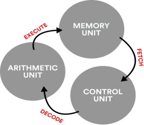
Fig. An illustration of the fetch-decode-execute cycle
This process can be further explained by linking each cycle step with three hardware subsystems called as a memory unit, a control unit, and an arithmetic unit.
References:
1. Modern digital Electronics- R. P. Jain, McGraw Hill.
2. Digital Integrated Electronics- Herbert Taub, McGraw Hill.
3. Digital Logic and Computer Design- Morris Mano (PHI).
4. Digital Integrated Electronics- Herbert Taub, McGraw Hill.
5. Digital Electronics Logic and System – James Bingnell and Robert Donovan, Cengage Learning.