Unit - 4
Architecture & Programming of 8085

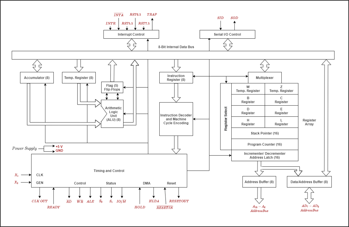
Fig. 8085 microprocessor architecture
8085 consists of the following functional units −
Accumulator
The accumulator is an 8-bit register used to perform arithmetic, logical, I/O & LOAD/STORE operations. It is connected to internal data bus & ALU.
Arithmetic and logic unit
The arithmetic and logic unit performs arithmetic and logical operations like Addition, Subtraction, AND, OR, etc. on 8-bit data.
General purpose register
8085 consists of six general purpose registers in 8085 processor that is B, C, D, E, H & L. Each register holds 8-bit data. These registers work in pair to hold 16-bit data and their pairing combination is like B-C, D-E & H-L.
Program counter
It is a 16-bit register used to store the memory address location of the next instruction to be executed. Microprocessor increments the program whenever an instruction is being executed, so that the program counter points to the memory address of the next instruction that is going to be executed.
Stack pointer
It is 16-bit register which works like stack, which gets incremented/decremented by 2 during push & pop operations.
Temporary register
It is an 8-bit register, which holds the temporary data of arithmetic and logical operations.
Flag register
It is an 8-bit register which holds 0 or 1 depending upon the result stored in the accumulator.
These are:
- Sign (S)
- Zero (Z)
- Auxiliary Carry (AC)
- Parity (P)
- Carry (C)

Instruction registers and decoder
It is an 8-bit register. When an instruction is fetched from memory then it is stored in the Instruction register. Instruction decoder decodes the information present in the Instruction register.
Timing and control unit
It provides timing and control signal to the microprocessor to perform operations. Following are the timing and control signals, which control external and internal circuits −
- Control Signals: READY, RD’, WR’, ALE
- Status Signals: S0, S1, IO/M’
- DMA Signals: HOLD, HLDA
- RESET Signals: RESET IN, RESET OUT
Interrupt control
It controls the interrupts during the process. When the microprocessor is executing the main program and whenever an interrupt occurs, the microprocessor shifts the control from the main program to process the incoming request. After the request is completed, the control returns to the main program.
There are 5 interrupt signals in 8085 microprocessors:
- INTR
- RST 7.5
- RST 6.5
- RST 5.5
- TRAP.
Serial Input/output control
It controls the serial data communication by using the two instructions: SID (Serial input data) and SOD (Serial output data).
Address buffer and address-data buffer
The content stored in the stack pointer and program counter is loaded into the address buffer and address-data buffer to communicate with the CPU.
The memory and I/O chips are connected to these buses, the CPU can exchange the desired data with the memory and I/O chips.
Address bus and data bus
Data bus carries the data to be stored. It is bidirectional whereas address bus carries the location to where it should be stored, and it is unidirectional. It is used to transfer the data & Address I/O devices.
Addressing modes of 8085
The instructions are used to transfer the data from one register to another register, from the memory to the register, and from the register to the memory without any change in the content.
Addressing modes in 8085 is divided into 5 groups −
Immediate addressing mode
Here, the 8/16-bit data is specified in the instruction itself as one of its operand. For example: MVI B, 40F means 40F is copied into register B.
Register addressing mode
Here, the data is copied from one register to another.
For example: MOV B, A: means data in register A is copied to register B.
Direct addressing mode
Here, the data is directly copied from the given address to the register.
For example: LDB 5008H: means the data at address 5008H is copied to register B.
Indirect addressing mode
Here, the data is transferred from one register to another by using the address pointed by the register.
For example: MOV B, K: means data is transferred from the memory address pointed by the register K to the register B.
Implied addressing mode
Here, it doesn’t require any operand; the data is specified by the opcode itself.
For example: CMP.
An instruction is a binary pattern designed inside a microprocessor to perform a specific function.
- The entire group of instructions that a microprocessor supports is called Instruction Set.
- 8085 has 246instructions.
- Each instruction is represented by an 8-bit binary value.
- These 8-bits of binary value is called Op-Code or Instruction Byte.
It is classified into 5 groups:
Data Transfer Instruction
These instructions transfer data between registers or between memory and registers. The instruction is used to copy data from source to destination while copying the contents of source cannot be modified.
OPCODE | OPERAND | DESCRIPTION |
MOV | Rd, Rs Rd, M M, Rs | Transfer the contents of the source to the destination. |
MVI | Rd, data M, data | Move immediate data into the destination register |
LXI | Reg. Pair, data | Move 16 bit data into the register pair |
LDA | 16 bit address | Load accumulator with data present at the specified address |
XCHG | - | Exchange the contents of HL with DE |
For example
MOV B,C
MVI B,20H
LXI H, 4020H
LDA 6000H
Arithmetic Instructions
- Addition
- Subtraction
- Increment
- Decrement
OPCODE | OPERAND | DESCRIPTION |
ADD | R M | Add the contents of register with the contents of accumulator and save in accumulator. |
ADC | R M | Add the contents of register with the contents of accumulator with carry and save in accumulator. |
ADI | 8 bit data | Add data with the content of acc |
DAD | Reg pair | Add register pair to H-L pair |
SUB | R M | Subtract the contents of register with the contents of accumulator and save in accumulator. |
SBB | R M | Subtract the contents of register with borrow from the contents of accumulator and save in accumulator. |
SUI | 8 bit data | Subtract data with the content of acc |
INR | R M | Increment register or memory by 1 |
DCR | R M | Decrement register or memory by 1 |
For example:
ADD C
ADC M
ADI 40H
DAD HL
SUB B
SUI 20H
INR C
Logical Instructions
The logical operations are:
- AND
- OR
- XOR
- Rotate
- Compare
- Complement
OPCODE | OPERAND | DESCRIPTION |
CMP | R M | Compare the contents of register or memory with accumulator |
ANA | R M | Logical AND the contents of register with accumulator |
ANI | 8 bit data | Logical AND the data with accumulator |
XRA | R M | XOR the contents of register with accumulator |
ORA | R M | Logical OR the contents of register with accumulator |
RLC | - | Rotate accumulator left |
RRC | - | Rotate accumulator right |
CMA | - | Complement accumulator |
For example
CMP C
ANA B
ANI 40H
XRA M
ORA C
RLC
Branching Instructions
These instructions alter the normal sequential flow conditionally or unconditionally
OPCODE | OPERAND | DESCRIPTION |
JMP | 16 bit address | Jump unconditionally to the given location |
JC | 16 bit address | Jump if carry |
JNC | 16 bit address | Jump if no carry |
JZ | 16 bit address | Jump if zero |
JNZ | 16 bit address | Jump if no zero |
CALL | 16 bit address | Call unconditionally |
RET | - | Return unconditionally |
RST | 0-7 | Restart (Software Interrupts) |
For example
JMP 2000H
RET
RST 6
Control Instructions
It controls the operation of microprocessor
OPCODE | OPERAND | DESCRIPTION |
NOP | - | No operation |
HLT | - | Halt |
DI | - | Disable Interrupt |
EI | - | Enable Interrupt |
RIM | - | Read interrupt mask |
SIM | - | Set interrupt mask |
For example
NOP
EI
SIM
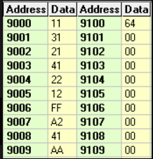
Let us suppose that 10 data are stored in memory location from 9000H to 9009H. These data are to be added and let us store the result in memory location 9100H.
Algorithm:
Start.
- Load into register pair HL from memory location 9000H.
- Load into register pair DE from memory location 9100H.
- Move 09 into register C as counter.
- Move the content of memory M into accumulator A.
- Increment register pair HL by 1.
- Add content of memory M with the contents of the accumulator A.
- Decrement value of register C by 1.
- If no zero is present, go to step 6 else go to step 10.
- Store the content of accumulator A into memory location pointed by register pair DE.
- Terminate the program.
Program Code:
LXI H, 9000H
LXI D, 9100H
MVI C, 09H
MVI B, 00H
MOV A, M
UP:
INX H
ADD M
JNC DOWN
INR B
DOWN:
DCR C
JNZ UP
STAX D
MOV A, B
STA 9101H
HLT

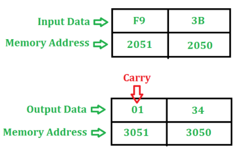
Write an assembly language program to add two 8-bit numbers stored at address 2050 and address 2051 in 8085 microprocessor. The starting address of the program is taken as 2000.
- Load the first number from memory location 2050 to accumulator.
- Move the content of accumulator to register H.
- Load the second number from memory location 2051 to accumulator.
- Then add the content of register H and accumulator using “ADD” instruction and storing result at 3050
- The carry generated is recovered using “ADC” command and is stored at memory location 3051
Program –
Memory Address | Mnemonics | Comment |
2000 | LDA 2050 | A<- [2050] |
2003 | MOV H, A | H<-A |
2004 | LDA 2051 | A<- [2051] |
2007 | ADD H | A<-A+H |
2008 | MOV L, A | L←A |
2009 | MVI A 00 | A←00 |
200B | ADC A | A←A+A+carry |
200C | MOV H, A | H←A |
200D | SHLD 3050 | H→3051, L→3050 |
2010 | HLT |
|

References:
1. 8 bit Microprocessor by Ramesh Gaonkar.
2. 8 bit microprocessor & controller by V. J. Vibhute, Techmak Publication.
3. Microprocessor and interfacing : Douglas Hall
4. Advanced Microprocessors And Peripherals A.K.Ray ,K.M.Bhuchandi
5. 8085 Microprocessor & its Applications by A. Nagoor Kani, Mc Graw Hill.