Unit - 2
Instruction Set and Programming
An Addressing Mode is a way to locate a target Data, which is also called as Operand. The 8051 Family of Microcontrollers allows five types of Addressing Modes for addressing the Operands. They are:
- Immediate Addressing
- Register Addressing
- Direct Addressing
- Register – Indirect Addressing
- Indexed Addressing
LABEL: (THIS IS NOT NECESSARY UNLESS THAT SPECIFIC LINE HAS TO BE ADDRESSED). The label is a symbolic address for the instruction. When the program is assembled, the label will be given specific address in which that instruction is stored. Unless that specific line of instruction is needed by a branching instruction in the program, it is not necessary to label that line.
OPCODE: Opcode is the symbolic representation of the operation. The assembler converts the opcode to a unique binary code (machine language).
OPERAND: While opcode specifies what operation to perform, operand specifies where to perform that action. The operand field generally contains the source and destination of the data. In some cases, only source or destination will be available instead of both. The operand will be either address of the data, or data itself.
COMMENT: Always comment will begin with; or // symbol. To improve the program quality, programmer may always use comments in the program.
The following section explains the Basic data types for 8051.
Data Type:
- 8051-microcontroller has only one data type - 8 bits.
- The size of each register is also 8 bits
- It is the job of the programmer to break down data larger than 8 bits (00 to FFH, or 0 to 255 in decimal)
- The data types can be positive or negative
In Immediate Addressing mode, the operand, which follows the Opcode, is a constant data of either 8 or 16 bits. The name Immediate Addressing came from the fact that the constant data to be stored in the memory immediately follows the Opcode. The constant value to be stored is specified in the instruction itself rather than taking from a register. The destination registers to which the constant data must be copied should be the same size as the operand mentioned in the instruction.
Example: MOV A, #030H Here, the Accumulator is loaded with 30 (hexadecimal).
The # in the operand indicates that it is a data and not the address of a Register. Immediate Addressing is very fast as the data to be loaded is given in the instruction itself.
In the 8051 Microcontroller Memory Organization, we have seen the organization of RAM and four banks of Working Registers with eight Registers in each bank. In Register Addressing mode, one of the eight registers (R0 – R7) is specified as Operand in the Instruction. It is important to select the appropriate Bank with the help of PSW Register. Let us see a example of Register Addressing assuming that Bank0 is selected.
Example: MOV A, R5 Here, the 8-bit content of the Register R5 of Bank0 is moved to the Accumulator.
In Direct Addressing Mode, the address of the data is specified as the Operand in the instruction. Using Direct Addressing Mode, we can access any register or on-chip variable. This includes general purpose RAM, SFRs, I/O Ports, Control registers.
Example: MOV A, 47H Here, the data in the RAM location 47H is moved to the Accumulator.
In the Indirect Addressing Mode or Register Indirect Addressing Mode, the address of the Operand is specified as the content of a Register. This will be clearer with an example.
Example: MOV A, @R1
The @ symbol indicates that the addressing mode is indirect. If the contents of R1 is 56H, for example, then the operand is in the internal RAM location 56H.
If the contents of the RAM location 56H is 24H, then 24H is moved into accumulator. Only R0 and R1 are allowed in Indirect Addressing Mode. These register in the indirect addressing mode are called as Pointer registers.
Relative addressing is used only with certain jump instructions. A relative address is an 8-bit signed value, which is added to the program counter to form the address of the next instruction executed. Since, an 8-bit signed offset is used, the range of jumping is -128 to +127 locations. The relative offset is appended to the instruction as an additional byte.
Prior to the addition, the program counter is incremented to the address following jump instruction thus the new address is relative to the next instruction, not the address of the jump instruction.
Normally, this detail is of no concern to the programmer, since jump destinations are usually specified as labels and the assembler determines the relative offset accordingly. For example, if the label THERE represents an instruction at location 1040H and the instruction
SJMP THERE
Is in memory at location 1000H and 1001H, the assembler will assign a relative offset of 3EH as byte 2 of the instruction (1002H +3EH=1040H)
Relative addressing offers the advantage of providing position-independent code but the disadvantage that the jump destinations are limited in range.
With Indexed Addressing Mode, the effective address of the Operand is the sum of a base register and an offset register. The Base Register can be either Data Pointer (DPTR) or Program Counter (PC) while the Offset register is the Accumulator (A). In Indexed Addressing Mode, only MOVC and JMP instructions can be used. Indexed Addressing Mode is useful when retrieving data from look-up tables.
Example: MOVC A, @A+DPTR
In this addressing, the address of the flag which contains the operand, is implied in the opcode of the instruction.
Eg. CLR C; Clears the carry flag to 0
In this addressing mode the direct address of the bit is specified in the instruction. The RAM space 20H to 2FH and most of the special function registers are bit addressable. Bit address values are between 00H to 7FH.
Eg. CLR 07H; Clears the bit 7 of 20h RAM space
SETB 07H; Sets the bit 7 of 20H RAM space.
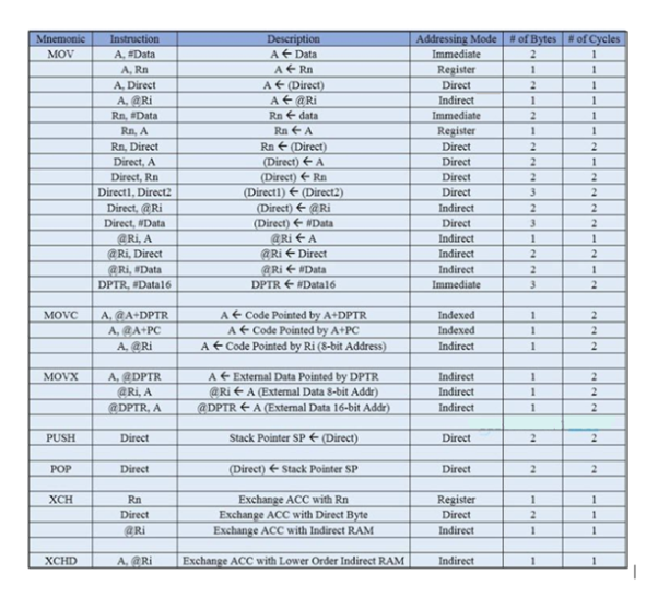
The Data Transfer Instructions relate to transfer of data between registers or external program memory or data memory. The Mnemonics associated with Data Transfer are given below.
- MOV
- MOVC
- MOVX
- PUSH
- POP
- XCH
- XCHD

Using Arithmetic Instructions, one can perform addition, subtraction, multiplication and division. It consists of increment by one, decrement by one and a special instruction called Decimal Adjust Accumulator.
The Mnemonics associated with the Arithmetic Instructions of the 8051 Microcontroller Instruction Set are:
- ADD
- ADDC
- SUBB
- INC
- DEC
- MUL
- DIV
- DA A
The arithmetic instructions have no knowledge about the data format that is signed, unsigned, ASCII, BCD, and so on. The operations performed by the arithmetic instructions affect flags like carry, overflow, zero, etc. in PSW Register.
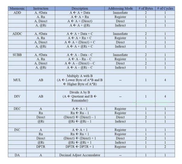
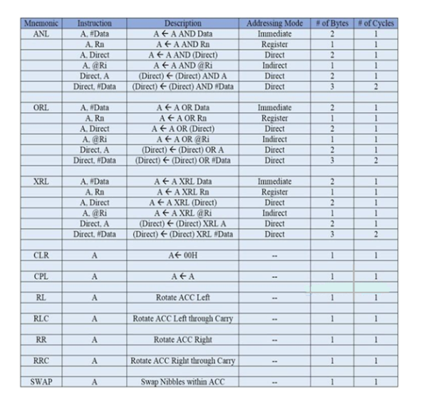
Logical Instructions perform logical operations like AND, OR, XOR, NOT, Rotate, Clear and Swap. Logical Instruction are performed on bytes of data on a bit-by-bit basis.
Mnemonics associated with Logical Instructions are as follows:
- ANL
- ORL
- XRL
- CLR
- CPL
- RL
- RLC
- RR
- RRC
- SWAP

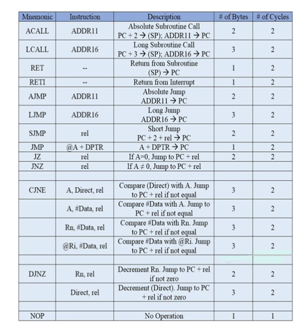
The logic of the program is controlled by these instructions. The mnemonics of the Program Branching Instructions are:
- LJMP
- AJMP
- SJMP
- JZ
- JNZ
- CJNE
- DJNZ
- NOP
- LCALL
- ACALL
- RET
- RETI
- JMP
All these instructions, except the NOP (No Operation) affect the Program Counter (PC) Some of these instructions have decision making capability before transferring control to other part of the program.
The following table shows all the mnemonics with respect to the program branching instructions.

Subroutines are handled by CALL and RET instructions There are two types of CALL instructions
1. LCALL address (16 bit)
This is long call instruction which unconditionally calls the subroutine located at the indicated 16 bit address. This is a 3 byte instruction. The LCALL instruction works as follows.
- During execution of LCALL, [PC] = [PC]+3; (if address where LCALL resides is say, 0x3254; during execution of this instruction [PC] = 3254h + 3h = 3257h
- [SP]=[SP]+1; (if SP contains default value 07, then SP increments and [SP]=08
- [[SP]] = [PC7-0]; (lower byte of PC content ie., 57 will be stored in memory location 08.
- [SP]=[SP]+1; (SP increments again and [SP]=09)
- [[SP]] = [PC15-8]; (higher byte of PC content ie., 32 will be stored in memory location 09. With these the address (0x3254) which was in PC is stored in stack.
- [PC]= address (16 bit);the new address of subroutine is loaded to PC. No flags are affected.
2. ACALL address (11 bit)
This is absolute call instruction which unconditionally calls the subroutine located at the indicated 11 bit address. This is a 2 byte instruction. The SCALL instruction works as follows.
- During execution of SCALL, [PC] = [PC]+2; (if address where LCALL resides is say, 0x8549; during execution of this instruction [PC] = 8549h + 2h = 854Bh
- [SP]=[SP]+1; (if SP contains default value 07, then SP increments and [SP]=08
- [[SP]] = [PC7-0]; (lower byte of PC content ie., 4B will be stored in memory location 08.
- [SP]=[SP]+1; (SP increments again and [SP]=09)
- [[SP]] = [PC15-8]; (higher byte of PC content ie., 85 will be stored in memory location 09. With these the address (0x854B) which was in PC is stored in stack.
- [PC10-0]= address (11 bit); the new address of subroutine is loaded to PC. No flags are affected.
RET instruction
RET instruction pops top two contents from the stack and load it to PC.
- [PC15-8] = [[SP]]; content of current top of the stack will be moved to higher byte of PC.
- [SP]=[SP]-1; (SP decrements)
- [PC7-0] = [[SP]]; content of bottom of the stack will be moved to lower byte of PC.
- [SP]=[SP]-1; (SP decrements again)
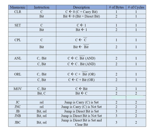
Boolean or Bit Manipulation Instructions will deal with bit variables. There is a special bit-addressable area in RAM and some Special Function Registers (SFRs) that are bit addressable.
The Mnemonics corresponding to the Boolean or Bit Manipulation instructions are:
- CLR
- SETB
- MOV
- JC
- JNC
- JB
- JNB
- JBC
- ANL
- ORL
- CPL
These instructions perform set, clear, and, or, complement at bit level. All the possible mnemonics of the Boolean Instructions are specified in the following table.
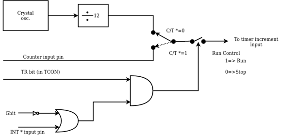
There are two 16-bit timer registers are known as Timer0 and Timer1. The timer registers are used as Timer mode and Counter mode. The only difference in these two modes is the source for incrementing the timer registers.
Timer Mode
In timer mode, it counts internal machine cycles. So, this register gets incremented for each machine cycle. When the clock frequency is 12MHz, timer register is incremented for every millisecond. It ignores external timer input pin in this mode.
Counter Mode
In counter mode, it counts external events. The timer register gets incremented for every 1 to 0 transition in the external input pin. This type of transitions is referred as events.
The external input pins are sampled once for each machine cycle. In order to determine 1or 0 transitions another machine cycle is required.
Therefore, atleast two machine cycles are required in this mode. When frequency is12MHz the maximum count frequency will be 12MHz/24 = 500KHz. So, for event counting time duration is 2 µs.
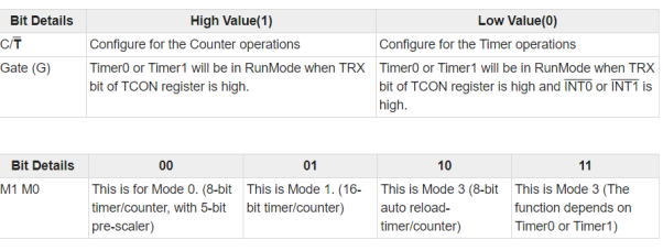
Timer or Counter has four different modes. Mode 0 to Mode 2 are for both Timer/Counter. Mode 3 represent different meaning for each timer register. There is a register called TMOD which can be programmed to configure these timers or counters.
The Serial port is used for serial communication in mode 1 and 3. For baud rate generation timer1 is used. Hence, Timer0 is available for timer or counter operations.
TMOD Register
TMOD(Timer Mode) is an SFR. The address of this register is 89H. This is not bit-addressable.

Mode 0 of Timer/Counter
Mode 0 operation is 8-bit timer or counter with 5-bit pre-scaler. It is 13-bit timer/counter. Which uses 5 bits of TL0 or TL1 and 8-bits of TH0 or TH1.

Fig. Mode 0
Mode 1 of Timer/Counter
Mode 1 operation is 16-bit timer or counter. In the following diagram, Mode 1 is used for Timer0.

Fig. Mode 1
Mode 2 of Timer/Counter
Mode 2 operation is 8-bit auto reload timer or counter. Mode 2 is used for Timer1.
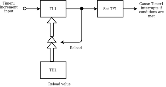
Fig. Mode 2
Mode 3 of Timer/Counter
Mode 3 is different for Timer0 and Timer1. When Timer0 is working in mode 3, TL0 will be used as 8-bit timer/counter. It will be controlled by standard Timer0 control bits, T0 and INT0 inputs. TH0 is used as 8-bit timer not counter. This is controlled by Timer1 Control bit TR1. When the TH0 overflows from FFH to 00H, TF1 is set to 1. In the following diagram, Timer0 is in Mode 3.

Figure. Mode 3
Operation:
- It controls the running of 8-bit timer/counter TL0 like Mode 0, 1, or 2. The running of TH0 is controlled by TR1 bit. So, the gate bit in this mode for Timer0 has no specific role.
- The mode 3 is present for applications requiring an extra 8-bit timer/counter. In Mode 3 of Timer0, 8051 has three timers. One 8-bit timer by TH0, another8-bit timer/counter by TL0, and one 16-bit timer/counter by Timer1.
- If Timer0 is in mode3, and Timer1 is working on either 0, 1 or 2, then the gun control of the Timer1 is activated when the gate bit is low or INT1 is high. The run control is deactivated when the gate is high and INT1 is low.
Key takeaway
Timer or Counter has four different modes. Mode 0 to Mode 2 is for both Timer/Counter. Mode 3 represent different meaning for each timer register. There is a register called TMOD which can be programmed to configure these timers or counters.
The Serial port is used for serial communication in mode 1 and 3. For baud rate generation timer1 is used. Hence, Timer0 is available for timer or counter operations.

Fig. Interrupt Structure of 8051
8051 has five interrupts. These are INT0, INT1, T0, T1, TI/RI. All these interrupts can be enabled or disabled by IE (interrupt enable) register.
Interrupt Enable (IE)Register
This register can be used to enable or disable interrupts by programming. It is an SFR with address A8H. This byte is bit addressable hence can be programmed by the user. Every bit in this register has a specific meaning.


Interrupt Priority (IP) Register
The five interrupts can be either one or two interrupt level. The priority levels are level 1 and level 0. Higher Priority is indicated by level 1 and level 0 indicates lower priority. To store priority levels for each interrupt IP register is used. This is bit addressable SFR with address B8H.


External Interrupt
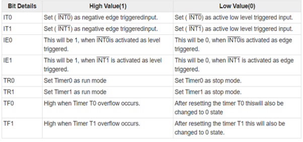
The external interrupts are INT0 and INT1. The TCON register can be used to program external interrupts to edge or level triggered. The TCON is Timer Control. TCON is another bit addressable SFR. The address is 88H.

Key takeaway
Interrupt is a subroutine call that interrupts the microcontroller's main operations or work and causes it to execute any other program, at the time of operation. It provides a mechanism to put on hold the ongoing operations, execute a subroutine and resume to another type of operation.
8051 has five interrupts as mentioned below:
- INTO
- TFO
- INT1
- TF1
- R1/T1
The interrupts (INT0) ̅ and (INT1) ̅ are called as external interrupts. The interrupts (INT0) ̅ and (INT1) ̅ are negative edge triggered. When, these interrupts are activated, the corresponding flags are set except for serial interrupts.
Exchange the content of FFH and FF00H
MOV dptr, #0FF00H ; take the address in dptr
MOVX A, @dptr ; get the content of 0050H in a
MOV r0, 0FFH ; save the content of 50H in r0
MOV 0FFH, a ; move a to 50H
MOV A, r0 ; get content of 50H in a
MOVX @dptr, a ; move it to 0050H
Store the higher nibble of r7 in to both nibbles of r6
Firstly, we get the upper nibble of r7 in r6. Then we swap nibbles of r7 and make OR operation with r6 so the upper and lower nibbles are duplicated
MOV A, r7 ; get the content in acc
ANI A, #0F0h ; mask lower bit
MOV r6, A ; send it to r6
SWAP A ; xchange upper and lower nibbles of accumulator
ORL A, r6 ; OR operation
MOV r6, A ; finally load content in r6
Transfer the block of data from 20H to 30H to external location 1020H to 1030H.
MOV r7, #0AH ; initialize counter by 10d
MOV r0, #20H ; get initial source location
Mov dptr, #1020H ; get initial destination location
Nxt: MOV A, @r0 ; get first content in acc
MOVX @dptr, a ; move it to external location
INC r0 ; increment source location
INC dptr ; increase destination location
DJNZ r7, nxt ; decrease r7. If zero then over otherwise move next
Given block of 100h to 200h. Find out how many bytes from this block are greater then, the number in r2 and less then number in r3. Store the count in r4.
MOV dptr, #0100H ; get initial location
MOV r7, #0FFH ; counter
MOV r4, #00H ; number counter
MOV 20H, R2 ; get the upper and lower limits in
MOV 21H, R3 ; 20H and 21H
Nxt: MOVX A, @dptr ; get the content in acc
CJNE A, 21H, lower ; check the upper limit first
SJMP out ; if number is larger
Lower: JNC out ; jump out
CJNE A, 20H, limit ; check lower limit
SJMP out ; if number is lower
Limit: JC out ; jump out
INC r4 ; if number within limit increment count
Out: INC dptr ; get next location
DJNZ r7, nxt ; repeat until block completes
Find out how many equal bytes between two memory blocks 10H to 20H and 20H to 30H.
MOV r7, #0AH ; initialize counter by 10d
MOV r0, #10H ; get initial location of block1
MOV r1, #20H ; get initial location of block2
MOV r6, #00H ; equal byte counter. Starts from zero
Nxt: MOV A, @r0 ; get content of block 1 in acc
MOV b, a ; move it to B
MOV A, @r1 ; get content of block 2 in acc
CJNE A, B, nomatch ; compare both if equal
INC r6 ; increment the counter
Nomatch: INC r0 ; otherwise go for second number
INC r1
DJNZ r7, nxt ; decrease r7. If zero then over otherwise move next
Write a test program for the DS89C420/30 chip to toggle all the bits of PO, PI, and P2 every 1/4 of a second. Assume a crystal frequency of 11.0592 MHz.
ORG 0
BACK: MOV A,#55H
MOV P0, A
MOV P1, A
MOV P2, A
ACALL QSDELAY
SJUMP BACK
QSDELAY:
MOV R5, #11
H3: MOV R4, #248
H2: MOV R3, #255
H1: DJNZ R3, H1
DJNZ R4, H2,
DJUNZ R5, H3
Delay = 11 x 248 x 255 x 4MC x 90ns = 250,430 s
s
Create a square wave of 50% duty cycle on bit 0 of port 1.
The 50% duty cycle means that the "on" and "off' states (or the high and low
Portions of the pulse) have the same length. Therefore, we toggle Pl.0 with a
Time delay in between each state.
HERE: SETB P1.0
LCALL
CLR PI. 0
LCALL DELAY
SJMP HERE
Another way to write the above program is:
HERE: CPL P1.0
LCALL DELAY
SJMP HERE
Create a square wave of 66% duty cycle on bit 3 of port 1
BACK: SETB Pl.3
LCALL DELAY
LCALL DELAY
CLR P1.3
LCALL DELAY
SJMP BACK
Write a program to perform the following:
(a) keep monitoring the Pl.2 bit until it becomes high
(b) when P 1.2 becomes high, write value 45H to port 0
(c) send a high-to-Iow (H-to-L) pulse to P2,3
SETB PI.2
MOV A,#45H
AGAIN JNB PI.2,AGAIN
MOV PO ,A
SETB P2.3
CLR P2.3
In this program, instruction "JNB PI 2 AGAING” (JNB means Jump if no bit) stays in the loop as long as P 1.2 is low. When P.12 becomes high. It gets out of the loop. Writes the value 45H to port 0 and creates an H-to-L pulse by the sequence of instruction SETB and CLR.
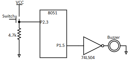
Assume that bit P2.3 is an input and represents the condition of an oven. If it goes high, it means that the oven is hot. Monitor the bit continuously. Whenever it goes high, send a high-to-low pulse to port P 1.5 to tum on a buzzer.
HERE: JNB P2.3, HERE
SETB Pl. 5
CLR Pl. 5
SJMP HERE

A switch is connected to pin P 1.7. Write a program to check the status of SW and perform
The following:
(a) If SW=O, send letter 'N' to P2.
(b) If SW=I, send letter 'Y'toP2.
SETB Pl.?
AGAIN JB Pl.2,OVER
MOV P2,#'N'
SJMP AGAIN
OVER MOV P2,#'Y'
SJMP AGAIN
A switch is connected to pin PI. 7. Write a program to check the status of the switch and
Perform the following:
(a) If switch = 0, send letter 'N' to P2.
(b) If switch = I, send letter 'Y'toP2.
SET P1.7
AGAIN: MOV C, P1.2
JC OVER
OVER: MOV P2, #’N’
SJMP AGAIN
A switch is connected to pin P1.0 and an LED to pin P2.7 status of the switch and send it to the LED
SET P1.7
AGAIN: MOV C, P1.0
MOV P2.7, C
SJMP AGAIN
Program to transfer letter “D” serially at 9800baud, continuously:
MOV TMOD,#20H ; timer 1,mode 2(auto reload)
MOV TH1, #-3 ; 9600 baud rate
MOV SCON, #50H ; 8-bit, 1 stop, REN enabled
SETB TR1 ; start timer 1
AGAIN: MOV SBUF, #”D” ; letter “D” to transfer
HERE: JNB TI, HERE ; wait for the last bit
CLR TI ;clear TI for next char
SJMP AGAIN ; keep sending A
Steps to receive data serially:
1. Set baud rate by loading TMOD register with value 20H, to indicates that timer 1 is in mode2 (8-bit auto-reload) and set baud rate
2. TH1 is loaded with value to set baud rate.
3. The SCON register is loaded with value 50H, indicating serial mode 1, where an 8- bit data is framed with start and stop bits.
4. TR1 is set to 1 to start timer 1.
5. RI is cleared by CLR RI instruction
6. The RI flag bit is monitored by JNB RI instruction to see if an entire character has been received .
7. When RI is raised, SBUF has a byte, its contents are moved into to safe place.
8. To receive next character, jump to step 5
Program to receive bytes of data serially, and put them in P2, set the baud rate at 9600, 8-bit data, and 1stop bit:
MOV TMOD, #20H ; timer 1,mode 2(auto reload)
MOV TH1, #-3 ; 9600 baud rate
MOV SCON, #50H ; 8-bit, 1 stop, REN enabled
SETB TR1 ; start timer 1
HERE: JNB RI, HERE ; wait for char to come in
MOV A, SBUF ; saving incoming byte in A
MOV P2, A ; send to port 1
CLR RI ; get ready to receive next byte
SJMP HERE ; keep getting data
References:
1. M. A.Mazidi, J. G. Mazidi and R. D. McKinlay, “The8051Microcontroller and Embedded Systems: Using Assembly and C”, Pearson Education, 2007.
2. K. J. Ayala, “8051 Microcontroller”, Delmar Cengage Learning,2004.
3. The 8051 Microcontroller Based Embedded System By Manish K. Patel TMH.
4. Embedded System Architecture, Programming and Design by Raj Kamal, 3rd Edition TMH.
5. Introduction to Embedded System by Shibu K. V. 3rd Edition TMH
Unit - 2
Instruction Set and Programming
An Addressing Mode is a way to locate a target Data, which is also called as Operand. The 8051 Family of Microcontrollers allows five types of Addressing Modes for addressing the Operands. They are:
- Immediate Addressing
- Register Addressing
- Direct Addressing
- Register – Indirect Addressing
- Indexed Addressing
LABEL: (THIS IS NOT NECESSARY UNLESS THAT SPECIFIC LINE HAS TO BE ADDRESSED). The label is a symbolic address for the instruction. When the program is assembled, the label will be given specific address in which that instruction is stored. Unless that specific line of instruction is needed by a branching instruction in the program, it is not necessary to label that line.
OPCODE: Opcode is the symbolic representation of the operation. The assembler converts the opcode to a unique binary code (machine language).
OPERAND: While opcode specifies what operation to perform, operand specifies where to perform that action. The operand field generally contains the source and destination of the data. In some cases, only source or destination will be available instead of both. The operand will be either address of the data, or data itself.
COMMENT: Always comment will begin with; or // symbol. To improve the program quality, programmer may always use comments in the program.
The following section explains the Basic data types for 8051.
Data Type:
- 8051-microcontroller has only one data type - 8 bits.
- The size of each register is also 8 bits
- It is the job of the programmer to break down data larger than 8 bits (00 to FFH, or 0 to 255 in decimal)
- The data types can be positive or negative
In Immediate Addressing mode, the operand, which follows the Opcode, is a constant data of either 8 or 16 bits. The name Immediate Addressing came from the fact that the constant data to be stored in the memory immediately follows the Opcode. The constant value to be stored is specified in the instruction itself rather than taking from a register. The destination registers to which the constant data must be copied should be the same size as the operand mentioned in the instruction.
Example: MOV A, #030H Here, the Accumulator is loaded with 30 (hexadecimal).
The # in the operand indicates that it is a data and not the address of a Register. Immediate Addressing is very fast as the data to be loaded is given in the instruction itself.
In the 8051 Microcontroller Memory Organization, we have seen the organization of RAM and four banks of Working Registers with eight Registers in each bank. In Register Addressing mode, one of the eight registers (R0 – R7) is specified as Operand in the Instruction. It is important to select the appropriate Bank with the help of PSW Register. Let us see a example of Register Addressing assuming that Bank0 is selected.
Example: MOV A, R5 Here, the 8-bit content of the Register R5 of Bank0 is moved to the Accumulator.
In Direct Addressing Mode, the address of the data is specified as the Operand in the instruction. Using Direct Addressing Mode, we can access any register or on-chip variable. This includes general purpose RAM, SFRs, I/O Ports, Control registers.
Example: MOV A, 47H Here, the data in the RAM location 47H is moved to the Accumulator.
In the Indirect Addressing Mode or Register Indirect Addressing Mode, the address of the Operand is specified as the content of a Register. This will be clearer with an example.
Example: MOV A, @R1
The @ symbol indicates that the addressing mode is indirect. If the contents of R1 is 56H, for example, then the operand is in the internal RAM location 56H.
If the contents of the RAM location 56H is 24H, then 24H is moved into accumulator. Only R0 and R1 are allowed in Indirect Addressing Mode. These register in the indirect addressing mode are called as Pointer registers.
Relative addressing is used only with certain jump instructions. A relative address is an 8-bit signed value, which is added to the program counter to form the address of the next instruction executed. Since, an 8-bit signed offset is used, the range of jumping is -128 to +127 locations. The relative offset is appended to the instruction as an additional byte.
Prior to the addition, the program counter is incremented to the address following jump instruction thus the new address is relative to the next instruction, not the address of the jump instruction.
Normally, this detail is of no concern to the programmer, since jump destinations are usually specified as labels and the assembler determines the relative offset accordingly. For example, if the label THERE represents an instruction at location 1040H and the instruction
SJMP THERE
Is in memory at location 1000H and 1001H, the assembler will assign a relative offset of 3EH as byte 2 of the instruction (1002H +3EH=1040H)
Relative addressing offers the advantage of providing position-independent code but the disadvantage that the jump destinations are limited in range.
With Indexed Addressing Mode, the effective address of the Operand is the sum of a base register and an offset register. The Base Register can be either Data Pointer (DPTR) or Program Counter (PC) while the Offset register is the Accumulator (A). In Indexed Addressing Mode, only MOVC and JMP instructions can be used. Indexed Addressing Mode is useful when retrieving data from look-up tables.
Example: MOVC A, @A+DPTR
In this addressing, the address of the flag which contains the operand, is implied in the opcode of the instruction.
Eg. CLR C; Clears the carry flag to 0
In this addressing mode the direct address of the bit is specified in the instruction. The RAM space 20H to 2FH and most of the special function registers are bit addressable. Bit address values are between 00H to 7FH.
Eg. CLR 07H; Clears the bit 7 of 20h RAM space
SETB 07H; Sets the bit 7 of 20H RAM space.
The Data Transfer Instructions relate to transfer of data between registers or external program memory or data memory. The Mnemonics associated with Data Transfer are given below.
- MOV
- MOVC
- MOVX
- PUSH
- POP
- XCH
- XCHD
Using Arithmetic Instructions, one can perform addition, subtraction, multiplication and division. It consists of increment by one, decrement by one and a special instruction called Decimal Adjust Accumulator.
The Mnemonics associated with the Arithmetic Instructions of the 8051 Microcontroller Instruction Set are:
- ADD
- ADDC
- SUBB
- INC
- DEC
- MUL
- DIV
- DA A
The arithmetic instructions have no knowledge about the data format that is signed, unsigned, ASCII, BCD, and so on. The operations performed by the arithmetic instructions affect flags like carry, overflow, zero, etc. in PSW Register.

Logical Instructions perform logical operations like AND, OR, XOR, NOT, Rotate, Clear and Swap. Logical Instruction are performed on bytes of data on a bit-by-bit basis.
Mnemonics associated with Logical Instructions are as follows:
- ANL
- ORL
- XRL
- CLR
- CPL
- RL
- RLC
- RR
- RRC
- SWAP
The logic of the program is controlled by these instructions. The mnemonics of the Program Branching Instructions are:
- LJMP
- AJMP
- SJMP
- JZ
- JNZ
- CJNE
- DJNZ
- NOP
- LCALL
- ACALL
- RET
- RETI
- JMP
All these instructions, except the NOP (No Operation) affect the Program Counter (PC) Some of these instructions have decision making capability before transferring control to other part of the program.
The following table shows all the mnemonics with respect to the program branching instructions.
Subroutines are handled by CALL and RET instructions There are two types of CALL instructions
1. LCALL address (16 bit)
This is long call instruction which unconditionally calls the subroutine located at the indicated 16 bit address. This is a 3 byte instruction. The LCALL instruction works as follows.
- During execution of LCALL, [PC] = [PC]+3; (if address where LCALL resides is say, 0x3254; during execution of this instruction [PC] = 3254h + 3h = 3257h
- [SP]=[SP]+1; (if SP contains default value 07, then SP increments and [SP]=08
- [[SP]] = [PC7-0]; (lower byte of PC content ie., 57 will be stored in memory location 08.
- [SP]=[SP]+1; (SP increments again and [SP]=09)
- [[SP]] = [PC15-8]; (higher byte of PC content ie., 32 will be stored in memory location 09. With these the address (0x3254) which was in PC is stored in stack.
- [PC]= address (16 bit);the new address of subroutine is loaded to PC. No flags are affected.
2. ACALL address (11 bit)
This is absolute call instruction which unconditionally calls the subroutine located at the indicated 11 bit address. This is a 2 byte instruction. The SCALL instruction works as follows.
- During execution of SCALL, [PC] = [PC]+2; (if address where LCALL resides is say, 0x8549; during execution of this instruction [PC] = 8549h + 2h = 854Bh
- [SP]=[SP]+1; (if SP contains default value 07, then SP increments and [SP]=08
- [[SP]] = [PC7-0]; (lower byte of PC content ie., 4B will be stored in memory location 08.
- [SP]=[SP]+1; (SP increments again and [SP]=09)
- [[SP]] = [PC15-8]; (higher byte of PC content ie., 85 will be stored in memory location 09. With these the address (0x854B) which was in PC is stored in stack.
- [PC10-0]= address (11 bit); the new address of subroutine is loaded to PC. No flags are affected.
RET instruction
RET instruction pops top two contents from the stack and load it to PC.
- [PC15-8] = [[SP]]; content of current top of the stack will be moved to higher byte of PC.
- [SP]=[SP]-1; (SP decrements)
- [PC7-0] = [[SP]]; content of bottom of the stack will be moved to lower byte of PC.
- [SP]=[SP]-1; (SP decrements again)
Boolean or Bit Manipulation Instructions will deal with bit variables. There is a special bit-addressable area in RAM and some Special Function Registers (SFRs) that are bit addressable.
The Mnemonics corresponding to the Boolean or Bit Manipulation instructions are:
- CLR
- SETB
- MOV
- JC
- JNC
- JB
- JNB
- JBC
- ANL
- ORL
- CPL
These instructions perform set, clear, and, or, complement at bit level. All the possible mnemonics of the Boolean Instructions are specified in the following table.

There are two 16-bit timer registers are known as Timer0 and Timer1. The timer registers are used as Timer mode and Counter mode. The only difference in these two modes is the source for incrementing the timer registers.
Timer Mode
In timer mode, it counts internal machine cycles. So, this register gets incremented for each machine cycle. When the clock frequency is 12MHz, timer register is incremented for every millisecond. It ignores external timer input pin in this mode.
Counter Mode
In counter mode, it counts external events. The timer register gets incremented for every 1 to 0 transition in the external input pin. This type of transitions is referred as events.
The external input pins are sampled once for each machine cycle. In order to determine 1or 0 transitions another machine cycle is required.
Therefore, atleast two machine cycles are required in this mode. When frequency is12MHz the maximum count frequency will be 12MHz/24 = 500KHz. So, for event counting time duration is 2 µs.
Timer or Counter has four different modes. Mode 0 to Mode 2 are for both Timer/Counter. Mode 3 represent different meaning for each timer register. There is a register called TMOD which can be programmed to configure these timers or counters.
The Serial port is used for serial communication in mode 1 and 3. For baud rate generation timer1 is used. Hence, Timer0 is available for timer or counter operations.
TMOD Register
TMOD(Timer Mode) is an SFR. The address of this register is 89H. This is not bit-addressable.


Mode 0 of Timer/Counter
Mode 0 operation is 8-bit timer or counter with 5-bit pre-scaler. It is 13-bit timer/counter. Which uses 5 bits of TL0 or TL1 and 8-bits of TH0 or TH1.

Fig. Mode 0
Mode 1 of Timer/Counter
Mode 1 operation is 16-bit timer or counter. In the following diagram, Mode 1 is used for Timer0.

Fig. Mode 1
Mode 2 of Timer/Counter
Mode 2 operation is 8-bit auto reload timer or counter. Mode 2 is used for Timer1.

Fig. Mode 2
Mode 3 of Timer/Counter
Mode 3 is different for Timer0 and Timer1. When Timer0 is working in mode 3, TL0 will be used as 8-bit timer/counter. It will be controlled by standard Timer0 control bits, T0 and INT0 inputs. TH0 is used as 8-bit timer not counter. This is controlled by Timer1 Control bit TR1. When the TH0 overflows from FFH to 00H, TF1 is set to 1. In the following diagram, Timer0 is in Mode 3.

Figure. Mode 3
Operation:
- It controls the running of 8-bit timer/counter TL0 like Mode 0, 1, or 2. The running of TH0 is controlled by TR1 bit. So, the gate bit in this mode for Timer0 has no specific role.
- The mode 3 is present for applications requiring an extra 8-bit timer/counter. In Mode 3 of Timer0, 8051 has three timers. One 8-bit timer by TH0, another8-bit timer/counter by TL0, and one 16-bit timer/counter by Timer1.
- If Timer0 is in mode3, and Timer1 is working on either 0, 1 or 2, then the gun control of the Timer1 is activated when the gate bit is low or INT1 is high. The run control is deactivated when the gate is high and INT1 is low.
Key takeaway
Timer or Counter has four different modes. Mode 0 to Mode 2 is for both Timer/Counter. Mode 3 represent different meaning for each timer register. There is a register called TMOD which can be programmed to configure these timers or counters.
The Serial port is used for serial communication in mode 1 and 3. For baud rate generation timer1 is used. Hence, Timer0 is available for timer or counter operations.
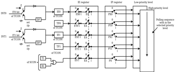
Fig. Interrupt Structure of 8051
8051 has five interrupts. These are INT0, INT1, T0, T1, TI/RI. All these interrupts can be enabled or disabled by IE (interrupt enable) register.
Interrupt Enable (IE)Register
This register can be used to enable or disable interrupts by programming. It is an SFR with address A8H. This byte is bit addressable hence can be programmed by the user. Every bit in this register has a specific meaning.


Interrupt Priority (IP) Register
The five interrupts can be either one or two interrupt level. The priority levels are level 1 and level 0. Higher Priority is indicated by level 1 and level 0 indicates lower priority. To store priority levels for each interrupt IP register is used. This is bit addressable SFR with address B8H.


External Interrupt
The external interrupts are INT0 and INT1. The TCON register can be used to program external interrupts to edge or level triggered. The TCON is Timer Control. TCON is another bit addressable SFR. The address is 88H.
Key takeaway
Interrupt is a subroutine call that interrupts the microcontroller's main operations or work and causes it to execute any other program, at the time of operation. It provides a mechanism to put on hold the ongoing operations, execute a subroutine and resume to another type of operation.
8051 has five interrupts as mentioned below:
- INTO
- TFO
- INT1
- TF1
- R1/T1
The interrupts (INT0) ̅ and (INT1) ̅ are called as external interrupts. The interrupts (INT0) ̅ and (INT1) ̅ are negative edge triggered. When, these interrupts are activated, the corresponding flags are set except for serial interrupts.
Exchange the content of FFH and FF00H
MOV dptr, #0FF00H ; take the address in dptr
MOVX A, @dptr ; get the content of 0050H in a
MOV r0, 0FFH ; save the content of 50H in r0
MOV 0FFH, a ; move a to 50H
MOV A, r0 ; get content of 50H in a
MOVX @dptr, a ; move it to 0050H
Store the higher nibble of r7 in to both nibbles of r6
Firstly, we get the upper nibble of r7 in r6. Then we swap nibbles of r7 and make OR operation with r6 so the upper and lower nibbles are duplicated
MOV A, r7 ; get the content in acc
ANI A, #0F0h ; mask lower bit
MOV r6, A ; send it to r6
SWAP A ; xchange upper and lower nibbles of accumulator
ORL A, r6 ; OR operation
MOV r6, A ; finally load content in r6
Transfer the block of data from 20H to 30H to external location 1020H to 1030H.
MOV r7, #0AH ; initialize counter by 10d
MOV r0, #20H ; get initial source location
Mov dptr, #1020H ; get initial destination location
Nxt: MOV A, @r0 ; get first content in acc
MOVX @dptr, a ; move it to external location
INC r0 ; increment source location
INC dptr ; increase destination location
DJNZ r7, nxt ; decrease r7. If zero then over otherwise move next
Given block of 100h to 200h. Find out how many bytes from this block are greater then, the number in r2 and less then number in r3. Store the count in r4.
MOV dptr, #0100H ; get initial location
MOV r7, #0FFH ; counter
MOV r4, #00H ; number counter
MOV 20H, R2 ; get the upper and lower limits in
MOV 21H, R3 ; 20H and 21H
Nxt: MOVX A, @dptr ; get the content in acc
CJNE A, 21H, lower ; check the upper limit first
SJMP out ; if number is larger
Lower: JNC out ; jump out
CJNE A, 20H, limit ; check lower limit
SJMP out ; if number is lower
Limit: JC out ; jump out
INC r4 ; if number within limit increment count
Out: INC dptr ; get next location
DJNZ r7, nxt ; repeat until block completes
Find out how many equal bytes between two memory blocks 10H to 20H and 20H to 30H.
MOV r7, #0AH ; initialize counter by 10d
MOV r0, #10H ; get initial location of block1
MOV r1, #20H ; get initial location of block2
MOV r6, #00H ; equal byte counter. Starts from zero
Nxt: MOV A, @r0 ; get content of block 1 in acc
MOV b, a ; move it to B
MOV A, @r1 ; get content of block 2 in acc
CJNE A, B, nomatch ; compare both if equal
INC r6 ; increment the counter
Nomatch: INC r0 ; otherwise go for second number
INC r1
DJNZ r7, nxt ; decrease r7. If zero then over otherwise move next
Write a test program for the DS89C420/30 chip to toggle all the bits of PO, PI, and P2 every 1/4 of a second. Assume a crystal frequency of 11.0592 MHz.
ORG 0
BACK: MOV A,#55H
MOV P0, A
MOV P1, A
MOV P2, A
ACALL QSDELAY
SJUMP BACK
QSDELAY:
MOV R5, #11
H3: MOV R4, #248
H2: MOV R3, #255
H1: DJNZ R3, H1
DJNZ R4, H2,
DJUNZ R5, H3
Delay = 11 x 248 x 255 x 4MC x 90ns = 250,430 s
s
Create a square wave of 50% duty cycle on bit 0 of port 1.
The 50% duty cycle means that the "on" and "off' states (or the high and low
Portions of the pulse) have the same length. Therefore, we toggle Pl.0 with a
Time delay in between each state.
HERE: SETB P1.0
LCALL
CLR PI. 0
LCALL DELAY
SJMP HERE
Another way to write the above program is:
HERE: CPL P1.0
LCALL DELAY
SJMP HERE
Create a square wave of 66% duty cycle on bit 3 of port 1
BACK: SETB Pl.3
LCALL DELAY
LCALL DELAY
CLR P1.3
LCALL DELAY
SJMP BACK
Write a program to perform the following:
(a) keep monitoring the Pl.2 bit until it becomes high
(b) when P 1.2 becomes high, write value 45H to port 0
(c) send a high-to-Iow (H-to-L) pulse to P2,3
SETB PI.2
MOV A,#45H
AGAIN JNB PI.2,AGAIN
MOV PO ,A
SETB P2.3
CLR P2.3
In this program, instruction "JNB PI 2 AGAING” (JNB means Jump if no bit) stays in the loop as long as P 1.2 is low. When P.12 becomes high. It gets out of the loop. Writes the value 45H to port 0 and creates an H-to-L pulse by the sequence of instruction SETB and CLR.
Assume that bit P2.3 is an input and represents the condition of an oven. If it goes high, it means that the oven is hot. Monitor the bit continuously. Whenever it goes high, send a high-to-low pulse to port P 1.5 to tum on a buzzer.
HERE: JNB P2.3, HERE
SETB Pl. 5
CLR Pl. 5
SJMP HERE
A switch is connected to pin P 1.7. Write a program to check the status of SW and perform
The following:
(a) If SW=O, send letter 'N' to P2.
(b) If SW=I, send letter 'Y'toP2.
SETB Pl.?
AGAIN JB Pl.2,OVER
MOV P2,#'N'
SJMP AGAIN
OVER MOV P2,#'Y'
SJMP AGAIN
A switch is connected to pin PI. 7. Write a program to check the status of the switch and
Perform the following:
(a) If switch = 0, send letter 'N' to P2.
(b) If switch = I, send letter 'Y'toP2.
SET P1.7
AGAIN: MOV C, P1.2
JC OVER
OVER: MOV P2, #’N’
SJMP AGAIN
A switch is connected to pin P1.0 and an LED to pin P2.7 status of the switch and send it to the LED
SET P1.7
AGAIN: MOV C, P1.0
MOV P2.7, C
SJMP AGAIN
Program to transfer letter “D” serially at 9800baud, continuously:
MOV TMOD,#20H ; timer 1,mode 2(auto reload)
MOV TH1, #-3 ; 9600 baud rate
MOV SCON, #50H ; 8-bit, 1 stop, REN enabled
SETB TR1 ; start timer 1
AGAIN: MOV SBUF, #”D” ; letter “D” to transfer
HERE: JNB TI, HERE ; wait for the last bit
CLR TI ;clear TI for next char
SJMP AGAIN ; keep sending A
Steps to receive data serially:
1. Set baud rate by loading TMOD register with value 20H, to indicates that timer 1 is in mode2 (8-bit auto-reload) and set baud rate
2. TH1 is loaded with value to set baud rate.
3. The SCON register is loaded with value 50H, indicating serial mode 1, where an 8- bit data is framed with start and stop bits.
4. TR1 is set to 1 to start timer 1.
5. RI is cleared by CLR RI instruction
6. The RI flag bit is monitored by JNB RI instruction to see if an entire character has been received .
7. When RI is raised, SBUF has a byte, its contents are moved into to safe place.
8. To receive next character, jump to step 5
Program to receive bytes of data serially, and put them in P2, set the baud rate at 9600, 8-bit data, and 1stop bit:
MOV TMOD, #20H ; timer 1,mode 2(auto reload)
MOV TH1, #-3 ; 9600 baud rate
MOV SCON, #50H ; 8-bit, 1 stop, REN enabled
SETB TR1 ; start timer 1
HERE: JNB RI, HERE ; wait for char to come in
MOV A, SBUF ; saving incoming byte in A
MOV P2, A ; send to port 1
CLR RI ; get ready to receive next byte
SJMP HERE ; keep getting data
References:
1. M. A.Mazidi, J. G. Mazidi and R. D. McKinlay, “The8051Microcontroller and Embedded Systems: Using Assembly and C”, Pearson Education, 2007.
2. K. J. Ayala, “8051 Microcontroller”, Delmar Cengage Learning,2004.
3. The 8051 Microcontroller Based Embedded System By Manish K. Patel TMH.
4. Embedded System Architecture, Programming and Design by Raj Kamal, 3rd Edition TMH.
5. Introduction to Embedded System by Shibu K. V. 3rd Edition TMH