Unit - 3
Memory and I/O Interfacing
In the design of all microprocessor-based system, Semiconductor memory are used as primary storage for code and data. It can be in units of K bits, M bits and so on. Semiconductor memories are conducted directly to the CPU and is also called as primary memory. The widely used semiconductor memories are ROM and RAM.
Characteristics of Semiconductor Memory
Memory capacity- The number of bits that a semiconductor memory chip can store is called chip capacity
Memory organization- Memory chips are organized into number of locations within the IC. Each location holds 1 bit, 4bits, 8bits or even 16 bits, depending on how it is designed internally.
1. A memory chip contains 2x locations where x is the number of address pins.
2. Each location contains y bits, where y is the number of data pins on the chip.
3. The entire chip will contain 2x x y bits, where x is the number of address pins and y is the number of data pins.
Speed- One of the most important characteristics of a memory chip is the speed at which its data can be accessed.
ROM (Read-Only-Memory)- It is a type of memory that does not loss its contents when the power is turned off. For this reason ROM is called volatile memory. There are different types of read-only- memory such as PROM, EPROM, EEPROM, Flash EPROM and mask ROM.
PROM- It refers to the kind of ROM that the user can burn information into it. That’s why it is called as user-programmable memory. For every bit of the PROM, there exists a fuse. So it is programmed by blowing of fuses. It is also referred to as OTP (one –time programmable)
EPROM (Erasable Programmable ROM)- In EPROM, one can program the memory chip and erase it thousands of times. A widely used EPROM is called UV-EPROM. The content of UV-EPROM is erased when it is exposed to ultra violet light. Its erase time is near about 20 minutes.
EEPROM (Electrically Erasable Programmable ROM)- Its desired contents are erased by electrically.
Flash memory EPROM- This memory has become popular user-programmable memory chip, due to the process of erasure of the entire contents takes less than a second. As the erasure method is electrical sometimes it is called as Flash EEPROM.
Mask ROM- Mask ROM refers to kind of ROM in which the contents are programmed by the IC manufacturer. It is not a user-programmable ROM.
RAM (Random Access Memory)- It is called volatile memory since cutting of the power to the IC will result in the loss of data. Sometimes it is called as read and write memory (RAWM). There are three types of RAMs: Static RAM (SRAM), NV-RAM (Non-volatile RAM) and dynamic RAM (DRAM).
NV-RAM (Non-volatile RAM)-This RAM is non-volatile. Like other RAMs it allows the CPU to read write to it, but when the power is turned off, the contents are not lost. To retain its content every NV-RAM chip internally is made of the following components.
1. It uses extremely power-efficient. SRAM cells built out of CMOS
2. It uses an internal lithium battery as back energy source.
3. It uses an intelligent control circuitry. The main job of internal circuitry to monitor the Vcc pin constantly to detect the loss of external power supply. If the power to the Vcc pin falls the below out-of-tolerance condition, the control circuitry switches automatically to its internal power source, lithium battery.
DRAM (Dynamic RAM)-The use of a capacitor as a means to store data cuts down the number of transistors needed to build up the cell; however, it requires constant refreshing due to leakage. This is in contrast to SRAM whose cells are made of flip-lops. The use of capacitor as storage cells in DRAM results in much smaller net memory size.
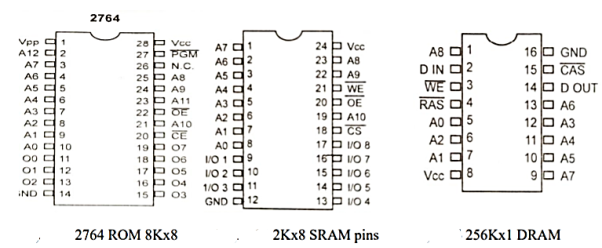
Memory Address Decoding
The job of the decoding circuitry to locate the selected memory block that CPU has access to desired data in memory chip. Memory chips have one more pins called CS (chip select) which must be activated for the memory contents to be accessed. Sometimes the chip select is also referred to as Chip Enable (CE). Following points are required for interfacing the memory to the CPU.
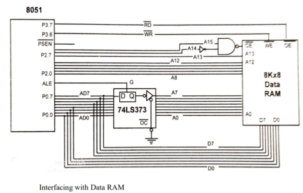
1. The data bus of the CPU is connected directly to data pins of the memory chip.
2. Control signals RD (read) and WR write from the CPU are connected to the OE (output enable) and WE (write enable) pins of memory chips respectively.
3. In case of the address buses, while lower bits of the addresses from the CPU are connected directly to the address pins of the memory chips and upper address pins are used to activate the CS or CE pin of the memory chip. The CS or CE pin along with RD/WR allows the flow of data in or out of the memory chip.
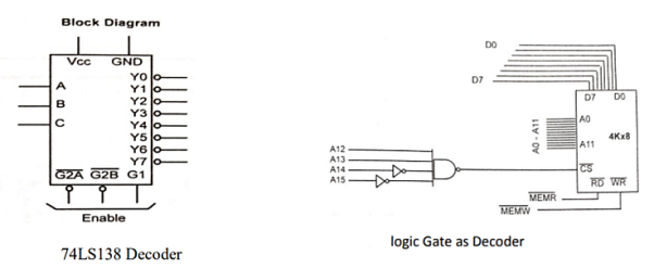
Interfacing with External ROM/RAM as Program and Data Memory
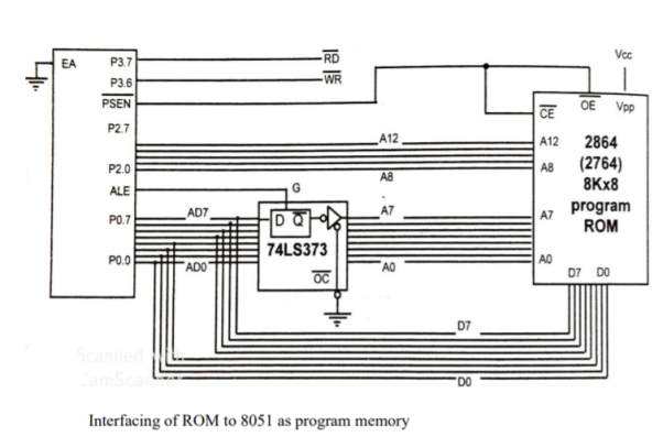
For interfacing to external ROM some pins have important role that to be discussed here. EA-When this pin is connected to Vcc, that indicates the program code is stored in the microcontroller on-chip ROM. For external ROM access tis pin is grounded.
P0 and P2 role in providing addresses- In 8051 P0 and P2 provides the 16-bit address to access external memory. Of these ports P0 provides the lower 8 bit addresses A0-A7, and P2 provides the upper 8 bit addresses A8-A15. More importantly, P0 is also used to provide 8 bit- data bus D0-D7. In other words P0.0- P0.7 are used for both address and Data is called as address/data multiplexing. The sharing of this bus is accomplished by ALE (address latch enable.) Pin. When ALE=0, the 8051 uses P0 for the data path and when ALE=1, it is used for address path.
 (program store enable)- It is an output signal must be connected to OE pin of a ROM containing the program code. When
  pin is connected to ground the 8051 fetches opcode from external ROM by using
  .
.

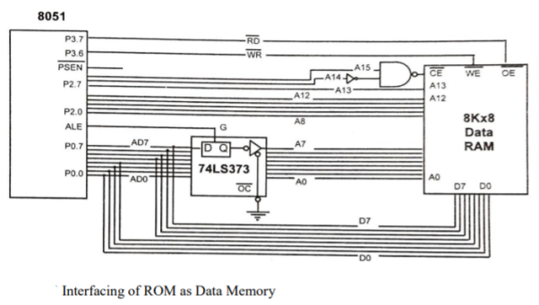

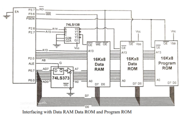
Pin Configuration

Fig 1: Pin Configuration of 8255
- It is also known as Programmable Peripheral Interface.
- It is a multi port device.
- It has 24 I/O pins. They are divided into three 8 bit ports PA, PB, PC.
- Port A and port B are used as 8-bit I/O ports.
- Port C is used as an 8-bit I/O port or as two 4-bit I/O ports or produces handshake signals for ports A and B.
- CS: The chip select CS (pin 6) is used to enable the 8255 chip. It is an active-low signal, hence is enabled when CS = 0.
- RESET: It is an input pin 35 and is connected to the RESET line of system 8085. When the system is reset, all the ports behave as input lines. This is done to prevent 8255 from being destroyed due to mismatch of ports.
- Eight data lines (D0–D7) are available to read/write data into the ports or control register under the status of the RD (pin 5) and WR (pin 36), which are active-low signals for read and write operations respectively.
- Address lines A1 and A0 allow to access a data register for each port or a control register, as listed below:
A1 | A0 | PORT SELECTED |
0 | 0 | PORT A |
0 | 1 | PORT B |
1 | 0 | PORT C |
1 | 1 | Control Register |
Operating Modes
There are two basic operating modes of 8255.
- Bit set/reset mode (BSR mode)
- Input/ output mode (I/O mode)
The modes selected by the D7 bit of the control word register are:
When D7 = 1, 8255 operates in I/O mode else BSR mode.
BSR MODE
The Bit Set/Reset (BSR) mode is available on port C only. Each and every line of port C (PC7 - PC0) can be set or reset by providing a suitable value to the control word register. BSR mode is independent and its selection does not affect the operation of other ports in I/O mode.

- D7 bit is always 0 for this mode.
- Bits D6, D5 and D4 are don't care bits.
- Bits D3, D2 and D1 are used for pin selection of Port C.
- Bit D0 is used to set/reset the above selected pin.
Selection of port C pin is determined as follows:
D3 | D2 | D1 | Bit/pin of port C selected |
0 | 0 | 0 | PC0 |
0 | 0 | 1 | PC1 |
0 | 1 | 0 | PC2 |
0 | 1 | 1 | PC3 |
1 | 0 | 0 | PC4 |
1 | 0 | 1 | PC5 |
1 | 1 | 0 | PC6 |
1 | 1 | 1 | PC7 |
For example:
If PC4 be set, then in the control word is,
- Since it is a BSR mode, D7 = '0'.
- Since D4, D5, D6 are don’t care hence assuming them to be '0'.
- PC4 has to be selected, hence, D3 = '1', D2 = '0', D1 = '0'.
- PC4 has to be set, hence, D0 = '1'.
Thus, as per the above values, 0AH (in hex) will be loaded into the Control Word Register (CWR).
I/O MODE
When D7 bit of the Control Word Register is 1, this mode is selected.
There are three I/O modes and they are:
- Mode 0 - Simple I/O
- Mode 1 - Strobed I/O
- Mode 2 - Strobed Bi-directional I/O
- Mode 0 – Simple or basic I/O mode:
Port A, B and C can work either as input or as output function. The outputs are latched but the inputs are not latched. It can handle interrupts.
- Mode 1 – Handshake or strobbed I/O:
Here, either port A or B can work and port C is used to provide handshake signals. The outputs as well as inputs are latched. It can handle interrupts. Before actual data is transmitted, there is transmission of signal to match speed of CPU and printer.
- Mode 2 – Bidirectional I/O:
In this mode only port A will work, port B can either is in mode 0 or 1 and port C bits are used as handshake signal. The outputs as well as inputs are latched. It has interrupt handling capability.
Functional block diagram
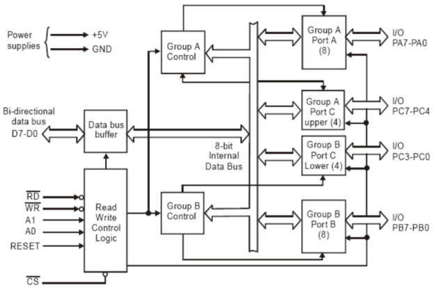
Fig 2. Functional Block Diagram
Control Word for I/O mode

- The most significant bit (D7) is 1 for the I/O mode.
- D6 & D5: It is used to set the port A mode.

- D4: It is used to check whether port A is taking input or displaying the output. If it is 1 then input else output.
- D3: It is used to check whether port C higher bites takes input or output. If 1, then input else output.
- D2: It tells the mode of port B. If 0, then port B is in M0 mode else in M1 mode.
- D1: It is used to check whether port B is taking input or displaying output. If 1, then input else output.
- D0: It is used to tell whether port C lower bits is taking input or displaying output. If 1, then it takes input else displays output.
I/O Port Expansion Using 8255
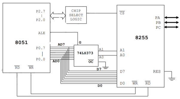
As seen earlier, for external memory interfacing to 8051 port 0 & port 2 are used as multiplexed address/data bus & higher order data bus respectively. If circuit needs on-chip peripherals (e.g. Serial I/O & interrupts) then only port is available for I/O. In such situation, I/O expansions is necessary & it is achieved by using 8255. Data bus of 8255 is connected to the port 0. Address line A0 & A1, after latches are connected to A0 & A1 of the 8255.
Keypad is used as an input device to read the key pressed by user and to process it.
4x4 keypad consists of 4 rows and 4 columns. Switches are placed between the rows and columns. A key press establishes a connection between corresponding row and column between which the switch is placed.
In order to read the keys press we need to configure the rows as outputs and columns as inputs.
Columns are read after applying signals to the rows in order to determine whether a key is pressed or not and if pressed, which key is pressed.

Figure 3. Keyboard matrix.

Figure 4. Keyboard Interfacing
#include <pic18f4550.h>
#include "Configuration_Header_File.h"
#include "16x2_LCD_4bit_File.h"
Unsigned char keyfind(); /* function to find pressed key */
#define write_port LATB /* latch register to write data on port */
#define read_port PORTB /* PORT register to read data of port */
#define Direction_Port TRISB
Unsigned char col_loc,rowloc,temp_col;
Unsigned char keypad[4][4]= {'7','8','9','/',
'4','5','6','*',
'1','2','3','-',
' ','0','=','+'};
Void main()
{
Char key;
OSCCON = 0x72;
RBPU=0; /* activate pull-up resistor */
LCD_Init(); /* initialize LCD16x2 in 4-bit mode */
LCD_String_xy(0,0,"Press a Key");
LCD_Command(0xC0); /* display pressed key on 2nd line of LCD */
While(1)
{
Key = keyfind(); /* find a pressed key */
LCD_Char(key); /* display pressed key on LCD16x2 */
}
}
Unsigned char keyfind()
{
Direction_Port = 0xf0; /* PORTD.0-PORTD.3 as a Output Port and PORTD.4-PORTD.7 as a Input Port*/
Unsigned char temp1;
Write_port = 0xf0; /* Make lower nibble as low(Gnd) and Higher nibble as High(Vcc) */
Do
{
Do
{
Col_loc = read_port & 0xf0; /* mask port with f0 and copy it to col_loc variable */
}while(col_loc!=0xf0); /* Check initially at the start there is any key pressed*/
Col_loc = read_port & 0xf0; /* mask port with f0 and copy it to col_loc variable */
}while(col_loc!=0xf0);
MSdelay(50);
Write_port = 0xf0; /* Make lower nibble as low(Gnd) and Higher nibble as High(Vcc) */
Do
{ do
{
Col_loc = read_port & 0xf0;
}while(col_loc==0xf0); /* Wait for key press */
Col_loc = read_port & 0xf0;
}while(col_loc==0xf0); /* Wait for key press */
MSdelay(20);
Col_loc = read_port & 0xf0;
While(1)
{
Write_port = 0xfe; /* make Row0(D0) Gnd and keep other row(D1-D3) high */
Col_loc = read_port & 0xf0; /* Read Status of PORT for finding Row */
Temp_col=col_loc;
If(col_loc!=0xf0)
{
Rowloc=0; /* If condition satisfied get Row no. Of key pressed */
While(temp_col!=0xf0) /* Monitor the status of Port and Wait for key to release */
{
Temp_col = read_port & 0xf0; /* Read Status of PORT for checking key release or not */
}
Break;
}
Write_port = 0xfd; /* make Row1(D1) Gnd and keep other row(D0-D2-D3) high */
Col_loc = read_port & 0xf0; /* Read Status of PORT for finding Row */
Temp_col=col_loc;
If(col_loc!=0xf0)
{
Rowloc=1; /* If condition satisfied get Row no. Of key pressed*/
While(temp_col!=0xf0) /* Monitor the status of Port and Wait for key to release */
{
Temp_col = read_port & 0xf0; /* Read Status of PORT for checking key release or not */
}
Break;
}
Write_port = 0xfb; /* make Row0(D2) Gnd and keep other row(D0-D1-D3) high */
Col_loc = read_port & 0xf0; /* Read Status of PORT for finding Row*/
Temp_col=col_loc;
If(col_loc!=0xf0)
{
Rowloc=2; /* If condition satisfied get Row no. Of key pressed */
While(temp_col!=0xf0) /* Wait for key to release */
{
Temp_col = read_port & 0xf0; /* Read Status of PORT for checking key release or not */
}
Break;
}
Write_port = 0xf7; /* make Row0(D3) Gnd and keep other row(D0-D2) high */
Col_loc = read_port & 0xf0; /* Read Status of PORT for finding Row */
Temp_col=col_loc;
If(col_loc!=0xf0)
{
Rowloc=3; /* If condition satisfied get Row no. Of key pressed */
While(temp_col!=0xf0) /* Wait for key to release */
{
Temp_col = read_port & 0xf0; /* Read Status of PORT for checking key release or not */
}
Break;
}
}
While(1)
{
If(col_loc==0xe0)
{
Return keypad[rowloc][0]; /* Return key pressed value to calling function */
}
Else
If(col_loc==0xd0)
{
Return keypad[rowloc][1]; /* Return key pressed value to calling function */
}
Else
If(col_loc==0xb0)
{
Return keypad[rowloc][2]; /* Return key pressed value to calling function */
}
Else
{
Return keypad[rowloc][3]; /* Return key pressed value to calling function */
}
}
MSdelay(300);
}
Light Emitting Diodes are considered as semi- conductor light sources. The commonly used LEDs have a cut-off voltage of 1.7V and current of 10mA. When applied with its required voltage and current it glows with full intensity.
The Light Emitting Diode works similar to normal PN- diode but it emits energy in the form of light. The colour of the light depends on the semiconductors band gap.

LED is connected to AT89C51 microcontroller with the current limiting resistor. The value of this resistor is calculated using the following formula.
R= (V-1.7)/10mA, where V is the input voltage.
The maximum output voltage of microcontrollers is 5V. Hence the calculated value of resistor is 330 Ohms. The resistor can be connected to cathode or the anode of LED.
- Initially, burn the code into the microcontroller.
- Connect the LEDs to the Port0 of the microcontroller.
- Switch on the circuit.
- The LEDs start glowing.
- Switch off the circuit.

LED Interfacing
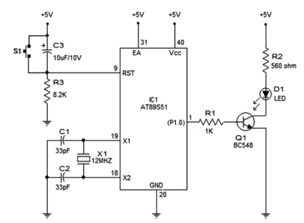
- In the circuit, push button switch S1, capacitor C3 and resistor R3 forms the reset circuitry.
- When S1 is pressed, voltage at the reset pin (pin9) goes high and this resets the chip. C1, C2 and X1 are related to the on -chip oscillator to produces the required clock frequency.
- P1.0 (pin1) is acts as the output pin. When P1.0turns high transistor Q1 is forward biased and LED gets ON. When P1.0 turns low, the transistor gets cut off and the LED extinguishes.
- The transistor driver circuit for the LED can be avoided and the LED can be connected directly to the P1.0 pinalong withthe series current limiting resistor(~1K).
- The time for which P1.0turns high and low (time period of the LED) is determined by the program.
Program:
START: CPL P1.0
ACALL WAIT
SJMP START
WAIT: MOV R4,#05H
WAIT1: MOV R3,#00H
WAIT2: MOV R2,#00H
WAIT3: DJNZ R2,WAIT3
DJNZ R3,WAIT2
DJNZ R4,WAIT1
RET
ADC0808/0809
ADC0808/0809 is a monolithic CMOS device which consists of 28 pin and gives 8-bit value in output for 8- channel ADC input pins (IN0-IN7).
It has resolution of 8 therefore it can encode the analog data into one of the 256 levels (28).
It has three channel address line namely: ADDA, ADDB and ADDC to select channel.
Pin Diagram for ADC0808
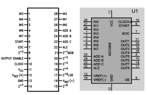
Figure 5. ADC 0808 Pin
ADC0808/0809 needs clock pulse for conversion which can be provided by using oscillator or microcontroller.
Select the input channel using address lines, like the input line IN0 by keeping all three address lines (ADDA, ADDB,ADDC) low.
Suppose IN2 is selected the keep ADDA and ADDB low and ADDC high.

Figure 6. Channel selection
SOC [Start of conversion]:
When High to low signal is appears on the pin of ADC, and ADC starts conversion

Figure 7. SOC
EOC [End of conversion]:
To indicate completion of conversion ADC sends high EOC signal to microcontroller.
OE [Output Enable]:
When a high signal is applied to this pin, the output latch of ADC is enabled and the converted data is made available to Microcontroller.
The reference voltage determines the range of analog input voltage.
For example: - If reference voltage is 5V then analog voltage ranges from 0V-5V.
If the reference voltage is 2.56V then the range is from 0V-2.56V.
The frequency of the applied clock signal determines conversion speed.
Working:
- Initially, microcontroller provides a 500 KHz clock signal to ADC0808 because the Timer 0 interrupt requires clock signal to operate to operate as ADC.
- Then the microcontroller sends a LOW to HIGH level signal to ALE pin (active-high pin) of ADC0808 to enable the latch in the address.
- By applying HIGH to LOW Level signal to SC (Start Conversion), ADC starts analog to digital conversion. And then wait for the EOC (End of Conversion) pin to go LOW.
- When EOC goes LOW, it means analog to digital conversion has been completed and data is ready to use.
- After this, microcontroller enables the output line by applying a HIGH to LOW signal to OE pin of ADC0808.
- ADC0808 gives ratio metric conversion output at its output pins.
Radiometric conversion is given by
Vin/(Vfs – Vz) = Dx / (Dmax – Dmin)
Where:
Vin is input voltage for conversion
Vfs is full scale voltage
Vz is zero voltage
Dx is data point being measured
Dmax is maximum data limit
Dmin is minimum data limit.
Interfacing Diagram:
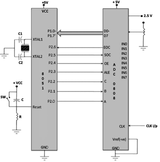
Figure 8. Interfacing 8051 with ADC0808
Program:
SOC EQU P2.6
EOC EQU P2.5
OE EQU P2.4
ALE EQU P2.3
ADDR_C EQU P2.2
ADDR_B EQU P2.1
ADDR_A EQU P2.0
ORG 0000H
MOV P1, #0FFH
SETB P2.5
CLR SOC
CLR OE
CLR ALE
AGAIN: CLR ADDR_C
CLR ADDR_B
CLR ADDR_A
SETB SOC
SET ALE
ACALL DELAY
CLR SOC
CLR ALE
BACK: JB EOC BACK
HERE: JNB EOC HERE
SETB OE
MOV A,P1
ACALL CONVERSION
ACALL DISPLAY
AGAIN: SJMP AGAIN
Key takeaway
ADC0808/0809 needs clock pulse for conversion which can be provided by using oscillator or microcontroller.
SOC- When High to low signal is appears on the pin of ADC, andADC starts conversion
EOC- To indicate completion of conversion ADC sends high EOC signal to microcontroller.
DAC (0808)
In these systems the microcontroller generates output in digital form, The controlling system requires analog signal because they don't accept digital data. Hence, there is a need to use DAC which converts digital data into its equivalent analog voltage.
In the figure shown, we use 8-bit DAC 0808. This IC converts digital data into its equivalent analog current. The I to V converter converts the current into its equivalent voltage.
According to theory of DAC Equivalent analog output is given as:

Ex:
1. IF data =00H [00000000] and
Vref = 10V

Therefore, V0= 0 Volts.
2. If data is 80H [10000000],
And Vref = 10V

Therefore, V0= 5 Volts.
Different Analog output voltages for different Digital signal is given as:
DATA | OUTPUT VOLTAGE |
00H | 0V |
80H | 5V |
FFH | 10V |
Interfacing Diagram
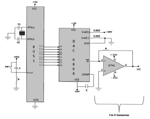
Figure 9. Interfacing 8051 with DAC 0808
Program:
ORG 000H
MOV P1, #00H
Call squarwave
Call triwave
Call stairwave
Jmp repeat
Squarwave: MOV P1,#FFH
Call delay2sec
MOV P1,#00H
Call delay2sec
Ret
Triwave: MOV R7,#00H
Triwave1: MOV P1,R7
Inc R7
Cjne R7, #FFH, triwave1
MOV R7, #FFh
Triwave2: MOV P1, R7
Djnz R7, triwave2
RET
Stairwave: MOV P1, #00H
Call delay2sec
MOV P1, #20H
Call delay2sec
MOV P1, #40H
Call delay2sec
RET
Delay1sec: MOV R0,#10
Del2 : MOV R1,#250
Del1: MOV R2,#250
DJNZ R2,$
DJNZ R1,del2
DJNZ R0,del1
RET
Delay2sec: MOV R0,#20
Del2 : MOV R1,#250
Del1: MOV R2,#250
DJNZ R2,$
DJNZ R1,del21
DJNZ R0,del22
RET
END
Key takeaway
In these systems the microcontroller generates output in digital form, The controlling system requires analog signal because they don't accept digital data. Hence, there is a need to use DAC which converts digital data into its equivalent analog voltage.
Stepper motors is mainly used to translate electrical pulses into mechanical movements.
They are used in some disk drives, dot matrix printers. The key advantage of using stepper motor is its position control.
Stepper motors generally have a permanent magnet shaft (rotor), and it is surrounded by a stator.

Figure 10: Stepper Motor
Parameters of stepper motors:
Step Angle - The step angle is the angle at which the rotor moves when one pulse is applied as an input to the stator. This parameter determines the position of stepper motor.
Steps per Revolution - This is the number of step angles required for a complete revolution. The formula is 360° /Step Angle.
Steps per Second - This parameter is used to measure number of steps covered in each second.
RPM - The RPM is the Revolution Per Minute. It measures the frequency of rotation. We can measure the number of rotations in one minute.
The relation between RPM steps per revolution and steps per second is
Steps per second = rpm x steps per revolution / 60
Interfacing
Port P0 of 8051 is used for connecting the stepper motor. HereULN2003 is used. This is basically a high voltage, high current Darlington transistor array. Each ULN2003 has seven NPN Darlington pairs. It can provide high voltage output with common cathode clamp diodes for switching inductive loads.
The Unipolar stepper motor works in three modes.
Wave Drive Mode: In this mode, one coil is energized at a time. So all four coils are energized one after another. This mode produces less torque than full step drive mode.
Steps | Winding A | Winding B | Winding C | Winding D |
1 | 1 | 0 | 0 | 0 |
2 | 0 | 1 | 0 | 0 |
3 | 0 | 0 | 1 | 0 |
4 | 0 | 0 | 0 | 1 |
Full Drive Mode: In this mode, two coils are energized at the same time. This mode produces more torque. Here the power consumption is also high.
Steps | Winding A | Winding B | Winding C | Winding D |
1 | 1 | 1 | 0 | 0 |
2 | 0 | 1 | 1 | 0 |
3 | 0 | 0 | 1 | 1 |
4 | 1 | 0 | 0 | 1 |
Half Drive Mode: In this mode, one and two coils are energized alternately. At first, one coil is energized then two coils are energized. This is basically a combination of wave and full drive mode. It increases the angular rotation of the motor.
Steps | Winding A | Winding B | Winding C | Winding D |
1 | 1 | 0 | 0 | 0 |
2 | 1 | 1 | 0 | 0 |
3 | 0 | 1 | 0 | 0 |
4 | 0 | 1 | 1 | 0 |
5 | 0 | 0 | 1 | 0 |
6 | 0 | 0 | 1 | 1 |
7 | 0 | 0 | 0 | 1 |
8 | 1 | 0 | 0 | 1 |
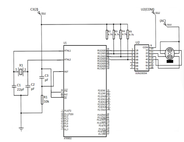
Figure 11. Interfacing Stepper Motor with 8051
Program:
Main: MOV A, # 0FF H ; Initialization of Port 1
MOV P1, A ;
MOV A, #77 H ; Code for the Phase 1
MOV P1, A ; ACALL DELAY ; Delay subroutine
MOV A, # BB H ; Code for the Phase II
MOV P1, A ;
ACALL DELAY ; Delay subroutine.
MOV A, # DD H ; Code for the Phase III
MOV P1, A ; ACALL DELAY ;
MOV A, # EE H ; Code for the Phase 1
MOV P1, A ;
ACALL DELAY ; Delay subroutine
SJMP MAIN; Keep the motor rotating continuously.
DELAY Subroutine
MOV R4, #0FF H ; Load R4 with FF
MOV R5, # 0FF ; Load R5 with FF
LOOP1: DJNZ R4, LOOP1 ; Decrement R4 until zero,wait
LOOP2: DJNZ R5, LOOP2 ; Decrement R5 until zero,wait
RET ; Return to main program .
Key takeaway
Stepper motors is mainly used to translate electrical pulses into mechanical movements.
They are used in some disk drives, dot matrix printers. The key advantage of using stepper motor is its position control.
References:
1. M. A.Mazidi, J. G. Mazidi and R. D. McKinlay, “The8051Microcontroller and Embedded Systems: Using Assembly and C”, Pearson Education, 2007.
2. K. J. Ayala, “8051 Microcontroller”, Delmar Cengage Learning,2004.
3. The 8051 Microcontroller Based Embedded System By Manish K. Patel TMH.
4. Embedded System Architecture, Programming and Design by Raj Kamal, 3rd Edition TMH.
5. Introduction to Embedded System by Shibu K. V. 3rd Edition TMH
Unit - 3
Memory and I/O Interfacing
Unit - 3
Memory and I/O Interfacing
In the design of all microprocessor-based system, Semiconductor memory are used as primary storage for code and data. It can be in units of K bits, M bits and so on. Semiconductor memories are conducted directly to the CPU and is also called as primary memory. The widely used semiconductor memories are ROM and RAM.
Characteristics of Semiconductor Memory
Memory capacity- The number of bits that a semiconductor memory chip can store is called chip capacity
Memory organization- Memory chips are organized into number of locations within the IC. Each location holds 1 bit, 4bits, 8bits or even 16 bits, depending on how it is designed internally.
1. A memory chip contains 2x locations where x is the number of address pins.
2. Each location contains y bits, where y is the number of data pins on the chip.
3. The entire chip will contain 2x x y bits, where x is the number of address pins and y is the number of data pins.
Speed- One of the most important characteristics of a memory chip is the speed at which its data can be accessed.
ROM (Read-Only-Memory)- It is a type of memory that does not loss its contents when the power is turned off. For this reason ROM is called volatile memory. There are different types of read-only- memory such as PROM, EPROM, EEPROM, Flash EPROM and mask ROM.
PROM- It refers to the kind of ROM that the user can burn information into it. That’s why it is called as user-programmable memory. For every bit of the PROM, there exists a fuse. So it is programmed by blowing of fuses. It is also referred to as OTP (one –time programmable)
EPROM (Erasable Programmable ROM)- In EPROM, one can program the memory chip and erase it thousands of times. A widely used EPROM is called UV-EPROM. The content of UV-EPROM is erased when it is exposed to ultra violet light. Its erase time is near about 20 minutes.
EEPROM (Electrically Erasable Programmable ROM)- Its desired contents are erased by electrically.
Flash memory EPROM- This memory has become popular user-programmable memory chip, due to the process of erasure of the entire contents takes less than a second. As the erasure method is electrical sometimes it is called as Flash EEPROM.
Mask ROM- Mask ROM refers to kind of ROM in which the contents are programmed by the IC manufacturer. It is not a user-programmable ROM.
RAM (Random Access Memory)- It is called volatile memory since cutting of the power to the IC will result in the loss of data. Sometimes it is called as read and write memory (RAWM). There are three types of RAMs: Static RAM (SRAM), NV-RAM (Non-volatile RAM) and dynamic RAM (DRAM).
NV-RAM (Non-volatile RAM)-This RAM is non-volatile. Like other RAMs it allows the CPU to read write to it, but when the power is turned off, the contents are not lost. To retain its content every NV-RAM chip internally is made of the following components.
1. It uses extremely power-efficient. SRAM cells built out of CMOS
2. It uses an internal lithium battery as back energy source.
3. It uses an intelligent control circuitry. The main job of internal circuitry to monitor the Vcc pin constantly to detect the loss of external power supply. If the power to the Vcc pin falls the below out-of-tolerance condition, the control circuitry switches automatically to its internal power source, lithium battery.
DRAM (Dynamic RAM)-The use of a capacitor as a means to store data cuts down the number of transistors needed to build up the cell; however, it requires constant refreshing due to leakage. This is in contrast to SRAM whose cells are made of flip-lops. The use of capacitor as storage cells in DRAM results in much smaller net memory size.

Memory Address Decoding
The job of the decoding circuitry to locate the selected memory block that CPU has access to desired data in memory chip. Memory chips have one more pins called CS (chip select) which must be activated for the memory contents to be accessed. Sometimes the chip select is also referred to as Chip Enable (CE). Following points are required for interfacing the memory to the CPU.
1. The data bus of the CPU is connected directly to data pins of the memory chip.
2. Control signals RD (read) and WR write from the CPU are connected to the OE (output enable) and WE (write enable) pins of memory chips respectively.
3. In case of the address buses, while lower bits of the addresses from the CPU are connected directly to the address pins of the memory chips and upper address pins are used to activate the CS or CE pin of the memory chip. The CS or CE pin along with RD/WR allows the flow of data in or out of the memory chip.

Interfacing with External ROM/RAM as Program and Data Memory
For interfacing to external ROM some pins have important role that to be discussed here. EA-When this pin is connected to Vcc, that indicates the program code is stored in the microcontroller on-chip ROM. For external ROM access tis pin is grounded.
P0 and P2 role in providing addresses- In 8051 P0 and P2 provides the 16-bit address to access external memory. Of these ports P0 provides the lower 8 bit addresses A0-A7, and P2 provides the upper 8 bit addresses A8-A15. More importantly, P0 is also used to provide 8 bit- data bus D0-D7. In other words P0.0- P0.7 are used for both address and Data is called as address/data multiplexing. The sharing of this bus is accomplished by ALE (address latch enable.) Pin. When ALE=0, the 8051 uses P0 for the data path and when ALE=1, it is used for address path.
 (program store enable)- It is an output signal must be connected to OE pin of a ROM containing the program code. When
  pin is connected to ground the 8051 fetches opcode from external ROM by using
  .
.


Pin Configuration
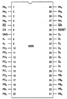
Fig 1: Pin Configuration of 8255
- It is also known as Programmable Peripheral Interface.
- It is a multi port device.
- It has 24 I/O pins. They are divided into three 8 bit ports PA, PB, PC.
- Port A and port B are used as 8-bit I/O ports.
- Port C is used as an 8-bit I/O port or as two 4-bit I/O ports or produces handshake signals for ports A and B.
- CS: The chip select CS (pin 6) is used to enable the 8255 chip. It is an active-low signal, hence is enabled when CS = 0.
- RESET: It is an input pin 35 and is connected to the RESET line of system 8085. When the system is reset, all the ports behave as input lines. This is done to prevent 8255 from being destroyed due to mismatch of ports.
- Eight data lines (D0–D7) are available to read/write data into the ports or control register under the status of the RD (pin 5) and WR (pin 36), which are active-low signals for read and write operations respectively.
- Address lines A1 and A0 allow to access a data register for each port or a control register, as listed below:
A1 | A0 | PORT SELECTED |
0 | 0 | PORT A |
0 | 1 | PORT B |
1 | 0 | PORT C |
1 | 1 | Control Register |
Operating Modes
There are two basic operating modes of 8255.
- Bit set/reset mode (BSR mode)
- Input/ output mode (I/O mode)
The modes selected by the D7 bit of the control word register are:
When D7 = 1, 8255 operates in I/O mode else BSR mode.
BSR MODE
The Bit Set/Reset (BSR) mode is available on port C only. Each and every line of port C (PC7 - PC0) can be set or reset by providing a suitable value to the control word register. BSR mode is independent and its selection does not affect the operation of other ports in I/O mode.

- D7 bit is always 0 for this mode.
- Bits D6, D5 and D4 are don't care bits.
- Bits D3, D2 and D1 are used for pin selection of Port C.
- Bit D0 is used to set/reset the above selected pin.
Selection of port C pin is determined as follows:
D3 | D2 | D1 | Bit/pin of port C selected |
0 | 0 | 0 | PC0 |
0 | 0 | 1 | PC1 |
0 | 1 | 0 | PC2 |
0 | 1 | 1 | PC3 |
1 | 0 | 0 | PC4 |
1 | 0 | 1 | PC5 |
1 | 1 | 0 | PC6 |
1 | 1 | 1 | PC7 |
For example:
If PC4 be set, then in the control word is,
- Since it is a BSR mode, D7 = '0'.
- Since D4, D5, D6 are don’t care hence assuming them to be '0'.
- PC4 has to be selected, hence, D3 = '1', D2 = '0', D1 = '0'.
- PC4 has to be set, hence, D0 = '1'.
Thus, as per the above values, 0AH (in hex) will be loaded into the Control Word Register (CWR).
I/O MODE
When D7 bit of the Control Word Register is 1, this mode is selected.
There are three I/O modes and they are:
- Mode 0 - Simple I/O
- Mode 1 - Strobed I/O
- Mode 2 - Strobed Bi-directional I/O
- Mode 0 – Simple or basic I/O mode:
Port A, B and C can work either as input or as output function. The outputs are latched but the inputs are not latched. It can handle interrupts.
- Mode 1 – Handshake or strobbed I/O:
Here, either port A or B can work and port C is used to provide handshake signals. The outputs as well as inputs are latched. It can handle interrupts. Before actual data is transmitted, there is transmission of signal to match speed of CPU and printer.
- Mode 2 – Bidirectional I/O:
In this mode only port A will work, port B can either is in mode 0 or 1 and port C bits are used as handshake signal. The outputs as well as inputs are latched. It has interrupt handling capability.
Functional block diagram

Fig 2. Functional Block Diagram
Control Word for I/O mode
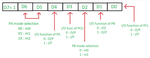
- The most significant bit (D7) is 1 for the I/O mode.
- D6 & D5: It is used to set the port A mode.

- D4: It is used to check whether port A is taking input or displaying the output. If it is 1 then input else output.
- D3: It is used to check whether port C higher bites takes input or output. If 1, then input else output.
- D2: It tells the mode of port B. If 0, then port B is in M0 mode else in M1 mode.
- D1: It is used to check whether port B is taking input or displaying output. If 1, then input else output.
- D0: It is used to tell whether port C lower bits is taking input or displaying output. If 1, then it takes input else displays output.
I/O Port Expansion Using 8255

As seen earlier, for external memory interfacing to 8051 port 0 & port 2 are used as multiplexed address/data bus & higher order data bus respectively. If circuit needs on-chip peripherals (e.g. Serial I/O & interrupts) then only port is available for I/O. In such situation, I/O expansions is necessary & it is achieved by using 8255. Data bus of 8255 is connected to the port 0. Address line A0 & A1, after latches are connected to A0 & A1 of the 8255.
Keypad is used as an input device to read the key pressed by user and to process it.
4x4 keypad consists of 4 rows and 4 columns. Switches are placed between the rows and columns. A key press establishes a connection between corresponding row and column between which the switch is placed.
In order to read the keys press we need to configure the rows as outputs and columns as inputs.
Columns are read after applying signals to the rows in order to determine whether a key is pressed or not and if pressed, which key is pressed.
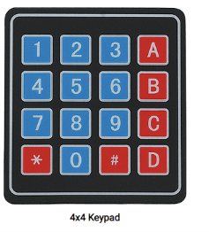
Figure 3. Keyboard matrix.
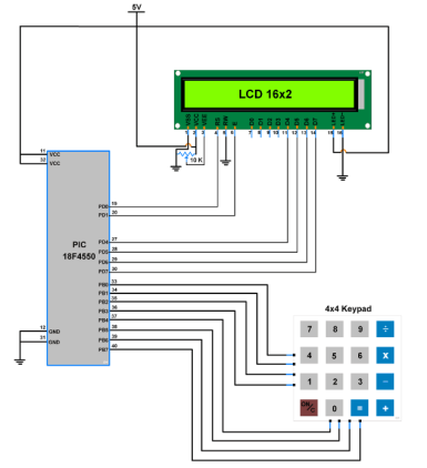
Figure 4. Keyboard Interfacing
#include <pic18f4550.h>
#include "Configuration_Header_File.h"
#include "16x2_LCD_4bit_File.h"
Unsigned char keyfind(); /* function to find pressed key */
#define write_port LATB /* latch register to write data on port */
#define read_port PORTB /* PORT register to read data of port */
#define Direction_Port TRISB
Unsigned char col_loc,rowloc,temp_col;
Unsigned char keypad[4][4]= {'7','8','9','/',
'4','5','6','*',
'1','2','3','-',
' ','0','=','+'};
Void main()
{
Char key;
OSCCON = 0x72;
RBPU=0; /* activate pull-up resistor */
LCD_Init(); /* initialize LCD16x2 in 4-bit mode */
LCD_String_xy(0,0,"Press a Key");
LCD_Command(0xC0); /* display pressed key on 2nd line of LCD */
While(1)
{
Key = keyfind(); /* find a pressed key */
LCD_Char(key); /* display pressed key on LCD16x2 */
}
}
Unsigned char keyfind()
{
Direction_Port = 0xf0; /* PORTD.0-PORTD.3 as a Output Port and PORTD.4-PORTD.7 as a Input Port*/
Unsigned char temp1;
Write_port = 0xf0; /* Make lower nibble as low(Gnd) and Higher nibble as High(Vcc) */
Do
{
Do
{
Col_loc = read_port & 0xf0; /* mask port with f0 and copy it to col_loc variable */
}while(col_loc!=0xf0); /* Check initially at the start there is any key pressed*/
Col_loc = read_port & 0xf0; /* mask port with f0 and copy it to col_loc variable */
}while(col_loc!=0xf0);
MSdelay(50);
Write_port = 0xf0; /* Make lower nibble as low(Gnd) and Higher nibble as High(Vcc) */
Do
{ do
{
Col_loc = read_port & 0xf0;
}while(col_loc==0xf0); /* Wait for key press */
Col_loc = read_port & 0xf0;
}while(col_loc==0xf0); /* Wait for key press */
MSdelay(20);
Col_loc = read_port & 0xf0;
While(1)
{
Write_port = 0xfe; /* make Row0(D0) Gnd and keep other row(D1-D3) high */
Col_loc = read_port & 0xf0; /* Read Status of PORT for finding Row */
Temp_col=col_loc;
If(col_loc!=0xf0)
{
Rowloc=0; /* If condition satisfied get Row no. Of key pressed */
While(temp_col!=0xf0) /* Monitor the status of Port and Wait for key to release */
{
Temp_col = read_port & 0xf0; /* Read Status of PORT for checking key release or not */
}
Break;
}
Write_port = 0xfd; /* make Row1(D1) Gnd and keep other row(D0-D2-D3) high */
Col_loc = read_port & 0xf0; /* Read Status of PORT for finding Row */
Temp_col=col_loc;
If(col_loc!=0xf0)
{
Rowloc=1; /* If condition satisfied get Row no. Of key pressed*/
While(temp_col!=0xf0) /* Monitor the status of Port and Wait for key to release */
{
Temp_col = read_port & 0xf0; /* Read Status of PORT for checking key release or not */
}
Break;
}
Write_port = 0xfb; /* make Row0(D2) Gnd and keep other row(D0-D1-D3) high */
Col_loc = read_port & 0xf0; /* Read Status of PORT for finding Row*/
Temp_col=col_loc;
If(col_loc!=0xf0)
{
Rowloc=2; /* If condition satisfied get Row no. Of key pressed */
While(temp_col!=0xf0) /* Wait for key to release */
{
Temp_col = read_port & 0xf0; /* Read Status of PORT for checking key release or not */
}
Break;
}
Write_port = 0xf7; /* make Row0(D3) Gnd and keep other row(D0-D2) high */
Col_loc = read_port & 0xf0; /* Read Status of PORT for finding Row */
Temp_col=col_loc;
If(col_loc!=0xf0)
{
Rowloc=3; /* If condition satisfied get Row no. Of key pressed */
While(temp_col!=0xf0) /* Wait for key to release */
{
Temp_col = read_port & 0xf0; /* Read Status of PORT for checking key release or not */
}
Break;
}
}
While(1)
{
If(col_loc==0xe0)
{
Return keypad[rowloc][0]; /* Return key pressed value to calling function */
}
Else
If(col_loc==0xd0)
{
Return keypad[rowloc][1]; /* Return key pressed value to calling function */
}
Else
If(col_loc==0xb0)
{
Return keypad[rowloc][2]; /* Return key pressed value to calling function */
}
Else
{
Return keypad[rowloc][3]; /* Return key pressed value to calling function */
}
}
MSdelay(300);
}
Light Emitting Diodes are considered as semi- conductor light sources. The commonly used LEDs have a cut-off voltage of 1.7V and current of 10mA. When applied with its required voltage and current it glows with full intensity.
The Light Emitting Diode works similar to normal PN- diode but it emits energy in the form of light. The colour of the light depends on the semiconductors band gap.

LED is connected to AT89C51 microcontroller with the current limiting resistor. The value of this resistor is calculated using the following formula.
R= (V-1.7)/10mA, where V is the input voltage.
The maximum output voltage of microcontrollers is 5V. Hence the calculated value of resistor is 330 Ohms. The resistor can be connected to cathode or the anode of LED.
- Initially, burn the code into the microcontroller.
- Connect the LEDs to the Port0 of the microcontroller.
- Switch on the circuit.
- The LEDs start glowing.
- Switch off the circuit.
LED Interfacing
- In the circuit, push button switch S1, capacitor C3 and resistor R3 forms the reset circuitry.
- When S1 is pressed, voltage at the reset pin (pin9) goes high and this resets the chip. C1, C2 and X1 are related to the on -chip oscillator to produces the required clock frequency.
- P1.0 (pin1) is acts as the output pin. When P1.0turns high transistor Q1 is forward biased and LED gets ON. When P1.0 turns low, the transistor gets cut off and the LED extinguishes.
- The transistor driver circuit for the LED can be avoided and the LED can be connected directly to the P1.0 pinalong withthe series current limiting resistor(~1K).
- The time for which P1.0turns high and low (time period of the LED) is determined by the program.
Program:
START: CPL P1.0
ACALL WAIT
SJMP START
WAIT: MOV R4,#05H
WAIT1: MOV R3,#00H
WAIT2: MOV R2,#00H
WAIT3: DJNZ R2,WAIT3
DJNZ R3,WAIT2
DJNZ R4,WAIT1
RET
ADC0808/0809
ADC0808/0809 is a monolithic CMOS device which consists of 28 pin and gives 8-bit value in output for 8- channel ADC input pins (IN0-IN7).
It has resolution of 8 therefore it can encode the analog data into one of the 256 levels (28).
It has three channel address line namely: ADDA, ADDB and ADDC to select channel.
Pin Diagram for ADC0808

Figure 5. ADC 0808 Pin
ADC0808/0809 needs clock pulse for conversion which can be provided by using oscillator or microcontroller.
Select the input channel using address lines, like the input line IN0 by keeping all three address lines (ADDA, ADDB,ADDC) low.
Suppose IN2 is selected the keep ADDA and ADDB low and ADDC high.
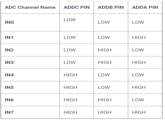
Figure 6. Channel selection
SOC [Start of conversion]:
When High to low signal is appears on the pin of ADC, and ADC starts conversion

Figure 7. SOC
EOC [End of conversion]:
To indicate completion of conversion ADC sends high EOC signal to microcontroller.
OE [Output Enable]:
When a high signal is applied to this pin, the output latch of ADC is enabled and the converted data is made available to Microcontroller.
The reference voltage determines the range of analog input voltage.
For example: - If reference voltage is 5V then analog voltage ranges from 0V-5V.
If the reference voltage is 2.56V then the range is from 0V-2.56V.
The frequency of the applied clock signal determines conversion speed.
Working:
- Initially, microcontroller provides a 500 KHz clock signal to ADC0808 because the Timer 0 interrupt requires clock signal to operate to operate as ADC.
- Then the microcontroller sends a LOW to HIGH level signal to ALE pin (active-high pin) of ADC0808 to enable the latch in the address.
- By applying HIGH to LOW Level signal to SC (Start Conversion), ADC starts analog to digital conversion. And then wait for the EOC (End of Conversion) pin to go LOW.
- When EOC goes LOW, it means analog to digital conversion has been completed and data is ready to use.
- After this, microcontroller enables the output line by applying a HIGH to LOW signal to OE pin of ADC0808.
- ADC0808 gives ratio metric conversion output at its output pins.
Radiometric conversion is given by
Vin/(Vfs – Vz) = Dx / (Dmax – Dmin)
Where:
Vin is input voltage for conversion
Vfs is full scale voltage
Vz is zero voltage
Dx is data point being measured
Dmax is maximum data limit
Dmin is minimum data limit.
Interfacing Diagram:

Figure 8. Interfacing 8051 with ADC0808
Program:
SOC EQU P2.6
EOC EQU P2.5
OE EQU P2.4
ALE EQU P2.3
ADDR_C EQU P2.2
ADDR_B EQU P2.1
ADDR_A EQU P2.0
ORG 0000H
MOV P1, #0FFH
SETB P2.5
CLR SOC
CLR OE
CLR ALE
AGAIN: CLR ADDR_C
CLR ADDR_B
CLR ADDR_A
SETB SOC
SET ALE
ACALL DELAY
CLR SOC
CLR ALE
BACK: JB EOC BACK
HERE: JNB EOC HERE
SETB OE
MOV A,P1
ACALL CONVERSION
ACALL DISPLAY
AGAIN: SJMP AGAIN
Key takeaway
ADC0808/0809 needs clock pulse for conversion which can be provided by using oscillator or microcontroller.
SOC- When High to low signal is appears on the pin of ADC, andADC starts conversion
EOC- To indicate completion of conversion ADC sends high EOC signal to microcontroller.
DAC (0808)
In these systems the microcontroller generates output in digital form, The controlling system requires analog signal because they don't accept digital data. Hence, there is a need to use DAC which converts digital data into its equivalent analog voltage.
In the figure shown, we use 8-bit DAC 0808. This IC converts digital data into its equivalent analog current. The I to V converter converts the current into its equivalent voltage.
According to theory of DAC Equivalent analog output is given as:

Ex:
1. IF data =00H [00000000] and
Vref = 10V

Therefore, V0= 0 Volts.
2. If data is 80H [10000000],
And Vref = 10V

Therefore, V0= 5 Volts.
Different Analog output voltages for different Digital signal is given as:
DATA | OUTPUT VOLTAGE |
00H | 0V |
80H | 5V |
FFH | 10V |
Interfacing Diagram

Figure 9. Interfacing 8051 with DAC 0808
Program:
ORG 000H
MOV P1, #00H
Call squarwave
Call triwave
Call stairwave
Jmp repeat
Squarwave: MOV P1,#FFH
Call delay2sec
MOV P1,#00H
Call delay2sec
Ret
Triwave: MOV R7,#00H
Triwave1: MOV P1,R7
Inc R7
Cjne R7, #FFH, triwave1
MOV R7, #FFh
Triwave2: MOV P1, R7
Djnz R7, triwave2
RET
Stairwave: MOV P1, #00H
Call delay2sec
MOV P1, #20H
Call delay2sec
MOV P1, #40H
Call delay2sec
RET
Delay1sec: MOV R0,#10
Del2 : MOV R1,#250
Del1: MOV R2,#250
DJNZ R2,$
DJNZ R1,del2
DJNZ R0,del1
RET
Delay2sec: MOV R0,#20
Del2 : MOV R1,#250
Del1: MOV R2,#250
DJNZ R2,$
DJNZ R1,del21
DJNZ R0,del22
RET
END
Key takeaway
In these systems the microcontroller generates output in digital form, The controlling system requires analog signal because they don't accept digital data. Hence, there is a need to use DAC which converts digital data into its equivalent analog voltage.
Stepper motors is mainly used to translate electrical pulses into mechanical movements.
They are used in some disk drives, dot matrix printers. The key advantage of using stepper motor is its position control.
Stepper motors generally have a permanent magnet shaft (rotor), and it is surrounded by a stator.
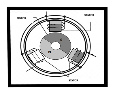
Figure 10: Stepper Motor
Parameters of stepper motors:
Step Angle - The step angle is the angle at which the rotor moves when one pulse is applied as an input to the stator. This parameter determines the position of stepper motor.
Steps per Revolution - This is the number of step angles required for a complete revolution. The formula is 360° /Step Angle.
Steps per Second - This parameter is used to measure number of steps covered in each second.
RPM - The RPM is the Revolution Per Minute. It measures the frequency of rotation. We can measure the number of rotations in one minute.
The relation between RPM steps per revolution and steps per second is
Steps per second = rpm x steps per revolution / 60
Interfacing
Port P0 of 8051 is used for connecting the stepper motor. HereULN2003 is used. This is basically a high voltage, high current Darlington transistor array. Each ULN2003 has seven NPN Darlington pairs. It can provide high voltage output with common cathode clamp diodes for switching inductive loads.
The Unipolar stepper motor works in three modes.
Wave Drive Mode: In this mode, one coil is energized at a time. So all four coils are energized one after another. This mode produces less torque than full step drive mode.
Steps | Winding A | Winding B | Winding C | Winding D |
1 | 1 | 0 | 0 | 0 |
2 | 0 | 1 | 0 | 0 |
3 | 0 | 0 | 1 | 0 |
4 | 0 | 0 | 0 | 1 |
Full Drive Mode: In this mode, two coils are energized at the same time. This mode produces more torque. Here the power consumption is also high.
Steps | Winding A | Winding B | Winding C | Winding D |
1 | 1 | 1 | 0 | 0 |
2 | 0 | 1 | 1 | 0 |
3 | 0 | 0 | 1 | 1 |
4 | 1 | 0 | 0 | 1 |
Half Drive Mode: In this mode, one and two coils are energized alternately. At first, one coil is energized then two coils are energized. This is basically a combination of wave and full drive mode. It increases the angular rotation of the motor.
Steps | Winding A | Winding B | Winding C | Winding D |
1 | 1 | 0 | 0 | 0 |
2 | 1 | 1 | 0 | 0 |
3 | 0 | 1 | 0 | 0 |
4 | 0 | 1 | 1 | 0 |
5 | 0 | 0 | 1 | 0 |
6 | 0 | 0 | 1 | 1 |
7 | 0 | 0 | 0 | 1 |
8 | 1 | 0 | 0 | 1 |

Figure 11. Interfacing Stepper Motor with 8051
Program:
Main: MOV A, # 0FF H ; Initialization of Port 1
MOV P1, A ;
MOV A, #77 H ; Code for the Phase 1
MOV P1, A ; ACALL DELAY ; Delay subroutine
MOV A, # BB H ; Code for the Phase II
MOV P1, A ;
ACALL DELAY ; Delay subroutine.
MOV A, # DD H ; Code for the Phase III
MOV P1, A ; ACALL DELAY ;
MOV A, # EE H ; Code for the Phase 1
MOV P1, A ;
ACALL DELAY ; Delay subroutine
SJMP MAIN; Keep the motor rotating continuously.
DELAY Subroutine
MOV R4, #0FF H ; Load R4 with FF
MOV R5, # 0FF ; Load R5 with FF
LOOP1: DJNZ R4, LOOP1 ; Decrement R4 until zero,wait
LOOP2: DJNZ R5, LOOP2 ; Decrement R5 until zero,wait
RET ; Return to main program .
Key takeaway
Stepper motors is mainly used to translate electrical pulses into mechanical movements.
They are used in some disk drives, dot matrix printers. The key advantage of using stepper motor is its position control.
References:
1. M. A.Mazidi, J. G. Mazidi and R. D. McKinlay, “The8051Microcontroller and Embedded Systems: Using Assembly and C”, Pearson Education, 2007.
2. K. J. Ayala, “8051 Microcontroller”, Delmar Cengage Learning,2004.
3. The 8051 Microcontroller Based Embedded System By Manish K. Patel TMH.
4. Embedded System Architecture, Programming and Design by Raj Kamal, 3rd Edition TMH.
5. Introduction to Embedded System by Shibu K. V. 3rd Edition TMH