Unit - 5
Devices and Communication
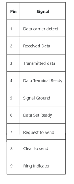
RS-232 represents serial data transmission. RS232 transmits signals using a positive voltage for binary 0 and negative voltage for binary 1.
To talk to other modules PLCs, use RS232. These modules may be anything that use RS232 as operator, interface or HMI, computers, motor controller’s robot or vision system.

Figure 1. DB-9 connector
RS-232 Line Driver
- It consists of two-line drivers, two-line receivers, and a dual charge-pump circuit with ±15 kV ESD protection.
- It provides the electrical interface between an asynchronous communication controller and a serial port connector.
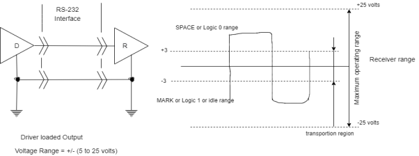
Figure 2. RS-232 Line Driver
- The maximum speed is 20kbit/s. However, modern equipment can operate much faster than this.
- The length of the cable also plays a part in maximum speed. The longer the cable and slower the speed you can obtain accurate results.
Key takeaway
RS-232 represents serial data transmission. RS232 transmits signals using a positive voltage for binary 0 and negative voltage for binary 1
RS-485
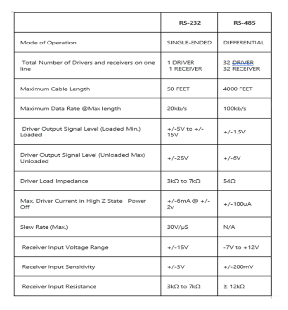
- The main drawbacks with RS-232 is lack of immunity for noise on the signal lines.
- The transmitter and receiver compare the voltages of data and handshake lines with one common zero line.
- The shifts in ground level produce disastrous effects. Therefore, the trigger level of RS-232 interface is set relatively high at ± 3V.
- In RS485 there is no common zero as signal reference. Several volts difference in ground level of RS485 transmitter and receiver does cause any problem.
- The RS485 signals are floating and each signal is transmitted over a Sig+ line and a Sig- line. The RS485 receiver compares the voltage difference between both lines,
- This works well and prevents the existence of ground loops, a common source of communication problems. The best results are achieved if the Sig+ and Sig- lines are twisted.
Key takeaway
- In RS485 there is no common zero as signal reference. Several volts difference in ground level of RS485 transmitter and receiver does cause any problem.
- The RS485 signals are floating and each signal is transmitted over a Sig+ line and a Sig- line. The RS485 receiver compares the voltage difference between both lines.
SPI
- Serial Peripheral Interface (SPI) is an interface bus used to send data between microcontrollers and small peripherals such as shift registers, sensors, and SD cards. It uses separate clock and data lines, along with a select line to choose the device to talk to.
- SPI has a "synchronous" data bus, which means that it uses separate lines for data and a "clock" that keeps both sides in perfect sync.
- The clock is an oscillating signal which tells the receiver exactly when to sample the bits on the data line. This could be the rising (low to high) or falling (high to low) edge of the clock signal. When the receiver detects that edge, it will immediately look at the data line to read the next bit. Because the clock is sent along with the data.

Figure 3. SPI
In SPI, only one side generates the clock signal called SCK for Serial ClocK. The side that generates the clock is called the "master", and the other side is called the "slave". There is always only one master, but there can be multiple slaves.
When data is sent from the master to a slave, it's sent on a data line called MOSI, for "Master Out / Slave In". If the slave needs to send a response back to the master, the master will continue to generate a prearranged number of clock cycles, and the slave will put the data onto a third data line called MISO, for "Master In / Slave Out".

Figure 4. Master-Slave

Figure 5. Multiple Slave
Key takeaway
- Serial Peripheral Interface (SPI) is an interface bus used to send data between microcontrollers and small peripherals such as shift registers, sensors, and SD cards. It uses separate clock and data lines, along with a select line to choose the device to talk to.
- SPI has a "synchronous" data bus, which means that it uses separate lines for data and a "clock" that keeps both sides in perfect sync.
Parallel Port single bit input
- Completion of a revolution of a wheel
- Achieving preset pressure in a boiler
- Exceeding the upper limit of permitted weight over the pan of an electronic balance
- Presence of a magnetic piece in the vicinity of or within reach of a robot arm to its end point and Filling of a liquid up to a fixed level.
Parallel Port Output- single bit
- PWM output for a DAC, which controls liquid level, or temperature, or pressure, or speed or angular position of a rotating shaft or a linear displacement of an object or a d.c. Motor control
- Pulses to an external circuit
- Control signal to an external circuit
Parallel Port Input- multi-bit
- ADC input from liquid level measuring sensor or temperature sensor or pressure sensor or speed sensor or d.c. Motor rpm sensor
- Encoder inputs for bits for angular position of a rotating shaft or a linear displacement of an object
Parallel Port Output- multi-bit
- LCD controller for Multilane LCD display matrix unit in a cellular phone to display on the screen the phone number, time, messages, character outputs or pictogram bit-images for display screen or e-mail or web page
- Print controller output
- Stepper-motor coil driving bits
Parallel Port Input-Output
- PPI 8255
- Touch screen in mobile phone
It is a serial protocol for two-wire interface to connect low-speed devices like microcontrollers, EEPROMS, A/D and D/A converters, I/O interfaces and so on.
- To send and receive commands all we need is two free I/O pins and few simple I2C routines. With I2C, data is transferred in messages.
- Messages are broken up into frames of data. Each message has an address frame that contains the binary address of the slave, and one or more data frames that contain the data being transmitted.
- The message also includes start and stop conditions, read/write bits, and ACK/NACK bits between each data frame:

Figure 6. Message bits
Start Condition: The SDA line switches from a high voltage level to a low voltage level before the SCL line switches from high to low.
Stop Condition: The SDA line switches from a low voltage level to a high voltage level after the SCL line switches from low to high.
Address Frame: A 7- or 10-bit sequence unique to each slave that identifies the slave when the master wants to talk to it.
Read/Write Bit: A single bit specifying whether the master is sending data to the slave (low voltage level) or requesting data from it (high voltage level).
ACK/NACK Bit: Each frame in a message is followed by an acknowledge/no-acknowledge bit. If an address frame or data frame was successfully received, an ACK bit is returned to the sender from the receiving device.
Steps of I2C Data Transmission
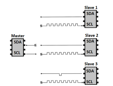
1. The master sends the start condition to every connected slave by switching the SDA line from a high voltage level to a low voltage level before switching the SCL line from high to low:

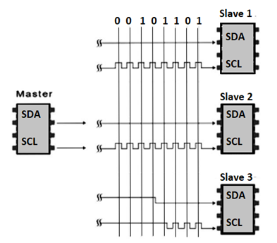
2. The master sends each slave the 7 or 10 bit address of the slave it wants to communicate with, along with the read/write bit:

3. Each slave compares the address sent from the master to its own address. If the address matches, the slave returns an ACK bit by pulling the SDA line low for one bit. If the address from the master does not match the slave’s own address, the slave leaves the SDA line high.
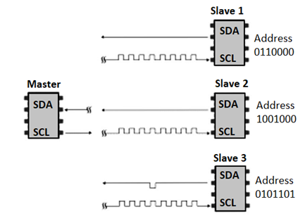
4. The master sends or receives the data frame:
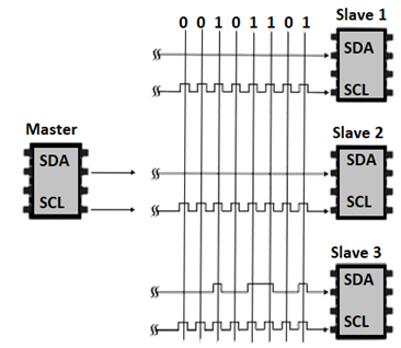
5. After each data frame has been transferred, the receiving device returns another ACK bit to the sender to acknowledge successful receipt of the frame:

6. To stop the data transmission, the master sends a stop condition to the slave by switching SCL high before switching SDA high:

Key takeaway
It is a serial protocol for two-wire interface to connect low-speed devices like microcontrollers, EEPROMS, A/D and D/A converters, I/O interfaces and so on.
- To send and receive commands all we need is two free I/O pins and few simple I2C routines. With I2C, data is transferred in messages.
- Messages are broken up into frames of data. Each message has an address frame that contains the binary address of the slave, and one or more data frames that contain the data being transmitted.
- The message also includes start and stop conditions, read/write bits, and ACK/NACK bits between each data frame.
It is also called the Universal Asynchronous Receiver Transmitter used in serial communication. It basically does serial to parallel data conversion on the transmitter side. Again, at the receiver side it converts the received data from serial to parallel. It is an interconnection between the processor and the serial communication port.

Above figure shows the connection of UART with the controller and USB interface. The timing settings between the transmitter and receiver in this case are of major concern. To maintain synchronisation UART uses special bits at the starting and end of each word.
The UART at the sender end receives the parallel data and converts it to serial data. The receiving side UARt receives this serial data and converts it to parallel and sends it back to the CPU.
Working of UART
The transmission in UART is asynchronous. The transmitter and receiver do not have any timing synchronisation. There are special bits which are used for synchronisation. They are called Start and Stop bits.
These bits are attached at the start and end of the data allowing the receiver to identify the actual data. The data bus transfers the data to the transmitting UART from the controlling device. This received data is in parallel.

The start, parity and stop bits are added to this received data. After inserting the special bits, they are converted to serial data with the help of shift registers. At the Rx pin the receiving UART receives this serial data. The original data is recognised by the special bits. Parity bit is used to check the integrity of the data.
The special bits are separated from the received data and it is again converted back to parallel data. Through the data bus this data is sent back to the receiving end of the controller.
Necessary requirement for UART
The requirements for data transmission are mentioned below.
- Synchronisation Bits (Start and Stop bits)
- Parity Bit
- Data Bits and
- Baud Rate
The rate of data transmission is called Baud rate. It is measured in bits per second.
Applications
UART is being used in many applications like GPS Receivers, Bluetooth Modules, GSM and GPRS Modems, Wireless Communication Systems, RFID based applications etc.
Advantages of UART
Requires only two wires for full duplex data transmission No need for clock or any other timing signal. Parity bit ensures basic error checking is integrated into the data packet frame.
Disadvantages of UART
Size of the data in the frame is limited. Speed for data transfer is less compared to parallel communication. Transmitter and receiver must agree to the rules of transmission and appropriate baud rate must be selected.
8251 universal synchronous asynchronous receiver transmitter (USART) acts as a mediator between microprocessor and peripheral to transmit serial data into parallel form and vice versa.
- It takes data serially from peripheral (outside devices) and converts into parallel data.
- After converting the data into parallel form, it transmits it to the CPU.
- Similarly, it receives parallel data from microprocessor and converts it into serial form.
- After converting data into serial form, it transmits it to outside device (peripheral).
Pin Configuration

Fig 7. Pin Configuration
Data Bus: Bi-directional, tri-state, 8-bit Data Bus. This pin allows transfer of bytes between the CPU and the 8251A.
RD (Read): A low on this input allows the CPU to read data or status bytes from 8251A
WR (Write): A low on this input allows the CPU to write data or command word to the 8251A.
CLK (Clock): The CLK input is used to generate internal device timing. The frequency of CLK must be greater than 30 times the receiver or transmitter data bit rates.
RESET: A high on this input forces the 8251A into an “Idle” mode. The device will remain at “Idle” until a new set of control words is written into the 8251 Pin Diagram to program its functional definition.
C/D (Control /Data): This input in conjuction with the WR and RD inputs, informs the 8251A that the word on the Data Bus is either a data character control word or status information as shown in table.
C/   | Operation |
0 0 1 | CPU reads data from USART |
0 1 0 | CPU writes Data to USART |
1 0 1 | CPU reads Status from USART |
1 1 1 | CPU writes command to USART |
X 1 1 | USART Bus Floating |
CS (Chip Select): A low on this input allows communication between CPU and 8251A

Fig 8. Block Diagram
It contains the following blocks:
- Data bus buffer –
This block helps in interfacing the internal data bus of 8251 to the system data bus. The data transmission is possible between 8251 and CPU by the data bus buffer block.
- Read/Write control logic –
It is a control block for overall device. It controls the overall working by selecting the operation to be done. The operation selection depends upon input signals as:
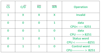
In this way, this unit selects one of the three registers- data buffer register, control register, status register.
- Modem control (modulator/demodulator) –
A device converts analog signals to digital signals and vice-versa and helps the computers to communicate over telephone lines or cable wires. The following are active-low pins of Modem.
- DSR: Data Set Ready signal is an input signal.
- DTR: Data terminal Ready is an output signal.
- CTS: It is an input signal which controls the data transmit circuit.
RTS: It is an output signal which is used to set the status RTS.
- Transmit buffer –
This block is used for parallel to serial converter that receives a parallel byte for conversion into serial signal and further transmission onto the common channel.
- TXD: It is an output signal, if its value is one, means transmitter will transmit the data.
- Transmit control –
This block is used to control the data transmission with the help of following pins:
- TXRDY: It means transmitter is ready to transmit data character.
- TXEMPTY: An output signal which indicates that TXEMPTY pin has transmitted all the data characters and transmitter is empty now.
- TXC: An active-low input pin which controls the data transmission rate of transmitted data.
- Receive buffer –
This block acts as a buffer for the received data.
- RXD: An input signal which receives the data.
- Receive control –
This block controls the receiving data.
- RXRDY: An input signal indicates that it is ready to receive the data.
- RXC: An active-low input signal which controls the data transmission rate of received data.
- SYNDET/BD: An input or output terminal. External synchronous mode-input terminal and asynchronous mode-output terminal.
Key takeaway
8251 universal synchronous asynchronous receiver transmitter (USART) acts as a mediator between microprocessor and peripheral to transmit serial data into parallel form and vice versa.
- It takes data serially from peripheral (outside devices) and converts into parallel data.
- After converting the data into parallel form, it transmits it to the CPU.
- Similarly, it receives parallel data from microprocessor and converts it into serial form.
- After converting data into serial form, it transmits it to outside device (peripheral).
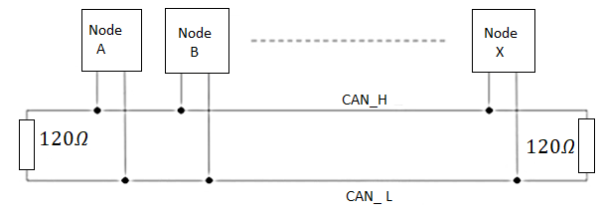
Controller Area Network (CAN) is a serial network technology that was originally designed for the automotive industry, especially for European cars, but has also become a popular bus in industrial automation as well as other applications. The CAN bus is primarily used in embedded systems, and as its name implies, is a network technology that provides fast communication among microcontrollers up to real-time requirements, eliminating the need for the much more expensive and complex technology of a Dual-Ported RAM.
CAN is a two-wire, half duplex, high-speed network system, that is far superior to conventional serial technologies such as RS232 in regards to functionality and reliability and yet CAN implementations are more cost effective.

While, for instance, TCP/IP is designed for the transport of large data amounts, CAN is designed for real-time requirements and with its 1 MBit/sec baud rate can easily beat a 100 MBit/sec TCP/IP connection when it comes to short reaction times, timely error detection, quick error recovery and error repair.
CAN networks can be used as an embedded communication system for microcontrollers as well as an open communication system for intelligent devices. Some users, for example in the field of medical engineering, opted for CAN because they have to meet particularly stringent safety requirements.
Similar requirements had to be considered by manufacturers of other equipment with very high safety or reliability requirements (e.g. Robots, lifts and transportation systems).
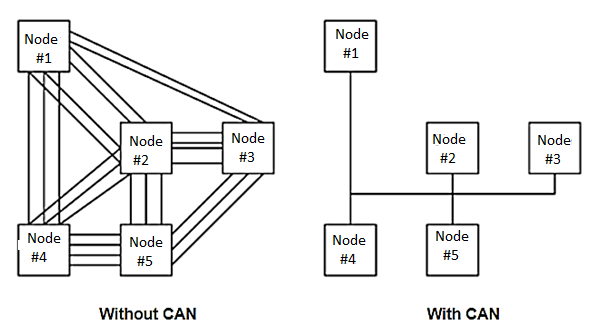
The greatest advantage of Controller Area Network lies in the reduced amount of wiring combined with an ingenious prevention of message collision (meaning no data will be lost during message transmission).

Key takeaway
- Is a serial networking technology for embedded solutions.
- Needs only two wires named CAN_H and CAN_L.
- Operates at data rates of up to 1 Megabit per second.
- Supports a maximum of 8 bytes per message frame.
- Does not support node IDs, only message IDs. One application can support multiple message IDs.
- Supports message priority, i.e. the lower the message ID the higher its priority.
- Supports two message ID lengths, 11-bit (standard) and 29-bit (extended).
- Does not experience message collisions (as they can occur under other serial technologies).
- Is not demanding in terms of cable requirements. Twisted-pair wiring is sufficient.
Bluetooth
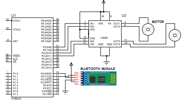
Bluetooth is appropriate. Teri Open wireless protocol for exchanging data over short distances from fixed and mobile devices, creating personal area networks. It was originally convinced as a wireless alternative to RS-232 data cables. Bluetooth is a promising standard for short range wireless communication. Bluetooth uses the same frequency as Wave Lan but with much less effect. But anyhow, some claim that Wave Lan cannot coexist with a fully equipped Bluetooth environment. Bluetooth is a wireless technology for transmission of voice and data over a short distance. R XD and TXD pins on Bluetooth evaluation kit connected with. Controller through serial port.
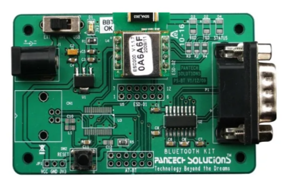
Fig 9. Bluetooth interface board

USB protocols
Universal serial bus is a set of interface specifications for high speed wired communication between electronics systems peripherals and devices with or without PC/ computer. The USB was originally developed in 1995 by many of the industry leading companies like Intel, Compaq, Microsoft, Digital, IBM and Northern Telecom. The major goal of USB was to define an external expansion bus to add peripherals to a PC in easy and simple manner.
USB offers users simple connectivity. It eliminates the mix of different connectors for different devices like printers, keyboards, mice and other peripherals. That means USB-bus allows many peripherals to be connected using a single standardized interface socket. It supports all kinds of data, from slow mouse inputs to digitized audio and compressed video.
USB also allows hot swapping. The hot-swapping means that devices can be plugged and unplugged without rebooting the computer or turning off the devices. That means, when unplugged in, everything configures automatically. Once the user finished, they can simply unplug the cable out, the host will detect its absence and automatically unload the driver. This makes the USB a plug-and-play interface between a computer and add-on devices.
USB is now the most used interface to connect devices like mouse, keyboards, PDAs, game-pads and joysticks, scanners, scanners, digital cameras, printers, personal media players and flash drives to personal computers. USB sends data in serial mode i.e. the parallel data is serialized before sends and deserialized after receiving.
The benefits of USB are low cost, expandability, auto-configuration, hot- plugging and outstanding performance. It also provides power to the bus, enabling many peripherals to operate without the added need for AC power adapter.
Various version USB
USB1.0: USB 1.0 is the original release of USB having the capability of transferring 12 Mbps, supporting up to 127 devices. The USB 1.0 specification model was introduced in January 1996.
USB1.1: USB 1.1 came out in September 1998. USB 1.1 is known as full speed USB. The version is similar to the original release of USB; however, there are minor modifications for the hardware and the specifications. USB version 1.1 supported two speeds, a full speed mode of 12Mbits/s and a low-speed mode of 1.5 M bits/s.
USB2.0: HP, Intel, LSI corporation, Microsoft, NE, and Philips jointly led the initiative to develop a higher data transfer rate than the 1.1 specifications. The USB 2.0 specifications was released in April 2000 and was standardized at the end of 2001.
Supporting three speed motors (1.5, 12 and 480Mbps), USB 2.0 supports low-bandwidth devices such as keyboards and mice, as well as high-bandwidth ones like high-resolution web-cams, scanners, printers and high-capacity storage systems.
USB 2.0 also known as hi-speed USB. This hi-speed USB is capable of supporting a transfer rate of up to 480 Mbps, compared to 12Mbps of USB 1.1.
USB3.0: USB 3.0 is the latest version of USB release. It is also called as super speed USB having a data transfer rate of 4.8 Gbps (600MB/s). That means it can deliver over 10x the speed of today’s Hi-speed USB connections. The USB 3.0 specifications was released by Intel and its partners in August 2008. Product using the 3.0 specifications are come out in 2010.
The USB tiered star topology
The USB system is made up of a host, multiple numbers of USB ports, and multiple peripheral devices connected in a tiered star topology. The host is the USB systems master and as such controls and schedules all communications activities. Peripherals the devices controlled by USBR slaves responding to commands from the host USB devices are linked in series through hubs. There always exist one hub known as the root hub, which is built into the host controller.

USB connectors: connecting a USB device to a computer is very simple. You find the USB connector on the back of your machine and plug to USB connector into it. If it is a new device, the operating system auto detect set and asks for the driver desk. If the device has already been installed, the computer activates it and starts talking to it. The USB standard specifies two kinds of cables and connectors, as shown below. The USB standard uses A and B connectors mainly to avoid confusion: A connectors head upstream towards the computer, B connectors, head down streams and connect to individual devices. By using different connectors on the upstream and downstream end, it is impossible to install a cable incorrectly, because the two types are physically different.

USB can support for data transfer types or transfer mobiles. Control isochronous bulk interrupt. Next paragraph. Control transfers, exchange configuration setup, and command information between the device and host. The host can also send commands or query parameters, with control packets. Isochronous transfer is used. My time Critical commerce streaming device. Such a speakers, video cameras. It s time sensitive information. So, within limitations, it has guaranteed access to the USB. Bulk transfer is used by devices like printers and scanners, which receives data in one big packet. Interrupt transfer, is used by peripherals exchanging small amount of data that need immediate attention. All USB data send serial. USB data transfer is essential in the form of packets of data commerce send back and forth between the host and peripheral devices. Initially, all packets are sent from the host, via the root hub and possibly more hubs, to devices. Each USB data transfer consists of
1. Token packet
2. Optional Data Packet
3. Statis Packet
Timer
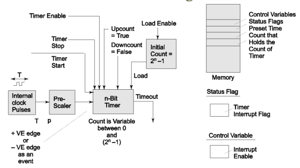
- A device, which counts the input at regular interval (T) using clock pulses at its input.
- The counts increment on each pulse
- Store in a register, called count register
- Output bits (in a count register or at the output pins) for the present counts.
Evaluation of Time
- The counts multiplied by the interval T give the time.
- The (present counts initial counts) T interval gives the time interval between two instances when present count bits are read and initial counts were read or set.
Timer
- Has an input pin (or a control bit in control register) for resetting it for all count bits = 0s.
- Has an output pin (or a status bit in status register) for output when all count bits = 0s after reaching the maximum value, which also means after timeout or overflow.
Counter
- A device, which counts the input due to the events at irregular or regular intervals.
- The count gives the number of input events or pulses since it was last read.
- Has a register to enable read of present counts
- Functions as timer when counting regular interval clock pulses
- Has an input pin (or a control bit in control register) for resetting it for all count bits = 0s.
- Has an output pin (or a status bit in status register) for output when all count bits = 0s after reaching the maximum value, which also means after timeout or overflow.
Timer or Counter Interrupt
When a timer or counter becomes 0x00 or 0x0000 after 0xFF or 0xFFFF (maximum value), it can generate an ‘interrupt’, or an output ‘Time-Out’ or set a status bit ‘TOV’.

Free running Counter (Blind running Counter)
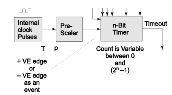
- A counting device may be a free running (blind counting) device giving overflow interrupts at fixed intervals.
- A pre-scalar for the clock input pulses to fix the intervals.
Free Running Counter
It is useful
- For action or initiating chain of actions
- Processor interrupts at the preset instances
- Noting the instances of occurrences of the events
- Processor interrupts for requesting the processor to use the capturing of counts at the input instance
- Comparing of counts on the events for future actions

Free running (blind counting) device Many Applications Based on
- Comparing the count (instance) with the one preloaded in a compare register [an additional register for defining an instance for an action]
- Capturing counts (instance) in an additional register on an input event. [An addition input pin for sensing an event and saving the counts at the instance of event and taking action.]
Free running (Blind Counts) input OC enable pin (or a control bit in control register)
- For enabling an output when all count bits at free running count = preloaded counts in the compare register.
- At that instance a status bit or output pin also sets in and an interrupt ‘OCINT’ of processor can occur for event of comparison equality.
- Generates alarm or processor interrupts at the preset times or after preset interval from another event
Free running (Blind Counts) input capture -enable pin (or a control bit in control register) for Instance of Event Capture
- A register for capturing the counts on an instance of an input (0 to 1 or 1 to 0 or toggling) transition
- A status bit can also set in and processor interrupt can occur for the capture event
Free running (Blind Counts) Pre-scaling
- Prescalar can be programmed as p = 1, 2, 4, 8, 16, 32, .. By programming a prescaler register. Prescalar divides the input pulses as per the programmed value of p.
- Count interval = p T interval
- T = clock pulses period, clock frequency = T1
Free running (Blind Counts) Overflow
- It has an output pin (or a status bit in status register) for output when all count bits = 0s after reaching the maximum value, which also means after timeout or overflow
- Free running n-bit counter overflows after p 2n T interval
Uses of Timer/Counter Related Devices
- Real Time Clock Ticks (System Heart Beats). [Real time clock is a clock, which, once the system starts, does not stop and can't be reset and its count value can't be reloaded. Real time endlessly flows and never returns back!] Real Time Clock is set for ticks using prescaling bits (or rate set bits) in appropriate control registers.
- Initiating an event after a preset delay time. Delay is as per count value loaded.
Use of Timer Devices
- Initiating an event (or a pair of events or a chain of events) after a comparison(s) with between the pre-set time(s) with counted value(s). [It is similar to a preset alarm(s).]
- A preset time is loaded in a Compare Register. [It is similar to presetting an alarm].
- Capturing the count value at the timer on an event. The information of time (instance of the event) is thus stored at the capture register.
- Finding the time interval between two events. Counts are captured at each event in capture register(s) and read. The intervals are thus found out.
- Wait for a message from a queue or mailbox or semaphore for a preset time when using RTOS. There is a A predefined waiting period is done before RTOS lets a task run.
- Watchdog timer. It resets the system after a defined time.
- Baud or Bit Rate Control for serial communication on a line or network. Timer timeout interrupts define the time of each baud
- Input pulse counting when using a timer, which is ticked by giving nonperiodic inputs instead of the clock inputs. The timer acts as a counter if, in place of clock inputs, the inputs are given to the timer for each instance to be counted.
- Scheduling of various tasks
- A chain of software-timers interrupt and RTOS uses these interrupts to schedule the tasks.
- Time slicing of various tasks. A multitasking or multi-programmed operating system presents the illusion that multiple tasks or programs are running simultaneously by switching between programs very rapidly, for example, after every 16.6 ms.
- Process known as a context switch. [RTOS switches after preset time-delay from one running task to the next. Task. Each task can therefore run in predefined slots of time]
- Time division multiplexing (TDM)
- Timer device used for multiplexing the input from a number of channels.
- Each channel input allotted a distinct and fixed-time slot to get a TDM output. [For example, multiple telephone calls are the inputs and TDM device generates the TDM output for launching it into the optical fiber.
Timer States
- Reset State (initial count = 0)
- Initial Load State (initial count loaded)
- Present State (counting or idle or before start or after overflow or overrun)
- Overflow State (count received to make count = 0 after reaching the maximum count)
- Overrun State (several counts received after reaching the overflow state)
- Running (Active) or Stop (Blocked) state
- Finished (Done) state (stopped after a preset time interval or timeout)
- Reset enabled/disabled State (enabled resetting of count = 0 by an input)
- Load enabled/disabled State (reset count = initial count after the timeout)
- Auto Re-Load enabled/disabled State (enabled count = initial count after the timeout)
- Service Routine Execution enable/disable State (enabled after timeout or overflow)
Software timer
- A timer which executes a software after the counts increment by certain pre-defined value and interrupt from to a system and executes a set of software instructions (ISR)
- The software timer which generates interrupt on overflow of count-value or on finishing value of the count variable and runs a set of instructions (ISR).
System clock
- A hardware-timing device programmed to tick at constant intervals T.
- An interrupt at each tick
- A chain of interrupts thus occurs at periodic intervals.
- T is as per a preset count value
- The interrupts are called system clock interrupts, when used to control the schedules and timings in the system
- System clock has fixed program to tick at constant intervals T.
- SWTs have fixed but programmable to tick at intervals T.
- An interrupt at each tick in both
- The interrupts called system clock and SWT interrupts, respectively
Watchdog timer is a hardware microcontroller. It is basically used to take out a system from an infinite loop and resets the system. Watchdog makes the embedded systems more reliable as it works as a safety mechanism.
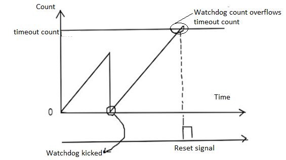
Watchdog is a type of counter. It is an up counter which means that it counts from zero and reaches to some values. As soon the watchdog timer reaches some value its hardware generates a watchdog reset. Then the system resets this count value to zero in order to avoid system reset. The watchdog timer is loaded with some values which are based on its timeout time. The system needs to reset the counter before timeout.
Watchdog Timer Hardware
The figure below is of watchdog time hardware with input as clock. With every clock the internal counter increments. Then the comparator will compare this value with the loaded count value. Then if the comparator finds that count value matches the watchdog hardware generates and resets it.
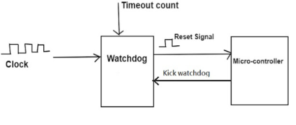

Watchdog in Microcontroller MSPXXX Family
The internal watchdog of the MSP430 family is used either as a simple timer or as a watchdog that ensures system integrity. The watchdog function is enabled after power-on reset or system reset. In case of any difficulties after start-up of MSP430, the watchdog will reset the system as often as it is needed for it to start successfully.
A system running with MCLK = 3 MHz uses the watchdog for supervision of three functions.
Power Fail — by checking the 60 Hz AC line.
Function 1 — A check is made if the software reaches this background part regularly
Function 3 — A check is made if this interrupt handler is called regularly.
Each supervised function sets a dedicated bit in RAM byte WDB in intervals less than 10.66 ms (power-up value of the watchdog with MCLK = 3 MHz) if everything is functioning normally.
The main loop checks this byte (WDB) and resets the watchdog ONLY if all three bits are set (07h). If one of the functions fails, the watchdog is not reset and will therefore reset the system.
Real time clock
Features:
- Real-time clock (RTC) counts seconds, minutes, hours, date of the month, month, day of the week, and year with leap-year compensation valid up to 2100
- 56-byte, battery-backed, non-volatile (NV) RAM for data storage
- Two-wire serial interface
- Programmable square wave output signal
- Automatic power-fail detect and switch circuitry
- Consumes less than 500nA in battery backup mode with oscillator running
- Optional industrial temperature range: -40°C to +85°C

Fig 10. DS 1307 Pin Diagram
Device Addressing
DS 1307 requires 8-bit device word follwing the start condition.
To enable the chip to read or write operation.

The device address word consists of a mandatory zero seequence for MSB as shown.
RTC and RAM address map
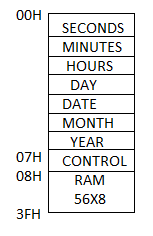
The address map for the RTC and RAM registers of the DS1307 are shown, The RTC registers are in address locations
Ooh to 07h. The RAM registers are in address locations 08h to 3Fh. During a multi-byte access, when the address pointer reaches 3Fh, the end of RAM space, it wraps around to location Ooh, the beginning of the clock space.
RTC clock
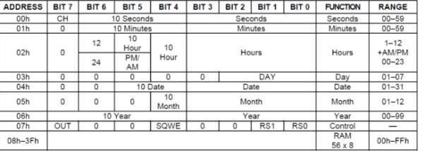
Write Operation:

- Serial data and clock are received through SDA and SCL.
- After each byte is received an acknowledge bit is transmitted.
- START and STOP conditions are recognized as the beginning and end of a serial transfer. Hardware performs address recognition after reception of the slave address and direction bit (see Figure).
- The slave address byte is the first byte received after the master generates the START condition.
- The slave address byte contains the 7-bit DS1307 address, which is 1101000, followed by the direction bit (R/W), which for a write is 0.
- After receiving and decoding the slave address byte, the DS1307 outputs an acknowledge on SDA. After the DS1307 acknowledges the slave address + write bit, the master transmits a word address to the DS1307.
- This sets the register pointer on the DS1307, with the DS1307 acknowledging the transfer.
- The master can then transmit zero or more bytes of data with the DS1307 acknowledging each byte received.
- The register pointer automatically increments after each data byte are written.
- The master will generate a STOP condition to terminate the data write.
Read Operation:

Fig 11. Write memory pointer
- The first byte is received and handled as in the slave receiver mode. However, in this mode, the direction bit will indicate that the transfer direction is reversed.
- The DS1307 transmits serial data on SDA while the serial clock is input on SCL.
- START and STOP conditions are recognized as the beginning and end of a serial transfer (see Figure).
- The slave address byte is the first byte received after the START condition is generated by the master. The slave address byte contains the 7-bit DS1307 address, which is 1101000, followed by the direction bit (R/W), which is 1 for a read.
- After receiving and decoding the slave address the DS1307 outputs an acknowledge on SDA.
- The DS1307 then begins to transmit data starting with the register address pointed to by the register pointer. If the register pointer is not written to before the initiation of a read mode the first address that is read is the last one stored in the register pointer.
- The register pointer automatically increments after each byte are read.
- The DS1307 must receive a Not Acknowledge to end a read.

Figure 12. Interfacing
Key takeaway
- After each byte is received an acknowledge bit is transmitted.
- START and STOP conditions are recognized as the beginning and end of a serial transfer. Hardware performs address recognition after reception of the slave address and direction bit (see Figure).
- The slave address byte is the first byte received after the master generates the START condition.
- The slave address byte contains the 7-bit DS1307 address, which is 1101000, followed by the direction bit (R/W), which for a write is 0.
References:
1. M. A. Mazidi, J. G. Mazidi and R. D. McKinlay, “The8051Microcontroller and Embedded Systems:
Using Assembly and C”, Pearson Education, 2007.
2. K. J. Ayala, “8051 Microcontroller”, Delmar Cengage Learning,2004.
3. The 8051 Microcontroller Based Embedded System By Manish K. Patel TMH.
4. Embedded System Architecture, Programming and Design by Raj Kamal, 3rd Edition TMH.
5. Introduction to Embedded System by Shibu K. V. 3rd Edition TMH
Unit - 5
Devices and Communication
RS-232 represents serial data transmission. RS232 transmits signals using a positive voltage for binary 0 and negative voltage for binary 1.
To talk to other modules PLCs, use RS232. These modules may be anything that use RS232 as operator, interface or HMI, computers, motor controller’s robot or vision system.
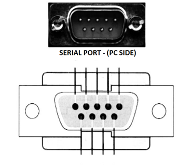
Figure 1. DB-9 connector

RS-232 Line Driver
- It consists of two-line drivers, two-line receivers, and a dual charge-pump circuit with ±15 kV ESD protection.
- It provides the electrical interface between an asynchronous communication controller and a serial port connector.

Figure 2. RS-232 Line Driver
- The maximum speed is 20kbit/s. However, modern equipment can operate much faster than this.
- The length of the cable also plays a part in maximum speed. The longer the cable and slower the speed you can obtain accurate results.
Key takeaway
RS-232 represents serial data transmission. RS232 transmits signals using a positive voltage for binary 0 and negative voltage for binary 1
RS-485
- The main drawbacks with RS-232 is lack of immunity for noise on the signal lines.
- The transmitter and receiver compare the voltages of data and handshake lines with one common zero line.
- The shifts in ground level produce disastrous effects. Therefore, the trigger level of RS-232 interface is set relatively high at ± 3V.
- In RS485 there is no common zero as signal reference. Several volts difference in ground level of RS485 transmitter and receiver does cause any problem.
- The RS485 signals are floating and each signal is transmitted over a Sig+ line and a Sig- line. The RS485 receiver compares the voltage difference between both lines,
- This works well and prevents the existence of ground loops, a common source of communication problems. The best results are achieved if the Sig+ and Sig- lines are twisted.

Key takeaway
- In RS485 there is no common zero as signal reference. Several volts difference in ground level of RS485 transmitter and receiver does cause any problem.
- The RS485 signals are floating and each signal is transmitted over a Sig+ line and a Sig- line. The RS485 receiver compares the voltage difference between both lines.
SPI
- Serial Peripheral Interface (SPI) is an interface bus used to send data between microcontrollers and small peripherals such as shift registers, sensors, and SD cards. It uses separate clock and data lines, along with a select line to choose the device to talk to.
- SPI has a "synchronous" data bus, which means that it uses separate lines for data and a "clock" that keeps both sides in perfect sync.
- The clock is an oscillating signal which tells the receiver exactly when to sample the bits on the data line. This could be the rising (low to high) or falling (high to low) edge of the clock signal. When the receiver detects that edge, it will immediately look at the data line to read the next bit. Because the clock is sent along with the data.
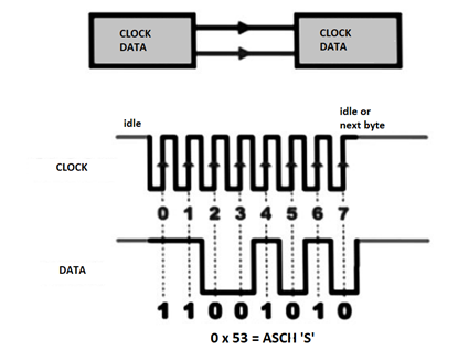
Figure 3. SPI
In SPI, only one side generates the clock signal called SCK for Serial ClocK. The side that generates the clock is called the "master", and the other side is called the "slave". There is always only one master, but there can be multiple slaves.
When data is sent from the master to a slave, it's sent on a data line called MOSI, for "Master Out / Slave In". If the slave needs to send a response back to the master, the master will continue to generate a prearranged number of clock cycles, and the slave will put the data onto a third data line called MISO, for "Master In / Slave Out".
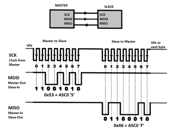
Figure 4. Master-Slave
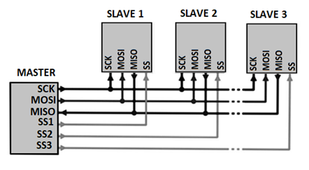
Figure 5. Multiple Slave
Key takeaway
- Serial Peripheral Interface (SPI) is an interface bus used to send data between microcontrollers and small peripherals such as shift registers, sensors, and SD cards. It uses separate clock and data lines, along with a select line to choose the device to talk to.
- SPI has a "synchronous" data bus, which means that it uses separate lines for data and a "clock" that keeps both sides in perfect sync.
Parallel Port single bit input
- Completion of a revolution of a wheel
- Achieving preset pressure in a boiler
- Exceeding the upper limit of permitted weight over the pan of an electronic balance
- Presence of a magnetic piece in the vicinity of or within reach of a robot arm to its end point and Filling of a liquid up to a fixed level.
Parallel Port Output- single bit
- PWM output for a DAC, which controls liquid level, or temperature, or pressure, or speed or angular position of a rotating shaft or a linear displacement of an object or a d.c. Motor control
- Pulses to an external circuit
- Control signal to an external circuit
Parallel Port Input- multi-bit
- ADC input from liquid level measuring sensor or temperature sensor or pressure sensor or speed sensor or d.c. Motor rpm sensor
- Encoder inputs for bits for angular position of a rotating shaft or a linear displacement of an object
Parallel Port Output- multi-bit
- LCD controller for Multilane LCD display matrix unit in a cellular phone to display on the screen the phone number, time, messages, character outputs or pictogram bit-images for display screen or e-mail or web page
- Print controller output
- Stepper-motor coil driving bits
Parallel Port Input-Output
- PPI 8255
- Touch screen in mobile phone
It is a serial protocol for two-wire interface to connect low-speed devices like microcontrollers, EEPROMS, A/D and D/A converters, I/O interfaces and so on.
- To send and receive commands all we need is two free I/O pins and few simple I2C routines. With I2C, data is transferred in messages.
- Messages are broken up into frames of data. Each message has an address frame that contains the binary address of the slave, and one or more data frames that contain the data being transmitted.
- The message also includes start and stop conditions, read/write bits, and ACK/NACK bits between each data frame:

Figure 6. Message bits
Start Condition: The SDA line switches from a high voltage level to a low voltage level before the SCL line switches from high to low.
Stop Condition: The SDA line switches from a low voltage level to a high voltage level after the SCL line switches from low to high.
Address Frame: A 7- or 10-bit sequence unique to each slave that identifies the slave when the master wants to talk to it.
Read/Write Bit: A single bit specifying whether the master is sending data to the slave (low voltage level) or requesting data from it (high voltage level).
ACK/NACK Bit: Each frame in a message is followed by an acknowledge/no-acknowledge bit. If an address frame or data frame was successfully received, an ACK bit is returned to the sender from the receiving device.
Steps of I2C Data Transmission
1. The master sends the start condition to every connected slave by switching the SDA line from a high voltage level to a low voltage level before switching the SCL line from high to low:
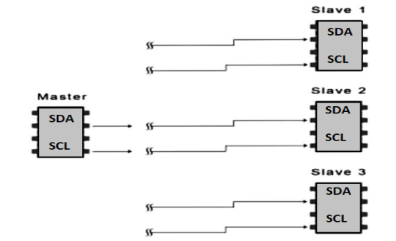
2. The master sends each slave the 7 or 10 bit address of the slave it wants to communicate with, along with the read/write bit:
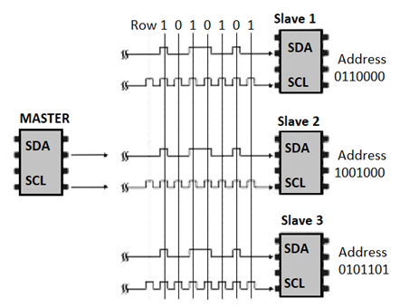
3. Each slave compares the address sent from the master to its own address. If the address matches, the slave returns an ACK bit by pulling the SDA line low for one bit. If the address from the master does not match the slave’s own address, the slave leaves the SDA line high.

4. The master sends or receives the data frame:

5. After each data frame has been transferred, the receiving device returns another ACK bit to the sender to acknowledge successful receipt of the frame:
6. To stop the data transmission, the master sends a stop condition to the slave by switching SCL high before switching SDA high:
Key takeaway
It is a serial protocol for two-wire interface to connect low-speed devices like microcontrollers, EEPROMS, A/D and D/A converters, I/O interfaces and so on.
- To send and receive commands all we need is two free I/O pins and few simple I2C routines. With I2C, data is transferred in messages.
- Messages are broken up into frames of data. Each message has an address frame that contains the binary address of the slave, and one or more data frames that contain the data being transmitted.
- The message also includes start and stop conditions, read/write bits, and ACK/NACK bits between each data frame.
It is also called the Universal Asynchronous Receiver Transmitter used in serial communication. It basically does serial to parallel data conversion on the transmitter side. Again, at the receiver side it converts the received data from serial to parallel. It is an interconnection between the processor and the serial communication port.

Above figure shows the connection of UART with the controller and USB interface. The timing settings between the transmitter and receiver in this case are of major concern. To maintain synchronisation UART uses special bits at the starting and end of each word.
The UART at the sender end receives the parallel data and converts it to serial data. The receiving side UARt receives this serial data and converts it to parallel and sends it back to the CPU.
Working of UART
The transmission in UART is asynchronous. The transmitter and receiver do not have any timing synchronisation. There are special bits which are used for synchronisation. They are called Start and Stop bits.
These bits are attached at the start and end of the data allowing the receiver to identify the actual data. The data bus transfers the data to the transmitting UART from the controlling device. This received data is in parallel.
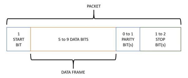
The start, parity and stop bits are added to this received data. After inserting the special bits, they are converted to serial data with the help of shift registers. At the Rx pin the receiving UART receives this serial data. The original data is recognised by the special bits. Parity bit is used to check the integrity of the data.
The special bits are separated from the received data and it is again converted back to parallel data. Through the data bus this data is sent back to the receiving end of the controller.
Necessary requirement for UART
The requirements for data transmission are mentioned below.
- Synchronisation Bits (Start and Stop bits)
- Parity Bit
- Data Bits and
- Baud Rate
The rate of data transmission is called Baud rate. It is measured in bits per second.
Applications
UART is being used in many applications like GPS Receivers, Bluetooth Modules, GSM and GPRS Modems, Wireless Communication Systems, RFID based applications etc.
Advantages of UART
Requires only two wires for full duplex data transmission No need for clock or any other timing signal. Parity bit ensures basic error checking is integrated into the data packet frame.
Disadvantages of UART
Size of the data in the frame is limited. Speed for data transfer is less compared to parallel communication. Transmitter and receiver must agree to the rules of transmission and appropriate baud rate must be selected.
8251 universal synchronous asynchronous receiver transmitter (USART) acts as a mediator between microprocessor and peripheral to transmit serial data into parallel form and vice versa.
- It takes data serially from peripheral (outside devices) and converts into parallel data.
- After converting the data into parallel form, it transmits it to the CPU.
- Similarly, it receives parallel data from microprocessor and converts it into serial form.
- After converting data into serial form, it transmits it to outside device (peripheral).
Pin Configuration
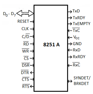
Fig 7. Pin Configuration
Data Bus: Bi-directional, tri-state, 8-bit Data Bus. This pin allows transfer of bytes between the CPU and the 8251A.
RD (Read): A low on this input allows the CPU to read data or status bytes from 8251A
WR (Write): A low on this input allows the CPU to write data or command word to the 8251A.
CLK (Clock): The CLK input is used to generate internal device timing. The frequency of CLK must be greater than 30 times the receiver or transmitter data bit rates.
RESET: A high on this input forces the 8251A into an “Idle” mode. The device will remain at “Idle” until a new set of control words is written into the 8251 Pin Diagram to program its functional definition.
C/D (Control /Data): This input in conjuction with the WR and RD inputs, informs the 8251A that the word on the Data Bus is either a data character control word or status information as shown in table.
C/   | Operation |
0 0 1 | CPU reads data from USART |
0 1 0 | CPU writes Data to USART |
1 0 1 | CPU reads Status from USART |
1 1 1 | CPU writes command to USART |
X 1 1 | USART Bus Floating |
CS (Chip Select): A low on this input allows communication between CPU and 8251A
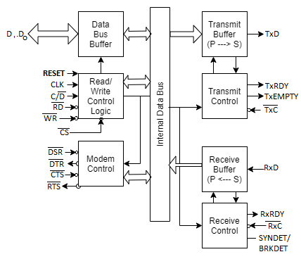
Fig 8. Block Diagram
It contains the following blocks:
- Data bus buffer –
This block helps in interfacing the internal data bus of 8251 to the system data bus. The data transmission is possible between 8251 and CPU by the data bus buffer block.
- Read/Write control logic –
It is a control block for overall device. It controls the overall working by selecting the operation to be done. The operation selection depends upon input signals as:

In this way, this unit selects one of the three registers- data buffer register, control register, status register.
- Modem control (modulator/demodulator) –
A device converts analog signals to digital signals and vice-versa and helps the computers to communicate over telephone lines or cable wires. The following are active-low pins of Modem.
- DSR: Data Set Ready signal is an input signal.
- DTR: Data terminal Ready is an output signal.
- CTS: It is an input signal which controls the data transmit circuit.
RTS: It is an output signal which is used to set the status RTS.
- Transmit buffer –
This block is used for parallel to serial converter that receives a parallel byte for conversion into serial signal and further transmission onto the common channel.
- TXD: It is an output signal, if its value is one, means transmitter will transmit the data.
- Transmit control –
This block is used to control the data transmission with the help of following pins:
- TXRDY: It means transmitter is ready to transmit data character.
- TXEMPTY: An output signal which indicates that TXEMPTY pin has transmitted all the data characters and transmitter is empty now.
- TXC: An active-low input pin which controls the data transmission rate of transmitted data.
- Receive buffer –
This block acts as a buffer for the received data.
- RXD: An input signal which receives the data.
- Receive control –
This block controls the receiving data.
- RXRDY: An input signal indicates that it is ready to receive the data.
- RXC: An active-low input signal which controls the data transmission rate of received data.
- SYNDET/BD: An input or output terminal. External synchronous mode-input terminal and asynchronous mode-output terminal.
Key takeaway
8251 universal synchronous asynchronous receiver transmitter (USART) acts as a mediator between microprocessor and peripheral to transmit serial data into parallel form and vice versa.
- It takes data serially from peripheral (outside devices) and converts into parallel data.
- After converting the data into parallel form, it transmits it to the CPU.
- Similarly, it receives parallel data from microprocessor and converts it into serial form.
- After converting data into serial form, it transmits it to outside device (peripheral).
Controller Area Network (CAN) is a serial network technology that was originally designed for the automotive industry, especially for European cars, but has also become a popular bus in industrial automation as well as other applications. The CAN bus is primarily used in embedded systems, and as its name implies, is a network technology that provides fast communication among microcontrollers up to real-time requirements, eliminating the need for the much more expensive and complex technology of a Dual-Ported RAM.
CAN is a two-wire, half duplex, high-speed network system, that is far superior to conventional serial technologies such as RS232 in regards to functionality and reliability and yet CAN implementations are more cost effective.
While, for instance, TCP/IP is designed for the transport of large data amounts, CAN is designed for real-time requirements and with its 1 MBit/sec baud rate can easily beat a 100 MBit/sec TCP/IP connection when it comes to short reaction times, timely error detection, quick error recovery and error repair.
CAN networks can be used as an embedded communication system for microcontrollers as well as an open communication system for intelligent devices. Some users, for example in the field of medical engineering, opted for CAN because they have to meet particularly stringent safety requirements.
Similar requirements had to be considered by manufacturers of other equipment with very high safety or reliability requirements (e.g. Robots, lifts and transportation systems).
The greatest advantage of Controller Area Network lies in the reduced amount of wiring combined with an ingenious prevention of message collision (meaning no data will be lost during message transmission).
Key takeaway
- Is a serial networking technology for embedded solutions.
- Needs only two wires named CAN_H and CAN_L.
- Operates at data rates of up to 1 Megabit per second.
- Supports a maximum of 8 bytes per message frame.
- Does not support node IDs, only message IDs. One application can support multiple message IDs.
- Supports message priority, i.e. the lower the message ID the higher its priority.
- Supports two message ID lengths, 11-bit (standard) and 29-bit (extended).
- Does not experience message collisions (as they can occur under other serial technologies).
- Is not demanding in terms of cable requirements. Twisted-pair wiring is sufficient.
Bluetooth
Bluetooth is appropriate. Teri Open wireless protocol for exchanging data over short distances from fixed and mobile devices, creating personal area networks. It was originally convinced as a wireless alternative to RS-232 data cables. Bluetooth is a promising standard for short range wireless communication. Bluetooth uses the same frequency as Wave Lan but with much less effect. But anyhow, some claim that Wave Lan cannot coexist with a fully equipped Bluetooth environment. Bluetooth is a wireless technology for transmission of voice and data over a short distance. R XD and TXD pins on Bluetooth evaluation kit connected with. Controller through serial port.

Fig 9. Bluetooth interface board
USB protocols
Universal serial bus is a set of interface specifications for high speed wired communication between electronics systems peripherals and devices with or without PC/ computer. The USB was originally developed in 1995 by many of the industry leading companies like Intel, Compaq, Microsoft, Digital, IBM and Northern Telecom. The major goal of USB was to define an external expansion bus to add peripherals to a PC in easy and simple manner.
USB offers users simple connectivity. It eliminates the mix of different connectors for different devices like printers, keyboards, mice and other peripherals. That means USB-bus allows many peripherals to be connected using a single standardized interface socket. It supports all kinds of data, from slow mouse inputs to digitized audio and compressed video.
USB also allows hot swapping. The hot-swapping means that devices can be plugged and unplugged without rebooting the computer or turning off the devices. That means, when unplugged in, everything configures automatically. Once the user finished, they can simply unplug the cable out, the host will detect its absence and automatically unload the driver. This makes the USB a plug-and-play interface between a computer and add-on devices.
USB is now the most used interface to connect devices like mouse, keyboards, PDAs, game-pads and joysticks, scanners, scanners, digital cameras, printers, personal media players and flash drives to personal computers. USB sends data in serial mode i.e. the parallel data is serialized before sends and deserialized after receiving.
The benefits of USB are low cost, expandability, auto-configuration, hot- plugging and outstanding performance. It also provides power to the bus, enabling many peripherals to operate without the added need for AC power adapter.
Various version USB
USB1.0: USB 1.0 is the original release of USB having the capability of transferring 12 Mbps, supporting up to 127 devices. The USB 1.0 specification model was introduced in January 1996.
USB1.1: USB 1.1 came out in September 1998. USB 1.1 is known as full speed USB. The version is similar to the original release of USB; however, there are minor modifications for the hardware and the specifications. USB version 1.1 supported two speeds, a full speed mode of 12Mbits/s and a low-speed mode of 1.5 M bits/s.
USB2.0: HP, Intel, LSI corporation, Microsoft, NE, and Philips jointly led the initiative to develop a higher data transfer rate than the 1.1 specifications. The USB 2.0 specifications was released in April 2000 and was standardized at the end of 2001.
Supporting three speed motors (1.5, 12 and 480Mbps), USB 2.0 supports low-bandwidth devices such as keyboards and mice, as well as high-bandwidth ones like high-resolution web-cams, scanners, printers and high-capacity storage systems.
USB 2.0 also known as hi-speed USB. This hi-speed USB is capable of supporting a transfer rate of up to 480 Mbps, compared to 12Mbps of USB 1.1.
USB3.0: USB 3.0 is the latest version of USB release. It is also called as super speed USB having a data transfer rate of 4.8 Gbps (600MB/s). That means it can deliver over 10x the speed of today’s Hi-speed USB connections. The USB 3.0 specifications was released by Intel and its partners in August 2008. Product using the 3.0 specifications are come out in 2010.
The USB tiered star topology
The USB system is made up of a host, multiple numbers of USB ports, and multiple peripheral devices connected in a tiered star topology. The host is the USB systems master and as such controls and schedules all communications activities. Peripherals the devices controlled by USBR slaves responding to commands from the host USB devices are linked in series through hubs. There always exist one hub known as the root hub, which is built into the host controller.
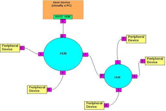
USB connectors: connecting a USB device to a computer is very simple. You find the USB connector on the back of your machine and plug to USB connector into it. If it is a new device, the operating system auto detect set and asks for the driver desk. If the device has already been installed, the computer activates it and starts talking to it. The USB standard specifies two kinds of cables and connectors, as shown below. The USB standard uses A and B connectors mainly to avoid confusion: A connectors head upstream towards the computer, B connectors, head down streams and connect to individual devices. By using different connectors on the upstream and downstream end, it is impossible to install a cable incorrectly, because the two types are physically different.

USB can support for data transfer types or transfer mobiles. Control isochronous bulk interrupt. Next paragraph. Control transfers, exchange configuration setup, and command information between the device and host. The host can also send commands or query parameters, with control packets. Isochronous transfer is used. My time Critical commerce streaming device. Such a speakers, video cameras. It s time sensitive information. So, within limitations, it has guaranteed access to the USB. Bulk transfer is used by devices like printers and scanners, which receives data in one big packet. Interrupt transfer, is used by peripherals exchanging small amount of data that need immediate attention. All USB data send serial. USB data transfer is essential in the form of packets of data commerce send back and forth between the host and peripheral devices. Initially, all packets are sent from the host, via the root hub and possibly more hubs, to devices. Each USB data transfer consists of
1. Token packet
2. Optional Data Packet
3. Statis Packet
Timer
- A device, which counts the input at regular interval (T) using clock pulses at its input.
- The counts increment on each pulse
- Store in a register, called count register
- Output bits (in a count register or at the output pins) for the present counts.
Evaluation of Time
- The counts multiplied by the interval T give the time.
- The (present counts initial counts) T interval gives the time interval between two instances when present count bits are read and initial counts were read or set.
Timer
- Has an input pin (or a control bit in control register) for resetting it for all count bits = 0s.
- Has an output pin (or a status bit in status register) for output when all count bits = 0s after reaching the maximum value, which also means after timeout or overflow.
Counter
- A device, which counts the input due to the events at irregular or regular intervals.
- The count gives the number of input events or pulses since it was last read.
- Has a register to enable read of present counts
- Functions as timer when counting regular interval clock pulses
- Has an input pin (or a control bit in control register) for resetting it for all count bits = 0s.
- Has an output pin (or a status bit in status register) for output when all count bits = 0s after reaching the maximum value, which also means after timeout or overflow.
Timer or Counter Interrupt
When a timer or counter becomes 0x00 or 0x0000 after 0xFF or 0xFFFF (maximum value), it can generate an ‘interrupt’, or an output ‘Time-Out’ or set a status bit ‘TOV’.
Free running Counter (Blind running Counter)
- A counting device may be a free running (blind counting) device giving overflow interrupts at fixed intervals.
- A pre-scalar for the clock input pulses to fix the intervals.
Free Running Counter
It is useful
- For action or initiating chain of actions
- Processor interrupts at the preset instances
- Noting the instances of occurrences of the events
- Processor interrupts for requesting the processor to use the capturing of counts at the input instance
- Comparing of counts on the events for future actions
Free running (blind counting) device Many Applications Based on
- Comparing the count (instance) with the one preloaded in a compare register [an additional register for defining an instance for an action]
- Capturing counts (instance) in an additional register on an input event. [An addition input pin for sensing an event and saving the counts at the instance of event and taking action.]
Free running (Blind Counts) input OC enable pin (or a control bit in control register)
- For enabling an output when all count bits at free running count = preloaded counts in the compare register.
- At that instance a status bit or output pin also sets in and an interrupt ‘OCINT’ of processor can occur for event of comparison equality.
- Generates alarm or processor interrupts at the preset times or after preset interval from another event
Free running (Blind Counts) input capture -enable pin (or a control bit in control register) for Instance of Event Capture
- A register for capturing the counts on an instance of an input (0 to 1 or 1 to 0 or toggling) transition
- A status bit can also set in and processor interrupt can occur for the capture event
Free running (Blind Counts) Pre-scaling
- Prescalar can be programmed as p = 1, 2, 4, 8, 16, 32, .. By programming a prescaler register. Prescalar divides the input pulses as per the programmed value of p.
- Count interval = p T interval
- T = clock pulses period, clock frequency = T1
Free running (Blind Counts) Overflow
- It has an output pin (or a status bit in status register) for output when all count bits = 0s after reaching the maximum value, which also means after timeout or overflow
- Free running n-bit counter overflows after p 2n T interval
Uses of Timer/Counter Related Devices
- Real Time Clock Ticks (System Heart Beats). [Real time clock is a clock, which, once the system starts, does not stop and can't be reset and its count value can't be reloaded. Real time endlessly flows and never returns back!] Real Time Clock is set for ticks using prescaling bits (or rate set bits) in appropriate control registers.
- Initiating an event after a preset delay time. Delay is as per count value loaded.
Use of Timer Devices
- Initiating an event (or a pair of events or a chain of events) after a comparison(s) with between the pre-set time(s) with counted value(s). [It is similar to a preset alarm(s).]
- A preset time is loaded in a Compare Register. [It is similar to presetting an alarm].
- Capturing the count value at the timer on an event. The information of time (instance of the event) is thus stored at the capture register.
- Finding the time interval between two events. Counts are captured at each event in capture register(s) and read. The intervals are thus found out.
- Wait for a message from a queue or mailbox or semaphore for a preset time when using RTOS. There is a A predefined waiting period is done before RTOS lets a task run.
- Watchdog timer. It resets the system after a defined time.
- Baud or Bit Rate Control for serial communication on a line or network. Timer timeout interrupts define the time of each baud
- Input pulse counting when using a timer, which is ticked by giving nonperiodic inputs instead of the clock inputs. The timer acts as a counter if, in place of clock inputs, the inputs are given to the timer for each instance to be counted.
- Scheduling of various tasks
- A chain of software-timers interrupt and RTOS uses these interrupts to schedule the tasks.
- Time slicing of various tasks. A multitasking or multi-programmed operating system presents the illusion that multiple tasks or programs are running simultaneously by switching between programs very rapidly, for example, after every 16.6 ms.
- Process known as a context switch. [RTOS switches after preset time-delay from one running task to the next. Task. Each task can therefore run in predefined slots of time]
- Time division multiplexing (TDM)
- Timer device used for multiplexing the input from a number of channels.
- Each channel input allotted a distinct and fixed-time slot to get a TDM output. [For example, multiple telephone calls are the inputs and TDM device generates the TDM output for launching it into the optical fiber.
Timer States
- Reset State (initial count = 0)
- Initial Load State (initial count loaded)
- Present State (counting or idle or before start or after overflow or overrun)
- Overflow State (count received to make count = 0 after reaching the maximum count)
- Overrun State (several counts received after reaching the overflow state)
- Running (Active) or Stop (Blocked) state
- Finished (Done) state (stopped after a preset time interval or timeout)
- Reset enabled/disabled State (enabled resetting of count = 0 by an input)
- Load enabled/disabled State (reset count = initial count after the timeout)
- Auto Re-Load enabled/disabled State (enabled count = initial count after the timeout)
- Service Routine Execution enable/disable State (enabled after timeout or overflow)
Software timer
- A timer which executes a software after the counts increment by certain pre-defined value and interrupt from to a system and executes a set of software instructions (ISR)
- The software timer which generates interrupt on overflow of count-value or on finishing value of the count variable and runs a set of instructions (ISR).
System clock
- A hardware-timing device programmed to tick at constant intervals T.
- An interrupt at each tick
- A chain of interrupts thus occurs at periodic intervals.
- T is as per a preset count value
- The interrupts are called system clock interrupts, when used to control the schedules and timings in the system
- System clock has fixed program to tick at constant intervals T.
- SWTs have fixed but programmable to tick at intervals T.
- An interrupt at each tick in both
- The interrupts called system clock and SWT interrupts, respectively
Watchdog timer is a hardware microcontroller. It is basically used to take out a system from an infinite loop and resets the system. Watchdog makes the embedded systems more reliable as it works as a safety mechanism.
Watchdog is a type of counter. It is an up counter which means that it counts from zero and reaches to some values. As soon the watchdog timer reaches some value its hardware generates a watchdog reset. Then the system resets this count value to zero in order to avoid system reset. The watchdog timer is loaded with some values which are based on its timeout time. The system needs to reset the counter before timeout.
Watchdog Timer Hardware
The figure below is of watchdog time hardware with input as clock. With every clock the internal counter increments. Then the comparator will compare this value with the loaded count value. Then if the comparator finds that count value matches the watchdog hardware generates and resets it.

Watchdog in Microcontroller MSPXXX Family
The internal watchdog of the MSP430 family is used either as a simple timer or as a watchdog that ensures system integrity. The watchdog function is enabled after power-on reset or system reset. In case of any difficulties after start-up of MSP430, the watchdog will reset the system as often as it is needed for it to start successfully.
A system running with MCLK = 3 MHz uses the watchdog for supervision of three functions.
Power Fail — by checking the 60 Hz AC line.
Function 1 — A check is made if the software reaches this background part regularly
Function 3 — A check is made if this interrupt handler is called regularly.
Each supervised function sets a dedicated bit in RAM byte WDB in intervals less than 10.66 ms (power-up value of the watchdog with MCLK = 3 MHz) if everything is functioning normally.
The main loop checks this byte (WDB) and resets the watchdog ONLY if all three bits are set (07h). If one of the functions fails, the watchdog is not reset and will therefore reset the system.
Real time clock
Features:
- Real-time clock (RTC) counts seconds, minutes, hours, date of the month, month, day of the week, and year with leap-year compensation valid up to 2100
- 56-byte, battery-backed, non-volatile (NV) RAM for data storage
- Two-wire serial interface
- Programmable square wave output signal
- Automatic power-fail detect and switch circuitry
- Consumes less than 500nA in battery backup mode with oscillator running
- Optional industrial temperature range: -40°C to +85°C

Fig 10. DS 1307 Pin Diagram
Device Addressing
DS 1307 requires 8-bit device word follwing the start condition.
To enable the chip to read or write operation.

The device address word consists of a mandatory zero seequence for MSB as shown.
RTC and RAM address map

The address map for the RTC and RAM registers of the DS1307 are shown, The RTC registers are in address locations
Ooh to 07h. The RAM registers are in address locations 08h to 3Fh. During a multi-byte access, when the address pointer reaches 3Fh, the end of RAM space, it wraps around to location Ooh, the beginning of the clock space.
RTC clock

Write Operation:

- Serial data and clock are received through SDA and SCL.
- After each byte is received an acknowledge bit is transmitted.
- START and STOP conditions are recognized as the beginning and end of a serial transfer. Hardware performs address recognition after reception of the slave address and direction bit (see Figure).
- The slave address byte is the first byte received after the master generates the START condition.
- The slave address byte contains the 7-bit DS1307 address, which is 1101000, followed by the direction bit (R/W), which for a write is 0.
- After receiving and decoding the slave address byte, the DS1307 outputs an acknowledge on SDA. After the DS1307 acknowledges the slave address + write bit, the master transmits a word address to the DS1307.
- This sets the register pointer on the DS1307, with the DS1307 acknowledging the transfer.
- The master can then transmit zero or more bytes of data with the DS1307 acknowledging each byte received.
- The register pointer automatically increments after each data byte are written.
- The master will generate a STOP condition to terminate the data write.
Read Operation:
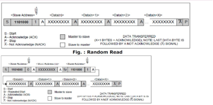
Fig 11. Write memory pointer
- The first byte is received and handled as in the slave receiver mode. However, in this mode, the direction bit will indicate that the transfer direction is reversed.
- The DS1307 transmits serial data on SDA while the serial clock is input on SCL.
- START and STOP conditions are recognized as the beginning and end of a serial transfer (see Figure).
- The slave address byte is the first byte received after the START condition is generated by the master. The slave address byte contains the 7-bit DS1307 address, which is 1101000, followed by the direction bit (R/W), which is 1 for a read.
- After receiving and decoding the slave address the DS1307 outputs an acknowledge on SDA.
- The DS1307 then begins to transmit data starting with the register address pointed to by the register pointer. If the register pointer is not written to before the initiation of a read mode the first address that is read is the last one stored in the register pointer.
- The register pointer automatically increments after each byte are read.
- The DS1307 must receive a Not Acknowledge to end a read.
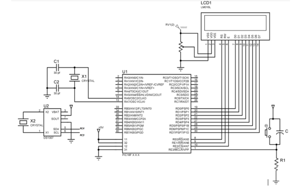
Figure 12. Interfacing
Key takeaway
- After each byte is received an acknowledge bit is transmitted.
- START and STOP conditions are recognized as the beginning and end of a serial transfer. Hardware performs address recognition after reception of the slave address and direction bit (see Figure).
- The slave address byte is the first byte received after the master generates the START condition.
- The slave address byte contains the 7-bit DS1307 address, which is 1101000, followed by the direction bit (R/W), which for a write is 0.
References:
1. M. A. Mazidi, J. G. Mazidi and R. D. McKinlay, “The8051Microcontroller and Embedded Systems:
Using Assembly and C”, Pearson Education, 2007.
2. K. J. Ayala, “8051 Microcontroller”, Delmar Cengage Learning,2004.
3. The 8051 Microcontroller Based Embedded System By Manish K. Patel TMH.
4. Embedded System Architecture, Programming and Design by Raj Kamal, 3rd Edition TMH.
5. Introduction to Embedded System by Shibu K. V. 3rd Edition TMH