Unit 4
Semiconductor physics
In an isolated atom, the electrons are tightly bound and have discrete, sharp energy levels [Figure]. When two identical atoms are brought closer, the outermost orbits of these atoms overlap and interact. When the wave functions of the electrons of the different atoms begin to overlap considerably, the energy levels split into two
If more atoms are bought together, more levels are formed and for a solid of N atoms, each of the energy levels of an atom splits into N levels of energy [Figure]. The levels are so close together that they form an almost continuous band. The width of this band depends on the degree of overlap of the electrons of adjacent atoms and is largest for the outermost atomic electrons. In a solid, many atoms are brought together that the split energy levels form a set of energy bands of very closely spaced levels with forbidden energy gaps between them. Overlapping of these atoms occurs for smaller equilibrium spacing.
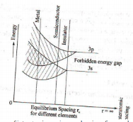
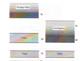
The band corresponding to outermost orbit is called conduction band and the next band is called valence band. The gap between these two allowed bands is called forbidden energy gap or band gap. According to the width of the gap between the bands and band occupation by electrons all solids can be classified broadly into three groups namely, conductors, semiconductors and insulators.
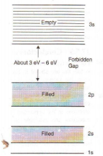
On the basis of band theory, solids can be broadly classified into three categories, viz, insulators, semiconductors and conductors. Their band structures can be as follow:
Insulators
1. In case of insulators, the forbidden gap is very wide. Due to this fact electrons cannot jump from valence band to conduction band.
2. They have completely filled valence band and completely empty conduction band.
3. The resistivity of insulators is very high.
4. Insulators are bad conductors of electricity.
Semiconductors.
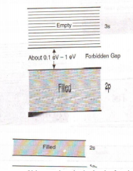
1. In semiconductors, the band gap is very small (0.7 eV for germanium and 1.1 eV for silicon).
2. At 0k, these are no electrons in the conduction band and the valence band is completely filled. As the temperature increases, electrons from the valence band jump into conduction band.
3. The resistivity varies from 10 -14 to 107Ω meter.
4. They have electrical properties between those of insulators and conductors
Conductors
1. In case of conductors, there is no forbidden gap and the valence band conduction band overlaps each other.
2. Plenty of free electrons are available for electrical conduction.
3. They possess very low resistivity and very high conductivity values.
4. Metals c like copper, iron etc. are best examples of conductors
When the material is at a temperature higher than OK, it receives thermal energy from surroundings i.e. electrons are thermally excited. As a result, they move into the higher energy levels which are unoccupied at OK. The occupation obeys a statistical distribution called Fermi – Dirac distribution law.
According to this distribution law, the probability F(E) that a given energy state E is occupied at a temperature T is given by

Here F(E) is called Fermi – Dirac probability function. It indicates that the fraction of all energy state (E) occupied under thermal equilibrium ‘K’ is Boltzmann constant.
Fermi Dirac distribution function:
Mathematically the probability of finding an electron in the energy state E at the temperature T is expressed as
Where, is the Boltzmann constant
T is the absolute temperature
Ef is the Fermi level or the Fermi energy
Now, let us try to understand the meaning of Fermi level. In order to accomplish this, put
in equation (1). By doing so, we get,
This means the Fermi level is the level at which one can expect the electron to be present exactly 50% of the time.
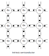
A pure semiconductor is called intrinsic semiconductor. A pure crystal of Germanium and Silicon is an example for intrinsic semiconductor.
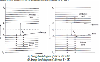
At T=0K, the semiconductor acts as insulator. Germanium and silicon are tetravalent atoms (i.e. four valence electrons) and both have diamond crystal structure. In order to gain stability each germanium atom makes four covalent bonds with the four surrounding germanium atoms by sharing of their valence electrons as shown in figure. At 0K, the semiconductor crystal acts as a perfect insulator since the covalent bonds are strong and no free electrons are available.
At room temperature (T>0K) the semiconductor gives some conductivity since some of the covalent bonds are broken due to the thermal energy supplied to the crystals. The vacancy of an electron in the covalent is called hole. Thus, the valence band has holes and conduction band has electrons For silicon energy gap is 1.12eV and for germanium energy gap is 0.7eV. In intrinsic semiconductor the electron concentration is equal to the hole concentration. In intrinsic semiconductors Fermi level is always lies between valence band and conduction band.
Fermi level in intrinsic semiconductor
In intrinsic semiconductor n = p
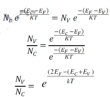
Taking log both side
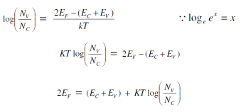

We assume that Nc=Nv
0 
This is the fermi level in intrinsic semiconductor


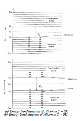

The conductivity of an intrinsic semiconductor can be increased by adding small amounts of impurity atoms, such as III rd or Vth group atoms. The conductivity of silica is increased by 1000 times on adding 10 parts of boron per million part of silicon. The process of adding impurities is called doping and the impurity added is called dopant.
N – Type semiconductor
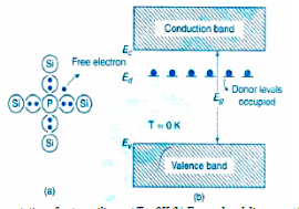
In a pure (intrinsic) semiconductor, when pentavalent an impurity like Phosphorous atom consisting of five valance electrons is doped, and then concentration of electrons increases than holes. Hence the given semiconductor formed is called N – type semiconductor. This is shown in the figure 7a below. By adding donor impurities, the free electrons generated or donated, form an energy level called as “Donor energy level” i.e. ED is shown in the figure below.
P- type semiconductor
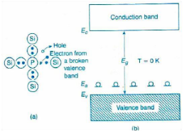
P – Type semiconductor is formed by doping with trivalent impurity atoms (acceptor) like III rd group atoms i.e. Aluminum, Gallium, and Indium etc to a pure semiconductor like Ge or Si. As the acceptor trivalent atoms has only three valance electrons & Germanium , Silicon has four valence electrons; holes or vacancy is created for each acceptor dopant atom. Hence holes are majority and electrons are minority. It is shown in the figure a below. Also an acceptor energy level „EA‟ is formed near VB consisting of holes, as shown in the figure below.
In case of semiconductors we observe two kinds of currents
- Drift current
- Diffusion current
Drift current
The flow of electric current due to the motion of charge carriers under the
Influence of external electric field is called drift current.
When an electric field E is applied across a semiconductor material, the charge
Carriers attain a drift velocity vd.
So, drift velocity
Vd=µE----------------(1)
The relation between current density J and drift velocity vd is
J=Nqvd
Where N is the carrier concentration
q is the charge of electron or hole
From equations (1) and (2), we get

_ is the mobility of charge carrier.
The above equation shows the general expression for drift current density.
Drift current density due to electrons is

Where is the electrons carrier concentration and
µe the mobility of electrons
Drift current density due to holes is

T Total drift current density:

Diffusion current:
The flow of electric current due to the motion of charge carriers under concentration
Gradient is called diffusion current
Or
The motion of charge carriers from the region of higher concentration to lower
Concentration leads to a current called diffusion current.
Let be the excess electron concentration. Then according to Fick’s law, the rate of
Diffusion of charge carriers is proportional to concentration gradient is

Hence
Rate of diffusion of charge:

Where D is the diffusion coefficient of charge carriers
The negative sign indicates decrease of N with increase of x
So, the diffusion current density Jdiffu is:

The expression for total current density due to electrons is

When a layer of P - type semiconducting material is placed with a layer of N- type semiconducting material in such a way that the atoms of P-type combine with the atoms of N-type across the surface of contact, such a surface junction where combination has occurred is known as PN junction.
Combined p-type and n-type semiconductors with PN junction formation is known a junction diode or PN diode
Biased pn junction diode by diffusion technique:
Diffused junctions are formed by impurity diffusion technique. The diffusion process employs either gas diffusion method or solid diffusion method for example in gas diffusion method a wafer of n-type silicon is heated at about 10000 c in a gaseous atmosphere of high concentration gradient the boron atoms.
At the temperature due to concentration gradient the boron atom diffuse in to silicon forming p-n junction in solid diffusion process a p-type impurity (say indium) is painted on a n-type substrate and both are heated. Now impurity atoms diffuse into n-type substrate for a short distance and form p-n junction.

*The formation PN junction is represented in a figure. Let us consider the formation of a sharp junction when two separate semiconductors of p and n type are brought together.
* The p-type has holes as majority carriers and electrons as minority carriers while n-type has electrons as majority carries and holes as minority carriers.
* When they are joined, in the region of contact the free electrons diffuse from n-region and combine with holes in p-region. This leaves n-region near the boundary positively charged and p-region negatively as a result, electric field EB appears in a small region W on either side of the junction O. This region is called “Depletion region “. The thickness of this region is in the older of 6 ×10⁻⁶ cm.
* Due to electric field E B potential difference appears across the depletion region and this potential VB is called “Contact Potential or Barrier Potential or Junction Barrier”.
Energy Band Diagram of PN Diode:
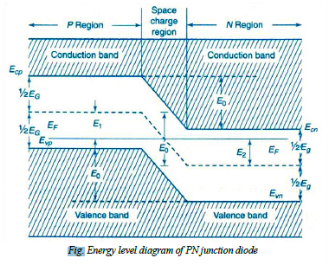
The contact potential VB across the junction is due to the potentials of depletion region on n- side denoted by vn and p – side denoted by vp
i.e.: VB = Vn - Vp → (7)
The energy levels of valance band, conduction band and Fermi level of both p- type and n- type semiconductors. When Pn junction is formed the Fermi, levels become common for both the types formation of potential barrier is represented in fig.
The contact potential separates the energy bands in p—type and n- type crystals. Since there is no net current flow at equilibrium i.e. under unbiased condition, it should have common Fermi level. Hence in PN junction diode the valance and conduction band energy levels Evp and Ecp of p- type and at higher level compared to the valance and conduction band energy levels Evn and Ecn of n-type. The electric field EB across the junction is given by
EB = Evp - Evn = Ecp - Ecn = e VB → (8)
Biased PN Junction:
When the PN junction is unbiased, it is in equilibrium and contact potential VB (= Vn- Vp) appears across the depletion region.
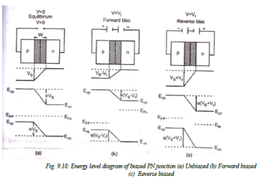
* If now an external voltage is applied across depletion region such that positive of the source is connected to the p-type side and negative of the source is connected to the n-type then junction is said to be “Forward biased”. This voltage Vf appears across the depletion region. As the contact potential difference VB acts from n to p the electrostatic potential barrier is lowered and is given by VB -Vf.
* If the external voltage Vr is applied across the depletion region such that the negative of the source is connected to the p- type side and positive of source is connected to the n- type side then the junction is said to be “Reverse biased :. Since this potential act along VB, the electrostatic potential barrier increases. And is given by VB+Vr. Thus on application of forward bias, the electric field in the transition region reduces and the application of reverse bias increases the electric field in the transition region.
* Since the width of the transition region is propositional to the square root of the electrostatic potential barrier, the width of the transition region decreases under forward bias and increases under reverse bias.
The bipolar transistor has four distinct regions of operation:
– Forward Active
– Reverse Active
– Saturation
– Cutoff
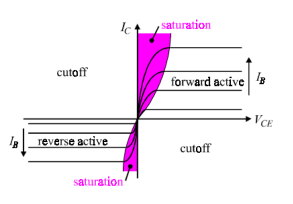
Forward bias:
When the base-emitter junction is forward biased and the base collector junction is reverse biased (implying VCE > VBE), the device is in the forward active region of operation.
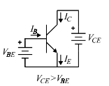
Reverse bias:
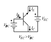
When the base collector junction is forward biased and the base emitter junction is reverse biased (implying VEC > VBC), the device is in the reverse active region of operation
• Basically, the forward active region with roles of emitter and collector reversed
Saturation state:
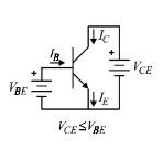
• The saturation region of operation is characterized by forward bias potentials on both the base-emitter and base collector junctions (implying VBE ≥ VCE)
Cut off state:
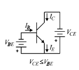
When both junctions are reverse biased (implying VBE negative and VBE ≥ VCE) the device is in the cutoff region of operation
A rectifier is a circuit that converts AC to DC and this conversion process is called rectification. In simple words, a rectifier converts the bi-directional flow of current to a unidirectional flow, which maintains a constant polarity across the load. It can be done by either blocking the reverse flow of current or by redirecting the reverse flow to one direction
Half Wave rectifier
A half wave rectifier clips the negative half cycles and allows only the positive half cycles to flow through the load. Thus it utilizes only the one-half cycle of the input signal.
During the positive half cycle (A- Positive & B- Negative) of the signal, the diode will be forward biased and conducts the current through the load resistance. And on negative half cycle (A- Negative & B- Positive), the diode will be reverse biased and prevents the current to flow in the opposite direction. So the polarity of the output terminals keeps unchanged and obtains a unidirectional current through the load.
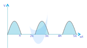
Average voltage, Vaverage = Vm/π | Average Current, I average = Im/π
Rms Voltage, Vrms = Vm/2 | Rms Current, Irms = Im/2
Ripple factor = 1.21
Maximum efficiency = 40.6%
Transformer utilization factor (TUF) = 0.287
Form factor = 1.57
Peak factor = 2
Average voltage,
VDC = Vm/2π 0∫π sinωt dωt
= Vm/2π [ – cosωt]0π = Vm/2π [- cosπ + cos0]
= Vm/2π [1+1] = 2Vm/2π = Vm/π
The RMS voltage, VRMS = √ Vm2/2π 0∫π sin2ωt dωt
= √ Vm2/2π 0 ∫π(1 – cos2ωt) / 2 ) dωt = √ Vm2/4π [ωt – sin2ωt / 2]0π
= √ Vm2/4π [ π – (sinπ) / 2 – (0 – (sin0) / 2)] = √ Vm2/4π ( π ) = √ Vm2/ 4
Therefore, the RMS voltage, VRMS = Vm/ 2
Full Wave rectifier theory
It converts the complete cycles of the AC signal to DC. Both positive and negative half cycles of the AC signal is converted to a unidirectional flow of current.
Full wave center tap rectifier circuit
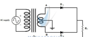
On the positive half cycle (A- Positive & B- Negative), the diode D1 is forward biased and diode D2 is in reverse biased. Hence the current flow through D1 and the load resistance, from terminal A to centre tap.
On the negative half cycle (A- Negative & B- Positive), the diode D2 is forward biased and diode D1 is reverse biased. Current flows through D2 and load resistance, from the B terminal to the centre tap of the transformer.
The biasing of diodes changes alternately with respect to change in the polarity of terminals.
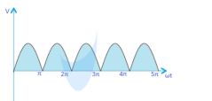
Full wave Rectifier equations and values
Average voltage, Vaverage = 2Vm/π | Average Current, Iaverage = 2Im/π
RMS Voltage, Vrms = Vm/√2 | RMS Current, Irms = Im/√2
Centre tap rectifier, Transformer utilization factor (TUF) = 0.693
Bridge rectifier, Transformer utilization factor (TUF) = 0.812
Ripple factor = 0.482
Maximum efficiency = 81.2%
Form factor = 1.11
Peak factor = √2
Average voltage,
VDC = Vm/π 0∫π sinωt dωt
= Vm/π [ – cosωt]0π = Vm/π [- cosπ + cos0]
= Vm/π [1+1] = 2Vm/π
The RMS voltage,
VRMS = √ Vm2/π 0∫π sin2ωt dωt
= √ Vm2/π 0 ∫π(1 – cos2ωt) / 2 ) dωt = √ Vm2/2π [ωt – sin2ωt / 2]0π
= √ Vm2/2π [ π – (sinπ) / 2 – (0 – (sin0) / 2)] = √ Vm2/2π ( π ) = √ Vm2/ 2
RMS voltage, VRMS = Vm/ √2
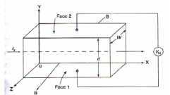
When a material carrying current is subjected to a magnetic field in a direction perpendicular to direction of current, an electric field is developed across the material in a direction perpendicular to both the direction of magnetic field and current direction. This phenomenon is called “Hall-effect”.
Explanation:
* Consider a semi-conductor, and current passes along the X-axis and a magnetic field Bz is applied along the Z-direction, a field Ey is called the Hall field which is developed in the Y-direction.
* In P- type semi-conductor, holes move with the velocity “V” in the “+”ve X-direction. As they move across the semiconductor the holes experience a transverse force ‘Bev’ due to the magnetic field.
* This force drives the holes down to the lower face. As a result, the lower face becomes +vely charged and –ve charge on the upper surface creating the hall field in the Y-direction. The Hall field exerts an upward force on holes equal to Ee.
* In the steady sate, two forces just balance and as a result, no further increase of + ve charge occurs on Face1.
* In N type semiconductor, the majority charge carriers are electrons experiences a force in the downward direction and lower face gets – vely charged. As a result, Hall field will be in the Y – direction.
Hall Coefficient:
Hall field𝐸𝐻, for a given material depends on the current density J and the applied magnetic field B.
i.e. 𝐸𝐻α JB
𝐸𝐻 = 𝑅𝐻 α JB
Since,
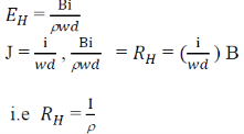
This is called hall coefficient.
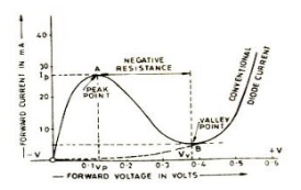
- It immediately conducts the diode when forward biased voltage is applied.
- The current is increases to its peak point value (Ip).
- The diode currents start decreasing till it reaches its minimum value called valley point current (Iv) corresponding to valley voltage (Vv), when the forward voltage is increases. Current starts increasing again as in ordinary junction diode, for more voltage than valley voltage (Vv).
- The region between point A and B is called negative resistance region.
- Current decreases with increase in applied voltage in negative resistance region that is tunnel diode possessing negative resistance region (Rn) in this region.
- Negative resistance of negative resistance region produces power instead of absorbing power. The negative resistance permits oscillations. So, tunnel diode used as a very high frequency oscillator
VI characteristics of Zener diode
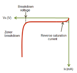
The VI characteristics of a Zener diode is shown in the below figure. When forward biased voltage is applied to the zener diode, it works like a normal diode. However, when reverse biased voltage is applied to the Zener diode, it works in different manner.
When reverse biased voltage is applied to a zener diode, it allows only a small amount of leakage current until the voltage is less than zener voltage. When reverse biased voltage applied to the zener diode reaches zener voltage, it starts allowing large amount of electric current. At this point, a small increase in reverse voltage will rapidly increases the electric current. Because of this sudden rise in electric current, breakdown occurs called zener breakdown. However, zener diode exhibits a controlled breakdown that does damage the device.
The zener breakdown voltage of the zener diode is depends on the amount of doping applied. If the diode is heavily doped, zener breakdown occurs at low reverse voltages. On the other hand, if the diode is lightly doped, the zener breakdown occurs at high reverse voltages. Zener diodes are available with zener voltages in the range of 1.8V to 400V.
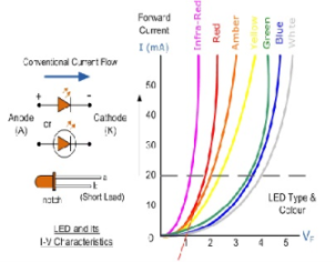
V-I characteristics of LED:
LED is light emitting diode which is heavily doped forward biased p-n junction which convert electric energy into optical energy.
The shorter lead responds to n or cathode side while longer lead corresponds to p or cathode side. The junction is made up of gallium arsenide.
When it is forward biased light photons are emitted from non metallised surface of n region to p region and holes from p to n region. Near junction concentration of minority carrier increases .
On either side the excess minority carriers combine with majority carriers. On recombination energy is released in form of photons. Photons with energy equal or lightly less than band gap are emitted.
As current increases in forward bias intensity of light increases and reaches maximum and further increase in current decreases the light intensity.
For visible spectrum energy gap of semiconductor is from 1.8 eV to 3 eV. The light corresponding to 1.8 eV is red and 3 eV light is violent.
For infrared gap is 1.4 eV.
