Unit - 4
Optical Fiber & Nanoscience
Light propagates inside an optical fiber by virtue of multiple TIRs at the core-cladding interface. The refractive index of the core glass is greater than that of the cladding. This meets the first condition for a TIR. All the light energy that is launched into the optical fiber through its tip does not get guided along the fiber. Only those light rays propagate through the fiber which is launched into the fiber at such an angle that the refracted ray inside the core of the optical fiber is incident on the core-cladding interface at an angle greater than the critical angle of the core with respect to the cladding.
1. Optical fiber is basically a solid glass rod. The diameter of rod is so small that it looks like a fiber.
2. Optical fiber is a dielectric waveguide. The light travels like an electromagnetic wave inside the waveguide. The dielectric waveguide is different from a metallic waveguide which is used at microwave and millimeter wave frequencies.
3. In a metallic waveguide, there is a complete shielding of electromagnetic radiation but in an optical fiber the electromagnetic radiation is not just confined inside the fiber but also extends outside the fiber.
4. The light gets guided inside the structure, through the basic phenomenon of total internal reflection.
5. The optical fiber consists of two concentric cylinders; the inside solid cylinder is called the core and the surrounding shell is called the cladding.
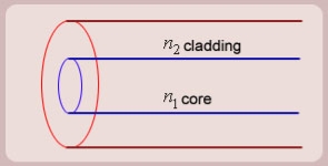
Figure: Schematic of an optical fiber
6. For the light to propagate inside the fiber through total internal reflections at core-cladding interface, the refractive index of the core must be greater than the refractive index of the cladding. That is n1>n2.
Acceptance angle (θ):
It is the maximum angle made by the light ray with the fiber axis, so that light can propagate through the fiber after total internal reflection.
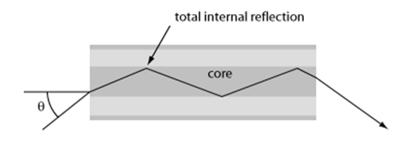
Figure: An incident light ray is first refracted and then undergoes total internal reflection at the core–cladding interface.
Acceptance Cone:
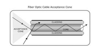
Figure. Acceptance cone.
- The acceptance cone is derived by rotating the acceptance angle about the fiber axis
- The maximum angle, represented in three-dimensional view as a cone, at which an optical fiber will accept incident light.
- Within that cone, as defined by those angles, a light source can inject an optical signal into the fiber core and the signal will remain in the core, reflecting off of the interface between the core and cladding, as illustrated in Figure.
- The angle of acceptance and, therefore, the cone of acceptance are determined by the difference in index of refraction (IOR) between the core and cladding.

Here, ncore and ncladding are the refractive indices of core and cladding, respectively, and n0 is the refractive index of the medium around the fiber, which is close to 1 in case of air.
Numerical Aperture:
Numerical Aperture (NA):It is the light gathering ability or capacity of an optical fiber.NA is related to refractive index of core (n1), cladding (n2) and outside medium (n0) as

Where, n(core) is core refractive index and n(cladding) is cladding refractive index.
Types of Optical Fiber:
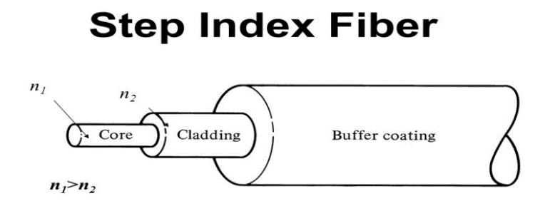
Step index:
They have uniform core with one index of refraction and a uniform cladding with smaller index of refraction. When plotted on the graph as a function of distance from the center of the fiber the index of refraction resembles step-function.
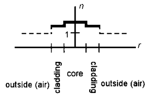
Figure. Step index fiber
- The core of the fiber is the 62 μm-thick clear layer exposed at the right end of the fiber.
- The 125 μm-thick clear layer that comes next is cladding. The next layer is a white protective coating.
- The hair-like insulator allows the fiber to move along its axis, preventing breakage as the fiber is bent and coiled.
- The outer orange coating protects the fiber from environmental effects like moisture.
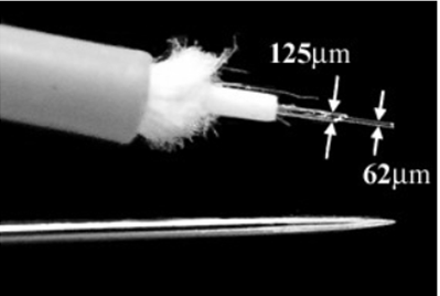
Fig. Construction
Graded index:
Definition:
Graded Index fibre is another type of optical fibre in which the refractive index of the core is non-uniform.
This non-uniformity is present because the refractive index is higher at the axis of the core and continuously reduces with radial movement away from the axis.
However, the refractive index of the cladding is constant in case of graded index fibre. Hence the nature of the refractive index of the core is somewhat parabolic.
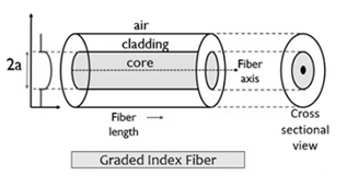
Figure. Graded index
In this type of fibre, the light ray experiences refraction thus gets bent towards the core. Thereby allowing propagation of ray in a curved path.
The refractive index of graded index fibre in the mathematical term is expressed as:

a is the radius of the core
r is the radial distance from the core axis
SIMPLE RAY MODEL

Figure: (optical fiber with core, cladding and total internally reflected ray)
For propagation of light inside the core there are two possibilities.
1. A light ray is launched in a plane containing the axis of the fiber. We can then see the light ray after total internal reflection travels in the same plane i.e., the ray is confined to the plane in which it was launched and never leave the plane. In this situation the rays will always cross the axis of the fiber. These are called the Meridional rays. (Figure 28)
2. The other possibility is that the ray is not launched in a plane containing the axis of the fiber.
For example if the ray is launched at some angle such that it does not intersect the axis of the fiber, then after total internal reflection it will go to some other plane. We can see that in this situation the ray will never intersect the axis of the fiber. The ray essentially will spiral around the axis of fiber. These rays are called the Skew rays.
So it can be concluded that if the light is to propagate inside an optical fiber it could be through two types of rays
a) Meridional rays: The rays which always pass through the axis of fiber giving high optical intensity at the center of the core of the fiber.
b) Skew Rays: The rays which never intersect the axis of the fiber, giving low optical intensity at the center and high intensity towards the rim of the fiber.
Propagation of Meridional Rays
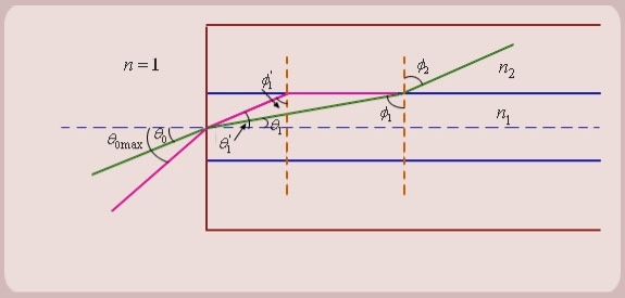
Figure: Propagation of Meridional Rays
1. Let us consider figure. A ray is launched from outside (air) at an angle θ0 , from the axis of the fiber.
The question is, under what conditions the ray is ultimately guided inside the core due to total internal reflections at the core cladding boundary.
2. Let the ray makes an angle θ1 with the axis of the fiber inside the core, and let the ray make an angle ϕ1 with core -cladding interface. Let ϕ2 be the angle of refraction in the cladding.
If ϕ1 < critical angle the ray is refracted in cladding. The ray which goes to cladding is lost and is not useful for communication. The ray which is confined to the core is useful for optical communication.
3. Now as we increase the launching angle θ0, the angle θ1 also increases. Since θ1 + ϕ1 = 
ϕ1 decreases and at some point becomes less than the critical angle. When ϕ1 equals the critical angle, ϕ2 equals  . The maximum launching angle then corresponds to ϕ2 =
 .
.
4. Let us apply Snell’s law at the launching point and at the core-cladding interface for the maximum launching angle θ0max. For this case let θ1 = θ’1 and ϕ1 = ϕ’1
We then have
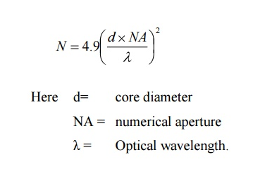
Light propagates as electromagnetic waves through an optical fibre. All waves, having ray directions above the critical angle will be trapped within the fibre due to total internal reflection. However, all such waves do not propagate through the fibre. Only certain ray directions are allowed to propagate. The allowed directions correspond to the modes of the fibre. In simple terms, modes can be visualized as the possible number of paths of light in an optical fibre.
- Single-Mode Fibres:
These fibres are used for long-distance transmission of signals. In general, the single mode fibres are step – index fibres. These types of fibres are made from doped silica. It has a very small core diameter so that it can allow only one mode of propagation and hence called single mode fibres.
The cladding diameter must be very large compared to the core diameter. Thus in the case of single mode fibre, the optical loss is very much reduced. The structure of a single mode fibre is given below.
Structure:
Core diameter : 5-10μm
Cladding diameter : Generally around 125μm
Protective layer : 250 to 1000μm
Numerical aperture : 0.08 to 0.10
Band width : More than 50MHz km.
Application:
Because of high bandwidth, they are used in long haul communication systems.
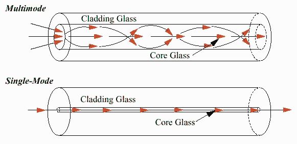
- Multimode Fibres:
These fibres are used for short-distance transmission of signals. The multi-mode fibres are useful in manufacturing both for step – index and graded index fibres. The multi-mode fibres are made by multi-component glass compounds such as Glass – Clad Glass, Silica – Clad – Silica, doped silica etc. Here the core diameter is very large compared to single mode fibres, so that it can allow many modes to propagate through it and hence called as Multi mode fibres. The cladding diameter is also larger than the diameter of the single mode fibres. The structure of the multimode fibre is as shown in the figure above.
Structure:
Core diameter : 50-350μm
Cladding diameter : 125μm - 500μm
Protective layer : 250 to 1100μm
Numerical aperture : 0.12 to 0.5
Band width : Less than 50MHz km.
The total number of modes possible for such an electromagnetic wave guide is

Application:
Because of its less band width it is very useful in short haul communication systems.
Key Takeaways
- Light propagates inside an optical fiber by virtue of multiple TIRs at the core-cladding interface.
- The refractive index of the core glass is greater than that of the cladding.
- Optical fiber is a dielectric waveguide. The light travels like an electromagnetic wave inside the waveguide.
- If the light is to propagate inside an optical fiber it could be through two types of rays; Meridional rays and Skew Rays.
- The quantity
Is called the numerical aperture of an optical fiber. The NA is a measure of the power launching efficiently of an optical fiber. It is given by NA = ( n12- n22 )1/2
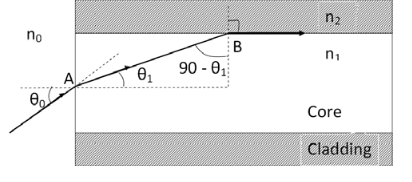
Definition: Acceptance angle is defined as the maximum angle of incidence at the interface of air medium and core medium for which the light ray enters into the core and travels along with the interface of core and cladding.
Let n0 be the refractive indices of air
n1 be the refractive indices of core
n2 be the refractive indices of cladding
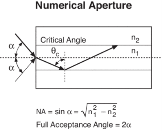
Figure: Acceptance angle
Let a light ray OA is an incident on the interface of air medium and core medium with an angle of incidence θ0
The light ray refracts into the core medium with an angle of refraction θ1 and the refracted ray AB is again incident on the interface of core and cladding with an angle of the incident (90- θ1)
If (90- θ1) is equal to the critical angle of core and cladding media then the ray travels along with the interface of core and cladding along the path BC. If the angle of the incident at the interface of air and core θ1< θ0 then (90- θ1) will be greater than the critical angle. Therefore,
The total internal reflection takes place.
According to Snell’s law at point A
n0 Sin θ0 = n1 Sin θ1
Sin θ0= (n1 / n0) Sin θ1 ………(1)
According to Snell’s law at point B
n1 Sin(90- θ1) = n2 Sin90 ………(2)
n1 Cosθ1 = n2 as (Sin90=1)
Cosθ1 = n2 /n1
Sinθ1 = (1-Cos2 θ1)1/2
Sinθ1= (1- (n2 /n1)2)1/2
Sinθ1= ( n12- n22 )1/2/ n1 ………(3)
We know Sin θ0= (n1 / n0) Sin θ1 from equation (1)
Substitute the value of Sinθ1 from equation (3)
Sinθ0= (n1 / n0) *( n12- n22 )1/2/ n1
On simplification
Sinθ0= ( n12- n22 )1/2/ n0
θ0=Sin-1 ( n12- n22 )1/2/ n0
Acceptance Angle is θ0=Sin-1 ( n12- n22 )1/2/ n0 ………(4)
Definition: -Numerical aperture is defined as the light gathering capacity of an optical fibre and it is directly proportional to the acceptance angle. Numerically it is equal to the sin of the acceptance angle.
NA = Sin(acceptance angle)
NA = Sin {Sin-1 (( n12- n22 )1/2/ n0)} from equation (4)
NA = (( n12- n22 )1/2/ n0) ………(5)
If the refractive index of the air medium is unity i.e. n0=1 put in (5)
NA = ( n12- n22 )1/2 ………(6)
Fractional change in refractive index
∆= (n1- n2)/ n1
n1∆ = (n1- n2) ………(7)
From equation (6), we have
NA = {( n1- n2 )( n1+n2 )}1/2
NA = { n1∆ (n1+n2 )}1/2 as n1∆ = (n1- n2) by Eq(7)
NA = { n1∆ 2n1}1/2 n1 ≈ n2, so n1+n2 =2n1
NA = n1{2∆}1/2
This gives the relation between Numerical aperture and Fractional change in refractive index.

The Numerical Aperture (NA) of a fibre is defined as the sine of the largest angle an incident ray can have for total internal reflectance in the core. Rays launched outside the angle specified by a fibber’s NA will excite radiation modes of the fiber. A higher core index, with respect to the cladding, means larger NA. However, increasing NA causes higher scattering loss from greater concentrations of dopant. A fiber's NA can be determined by measuring the divergence angle of the light cone it emits when all its modes are excited.
Qualitatively, NA is a measure of the light gathering ability of a fiber. It also indicates how easy it is to couple light into a fiber.
Attenuation in Optical Fibres
- Attenuation is a measure of decay of signal strength or loss of light power that occurs as light pulses propagate through the length of the fibre
- In optical fibres the attenuation is mainly caused by two physical factors absorption and scattering losses. Absorption is because of fibre material and scattering due to structural imperfection within the fibre.
- Nearly 90 % of total attenuation is caused by Rayleigh scattering only. Micro bending of optical fibre also contributes to the attenuation of signal.
- The rate at which light is absorbed is dependent on the wavelength of the light and the characteristics of particular glass. Glass is a silicon compound; by adding different additional chemicals to the basic silicon dioxide the optical properties of the glass can be changed.
- The Rayleigh scattering is wavelength dependent and reduces rapidly as the wavelength of the incident radiation increases.
- The attenuation of fibre is governed by the materials from which it is fabricated, the manufacturing process and the refractive index profile chosen.
- Attenuation loss is measured in dB/km.
As attenuation leads to a loss of power along the fibre, the output power is significantly less than the couples power. Let the couples optical power is P(0) i.e. at origin (z =0).Then the power at distance z is given by,
P(z) = P(0) 
Where, αp is fibre attenuation constant (per km).
αp =  ln
ln 
αp (dB/km ) = 10.  log
log 
αp (dB/km ) = 4.343 αp/km
This parameter is known as fibre loss or fibre attenuation. Attenuation is also a function of wavelength.
Example: When mean optical power launched into an 8 km length of fibre is 12 μW, the mean optical power at the fibre output is 3 μW. Determine
a) Overall signal attenuation in dB.
b) The overall signal attenuation for a 10 km optical link using the same fibre with splices at 1 km intervals, each giving an attenuation of 1 dB.
Solution:
Given :z=8km
P(0) = 120 μW
P(z) = 3 μW
a) Overall attenuation is given by,
αp (dB/km ) = 10. log  = 16.02
b) Overall attenuation for 10 km,
Attenuation per km = αp (dB/km )
= 
=  = 2.00 dB/km
Attenuation in 10 km link = 2.00 x 10 = 20 dB
In 10 km link there will be 9 splices at 1 km interval. Each splices introducing attenuation of 1 dB.
Total attenuation = 20 dB + 9 dB = 29 dB
Dispersion in Optical Fibres
Dispersion: A light pulse launched into a fibre decreases in the fibre. It also spreads during its travel. The pulse received at the output is wider than input pulse.
It means that the pulse becomes distorted as it is propagated through the fibre. Such a distortion arises due to dispersion effects.
Dispersion is typically measured in Nano seconds per kilometre (ns/km).
There are three mechanisms which contribute to the distortion of the light pulse in a fibre. They are known as:
- Material dispersion
- Wave guide dispersion
- Intermodal dispersion
- Material Dispersion
Material dispersion is also called as chromatic dispersion. Material dispersion exists due to change in index of refraction for different wavelengths. A light ray contains components of various wavelengths. The time delay is different for different wavelength components. This results in time dispersion of pulse at the receiving end of fibre.
Light waves of different wavelengths travel at different speeds in a medium. The short wavelength waves travel slower than long wavelength waves. Consequently, narrow pulses of light tend to broaden as they travel down the optical fibre. This is known as material dispersion.
The material dispersion for unit length (L = 1) is given by
D = 
Where c = Light velocity
λ = Center wavelength
 = Second derivative of index of refraction w.r.t wavelength.
Negative sign shows that the upper sideband signal (lowest wavelength) arrives before the lower sideband (highest wavelength).
The unit of dispersion is : ps/nm/km. The amount of material dispersion depends upon the chemical composition of glass.
Example: An LED operating at 850 nm has a spectral width of 45 nm. What is the pulse spreading in ns/km due to material dispersion?
Solution:
Given :λ = 850 nm
σ = 45 nm
R.M.S pulse broadening due to material dispersion is given by,
σm= σLM
Considering length L = 1 metre
Dmat = 
For LED source operating at 850 nm,  = 0.025
M =  by substituting all values we have
M = 9.8 ps/nm/km
σm= 441 ns/km
Waveguide Dispersion
- Waveguide dispersion is caused by the difference in the index of refraction between the core and cladding, resulting in a ‘drag’ effect between the core and cladding portions of the power.
- Waveguide dispersion is significant only in fibres carrying fewer than 5-10 modes. Since multimode optical fibres carry hundreds of modes, they will not have observable waveguide dispersion.
- The group delay (τwg) arising due to waveguide dispersion.
τwg =  [ n2 +n2 ∆
  ]
]
Where, b = Normalized propagation
Constant k = 2π / λ (group velocity)
Normalized frequency V,
V = ka 
τwg =  [ n2 +n2 ∆
  ]
]
The second term  is waveguide dispersion and is mode dependent term.
As frequency is a function of wavelength, the group velocity of the energy varies with frequency. This produces additional losses (waveguide dispersion). The propagation constant (b) varies with wavelength, the causes of which are independent of material dispersion.
Chromatic Dispersion
The combination of material dispersion and waveguide dispersion is called chromatic dispersion. These losses primarily concern the spectral width of transmitter and choice of correct wavelength.
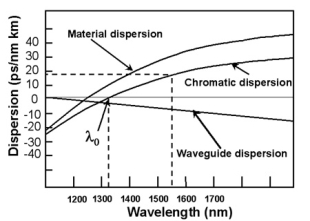
Material dispersion and waveguide dispersion effects vary in opposite senses as the wavelength increased, but at an optimum wavelength, two effects almost cancel each other and chromatic dispersion is at minimum. Attenuation is therefore also at minimum and makes highly attractive Operating wavelength.
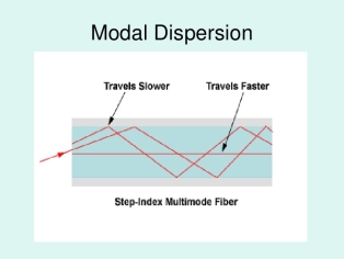
Modal Dispersion
As only a certain number of modes can propagate down the fibre, each of these modes carries the modulation signal and each one is incident on the boundary at a different angle, they will each have their own individual propagation times. The net effect is spreading of pulse; this form o dispersion is called modal dispersion.
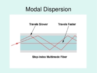
Modal dispersion takes place in multimode fibres. It is moderately present in graded index fibres and almost eliminated in single mode step index fibres.
- Modal dispersion is given by
∆tmodal = 
Where ∆tmodal = Dispersion
n1= Core refractive index
Z = Total fibre length
c = Velocity of light in air.
The above equation can also be written as
∆tmodal = 
The modal dispersion ∆tmodal describes the optical pulse spreading due to modal effects optical pulse width can be converted to electrical rise time through the relationship.
tr mod = 0.44 (∆tmodal)πr2
ADVANTAGES OF FIBRE OPTIC COMMUNICATION
The optical fibre communication has more advantages than convectional communication.
1. Enormous Bandwidth
2. Low Transmission Loss
3. Electric Isolation
4. Signal Security
5. Small Size and Less Weight
6. Immunity Cross Talk
1. Enormous bandwidth:- The information carrying capacity of a transmission system is directly proportional to the frequency of the transmitted signals. In the coaxial cable transmission, the bandwidth range is up to around 500MHz only. Where as in optical fibre communication, the bandwidth range is large as 105 GHZ.
2. Low transmission loss:- The transmission loss is very low in optical fibres (i.e.KmdB/2.0) than compare with the conventional communication system. Hence for long distance communication fibres are preferred.
3. Electric isolation:- Since fibre optic materials are insulators, they do not exhibit earth and interface problems. Hence communicate through fibre even in electrically danger environment.
4. Signal security:- The transmitted signal through the fibre does not radiate, unlike the copper cables, a transmitted signal cannot be drawn from fibre without tampering it. Thus the optical fibre communication provides 100% signal security.
5. Small size and less weight:- The size of the fibre ranges from 10μm to 50μm, which is very small. The space occupied by the fibre cable is negligibly small compared to conventional electrical cables. Optical fibres are light in weight.
6. Immunity cross talk:- Since the optical fibres are dielectric wave guides, they are free from any electromagnetic interference and radio frequency interference. Since optical interference among different fibres is not possible, cross talk is negligible even many fibres are cabled together.
DISADVANTAGES OF OPTICAL FIBRE
The disadvantages of optical fibre include the following
- The main disadvantages of these cables are installation is expensive and difficult to fix together.
- The optical fibre cables are very difficult to merge & there will be a loss of the beam within the cable while scattering.
- Fibre optic cables are compact and highly vulnerable while fitting
- These cables are more delicate than copper wires.
- Special devices are needed to check the transmission of fibre cable.
APPLICATION OF OPTICAL FIBRE
- Optical fibres are extensively used in communication system.
- Optical fibres are in exchange of information between different computers
- Optical fibres are used for exchange of information in cable televisions, space vehicles, submarines etc.
- Optical fibres are used in industry in security alarm systems, process control and industrial auto machine.
- Optical fibres are used in pressure sensors in biomedical and engine control.
- Optical fibres are used in medicine, in the fabrication in endoscopy for the visualization of internal parts of the human body.
- Sensing applications of optical fibres are Displacement sensor, Fluid level detector, Liquid level sensor, Temperature/pressure sensor and Chemical sensors
- Medical applications of optical fibres are Gastroscopy, Orthoscopic, Couldoscope, Peritonescope and Fibrescope.
The basic building blocks of an optical-fibre link are the light source, the fibre and the detector.

Figure: An optical-fibre link
There are broadly speaking two categories of device used as light sources: light-emitting diodes (LEDs) and laser diodes. In general terms, LEDs are cheaper and easier to use, but have inferior performance compared to laser diodes.
The output from an LED differs from that of a laser diode as it is possible to couple more light power from a laser diode than from an LED to an optical fibre, and the spectral linewidth of an LED is much broader than that of a laser diode.
i) Temperature Sensor
A temperature sensor is a device that detects and measures hotness and coolness and converts it into an electrical signal. At TE Connectivity (TE), we design and manufacture a broad portfolio of temperature sensors – including our NTC thermistors, RTDs, thermocouples, and thermopiles – designed for efficiency and easy installation, with capacity to reliably integrate technology that responds to human behavior.
Ii) Pollution / Smoke detector
Air pollution sensors are devices that monitor the presence of air pollution in the surrounding area. They can be used for both indoor and outdoor environments. These sensors can be built at home, or bought from certain manufactures. Although there are various types of air pollution sensors, and some are specialized in certain aspects, the majority focuses on five components: ozone, particulate matter, carbon monoxide, sulfur dioxide, and nitrous oxide. The sensors were very expensive in the past, but with technological advancements these sensors are becoming more affordable and more widespread throughout the population. These sensors can help serve many purposes and help bring attention to environmental issues beyond the scope of the human eye.
Inside any building and home, fire alarm and smoke detectors systems are vital safety feature. They becoming more sophisticated, incorporating more sensors to detect not only smoke and fire but also monitoring the quality of the air. These devices can alert individuals and authorities quicker, reducing the alert time and avoid property damage and casualties and they are dependent on very low power as high power means higher costs and more frequent maintenance both in a residential home and in a commercial building.
Iii) Liquid level sensor
Liquid level sensors, also called liquid level switches, are designed to change state when immersed in a liquid. They are used to determine if a liquid or oil exists at a particular level in a container.
The different kinds of liquid level sensors include
- Optical
- Capacitive
- Conductive
- Diaphragm
- Float
1. Optical Liquid Level Sensors
Optical sensors work by are solid state. They use an infra-red LED and phototransistor which are optically coupled when the sensor is in air. When the sensing tip is immersed in liquid, the infra-red light escapes making the output change state. These sensors can detect the presence or absence of almost any liquid. They are not sensitive to ambient light and are not affected by foam when in air or by small bubbles when in liquid. This makes them useful where the state change must be quickly and dependably noted, and where they can function reliably for extended periods without maintenance.
For example, the SST Optomax Digital Liquid Level Sensor is a popular low-cost, low-maintenance infra-red LED sensor.
The disadvantage of an optical liquid level sensor is that it can only determine if liquid is present or not present. If variable levels are required, (25%, 50%, 100%, etc.) each requires an additional sensor.
2. Capacitive Liquid Level Sensors
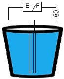
Capacitive liquid level switches use 2 conductive electrodes (usually made of metal) in a circuit that are a short distance from each other. When the electrodes are immersed in a liquid it completes a circuit.
The advantage of a capacitive liquid level switch is that it can be used to determine the rising or falling of liquid in a container. By making the electrodes the same height as the container, the capacitance between the electrodes can be measured. No capacitance means no liquid. Full capacitance means a full container. Both “empty” and “full” measurements must be recorded, then a meter calibrated with 0% and 100% to show the liquid level.
Although capacitive liquid level sensors have the advantage of no moving parts, one of their disadvantages is that corrosion of the electrodes will change the electrode’s capacitance requiring either cleaning or recalibration. They are also more sensitive to the type of liquid used.
3. Conductive Liquid Level Sensors

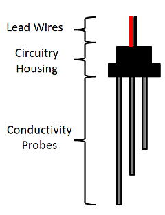
Conductive liquid level switches are sensors with an electrical contact at a specific liquid level. Two or more insulated electrodes with exposed tips are used inside a pipe lowered into the liquid. A longer electrode carries a low voltage, while a shorter one is used to complete the circuit when the liquid level rises to meet it.
Like capacitive liquid level switches, conductive liquid level switches depend on the conductivity of the liquid. Therefore, they are only useful for measuring certain types of liquids. In addition, these sensors tips must be cleaned at regular intervals to reduce fouling.
4. Diaphragm Liquid Level Sensors
Diaphragm or pneumatic liquid level switches rely on air pressure to push a diaphragm which engages a micro-switch inside the body of the unit. As the liquid level rises, the internal pressure inside a detecting pipe rises until the micro-switch or a pressure sensor is activated. As the liquid level falls, the air pressure also falls and the switch is disengaged.
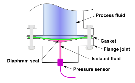
The advantage of a diaphragm-based liquid level switch is that no power source inside the tank is required, it can be used with many types of liquids, and since the switch does not come in contact with the liquid. However, because it is a mechanical device, over time it will require maintenance.
5. Float Liquid Level Sensors

Float switches are the original liquid level sensors. They are mechanical devices. A hollow float is connected to an arm. As the float rises and falls in the liquid, the arm is pushed up and down. The arm may be connected to a magnetic or mechanical switch to determine on/off, or it may be connected to a gauge that rises from full to empty as the liquid levels falls.
The ball float switch in a toilet tank is the most common type of float liquid level sensor used. Sump pumps also use float switches (see right) as a cost-effective way to measure the water level in a basement sump pit.
Float switches can measure any type of liquid, and can be designed to require no power to operate. The disadvantage of float switches is that they are larger than other types of switches and because they are mechanical, must be services more often than other liquid level switches.
i) PIN detector
An optical detector is a device that converts light signals into electrical signals, which can then be amplified and processed. The photodetector is as essential an element of any fiber optic system as the optical fiber or the light source. Photodetectors can dictate the performance of a fiber optic communication link.
Semiconductor Photodiodes
Semiconductor photodiodes are the most commonly used detectors in optical fiber systems since they provide good performance, being small in size, and are of low cost.
Semiconductor photodiodes are made of silicon, germanium, GaAs, InGaAs, etc.
How Does a Photodetector Work?
The following illustration shows how a photodetector work. The detector is electrically reverse-biased. (In contrary, LEDs and Lasers are forward-biased to emit light).
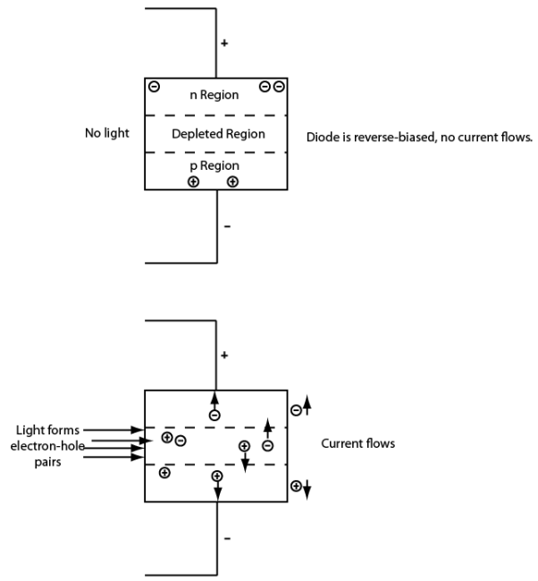
In the first illustration when there is no light, the reverse bias draws current-carrying electrons and holes out of the p-n junction region, creating a depleted region, which stops current from passing through the diode.
In the second illustration when there are lights on the detector, photons with the proper energy (wavelength) can create electron-hole pairs in this region by raising an electron from the valence band to the conduction band, leaving a hole behind. The bias voltage causes these current carriers to drift quickly away from the junction region, so a current flows proportional to the light hitting the detector.
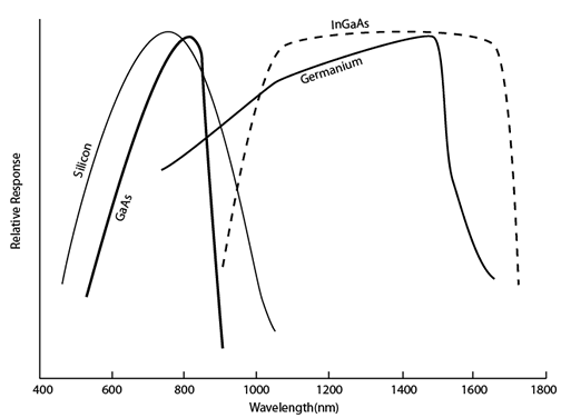
The wavelengths at which the detector responds to light depend on the detector’s material composition.
Photodetector Response Curves
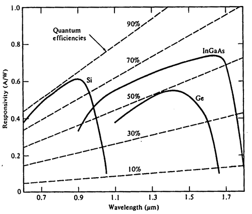
As we said above, the wavelength that a photodetector can respond to depends on its composition. The following graph shows the detector response curve for different materials.
PIN Photodetector
The most common semiconductor photodetector is the PIN photodiode as shown below.
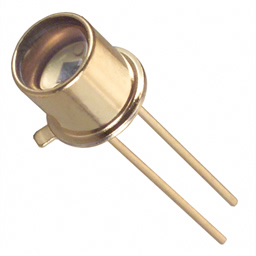
PIN photodiode has an intrinsic (very lightly doped) semiconductor region sandwiched between a p-doped and an n-doped region (as shown below).
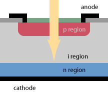
The PIN photodiode is reverse-biased as shown above. Since the intrinsic (i) region has no free charges, its resistance is high, so that most of the reverse-biased voltage is applied to this i region.
The i region is usually wide so that incoming photons have a greater probability of absorption in the i region rather than in the p or n regions.
Since the electric field is high in the i region, any electron-hole pairs generated in this region are immediately swept away by the field. e-h pairs generated in the p and n regions have to first diffuse into the depletion region before being swept away. Also, these e-h pairs may suffer recombination, resulting in a reduced current.
PIN Photodetector Characteristics
1. Quantum Efficiency
Sensitivity measures the response to an optical input signal as a function of its intensity. Photodetector’s sensitivity can be measured in two concepts: quantum efficiency and responsivity.
We will focus on quantum efficiency in this section, and we will introduce responsivity in the next section.
Quantum efficiency
η measures the fraction of incoming photons that generate electrons at the detector. It is defined as

Quantum efficiency
η is the ratio of the number of electron-hole (e-h) pairs generated to the number of incident photons. It can by calculated by

Where
R is the reflection coefficient at the air-semiconductor surface
ξ is the fraction of the e-h pairs contributes to the photo current
α is the absorption coefficient
ω is the distance where optical power is absorbed
2. Responsivity
Responsivity is the ratio of electrical output from the detector to the input optical power. If the output current varies proportionally to the input, this is measured as amps per watt (A/W). Since in fiber optic communication systems, input powers are usually in microwatt level, responsivity is often expressed as uA/uW.
The responsivity ρ is the photo current generated per unit optical power. The following formula shows how to calculate responsivity.

Where
λ0 is measured in um (micrometers)
η is the quantum efficiency
The following figure shows the spectral dependence of responsivity and quantum efficiency for different semiconductor materials.
3. Speed of Response and Bandwidth
The speed of response and bandwidth of a photodetector depend on three factors.
- The transit time of the photo-generated carriers through the depletion region
- The electrical frequency response as determined by the RC time constant, which depends on the diode’s capacitance
- The slow diffusion of carriers generated outside the depletion region
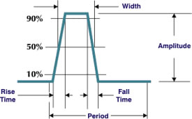
Rise Time
Rise time is the time the output signal takes to rise from 10% to 90% of the peak value after the input is turned on instantaneously.
Fall Time
Fall time is the the time the output signal takes to drop from 90% to 10% of the peak value after the input is turned off abruptly.
Photodetector Bandwidth
Detector bandwidth usually is defined as the frequency at which the output signal has dropped to 3dB (50%) below the power at a low frequency. This means that only half as much signal is getting through the detector at the higher frequency.
In a square wave function, the highest frequencies are responsible for the sharp edges. Frequencies higher than the bandwidth frequency (50%) are attenuated even more. As bandwidth decreases, the pulses become more rounded.
4. Dark Current
Dark current is the current through the photodiode in the absence of light, when it is operated in photoconductive mode. The dark current includes photocurrent generated by background radiation and the saturation current of the semiconductor junction.
Dark current sets a floor on the minimum detectable signal, because a signal must produce more current than the dark current in order to be detected. Dark current depends on operating temperature, bias voltage, and the type of detector.
Dark current must be accounted for by calibration if a photodiode is used to make an accurate optical power measurement, and it is also a source of noise when a photodiode is used in an optical communication system.
5. Noise-Equivalent Power (NEP)
Noise-Equivalent Power (NEP) is the minimum input optical power to generate photocurrent, equal to the rms noise current in a 1 hertz bandwidth.
This more directly measures the minimum detectable signal because it compares noise directly to optical power.
NEP depends on the frequency of the modulated signal, the bandwidth over which noise is measured, the detector area, and the operating temperature.
6. Table of Typical Performance Characteristics of Detectors
Parameter | Silicon | Germanium | InGaAs | |||
PIN | APD | PIN | APD | PIN | APD | |
Wavelength range (nm) | 400 – 1100 | 800 – 1800 | 900 – 1700 | |||
Peak (nm) | 900 | 830 | 1550 | 1300 | 1300 (1550) | 1300 (1550) |
Responsivity | 0.6 | 77-130 | 0.65-0.7 | 3-28 | 0.63-0.8 (0.75-0.97) |
|
Quantum Efficiency (%) | 65 – 90 | 77 | 50-55 | 55-75 | 60-70 | 60-70 |
Gain (M) | 1 | 150-250 | 1 | 5-40 | 1 | 10-30 |
Excess Noise Factor (x) | – | 0.3-0.5 | – | 0.95-1 | – | 0.7 |
Bias Voltage (-V) | 45-100 | 220 | 6-10 | 20-35 | 5 | <30 |
Dark Current (nA) | 1-10 | 0.1-1.0 | 50-500 | 10-500 | 1-20 | 1-5 |
Capacitance (pF) | 1.2-3 | 1.3-2 | 2-5 | 2-5 | 0.5-2 | 0.5 |
Rise Time (ns) | 0.5-1 | 0.1-2 | 0.1-0.5 | 0.5-0.8 | 0.06-0.5 | 0.1-0.5 |
Ii) Avalanche Detector
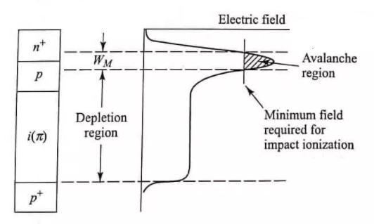
It internally multiply the primary signal photocurrent before it enters the input circuitry of the following amplifier. This increases receiver sensitivity, since the photocurrent is multiplied before encountering the thermal noise associated with the receiver circuit. In order for carrier multiplication to take place, the photogenerated carriers must traverse a region where a very high electric field is present. In this high-field region, a photogenerated electron or hole can gain enough energy so that it ionizes bound electrons in the valence band upon colliding with them. This carrier multiplication mechanism is known as impact ionization. The newly created carriers are also accelerated by the high electric field, thus gaining enough energy to cause further impact ionization. This phenomenon is the avalanche effect. Below the diode breakdown voltage a finite total number of carriers are created, whereas above breakdown the number can be infinite.
A commonly used structure for achieving carrier multiplication with very little excess noise is the reach through construction 14-16 shown in blow image. The reach-through avalanche photodiode (RAPD) is composed of a high-resistivity p-type material deposited as an epitaxial layer on a pt (heavily doped p-type) substrate. A p-type diffusion or ion implant is then made in the high-resistivity material, followed by the construction of an nt (heavily doped n-type) layer. For silicon, the dopants used to form these layers are normally boron and phosphorus, respectively. This configuration is referred to as p+ πpn+ reach-through structure. The 7 layer is basically an intrinsic material that inadvertently has some p doping because of imperfect purification. Blow describes more complex structures used for InGaAs APDs.

Fig.: Avalanche Detector
Introduction to nanoscience
The word Nanoscience refers to the study, manipulation and engineering of matter, particles and structures on the nanometer scale (one millionth of a millimeter, the scale of atoms and molecules). Important properties of materials, such as the electrical, optical, thermal and mechanical properties, are determined by the way molecules and atoms assemble on the nanoscale into larger structures. Moreover, in nanometer size structures these properties often different then on macroscale, because quantum mechanical effects become important.
Introduction to nanotechnology
While the word Nano technology is relatively new, the existence of nanostructures and Nano devices is not new. Such structures existed on the earth as life itself began though it is not known when humans to use nanosized materials the first known, Roman glassmakers were fabricated glasses containing nanosized metals. When the material size of the object is reduced to nanoscale, then it exhibits different properties than the same material in bulk form.
The concept and idea of nanotechnology original discussed first time in 1959 by Richard Feynman, the renowned physicist. Richard Feynman in his talk “There's Plenty of Room at the Bottom,” described the feasibility of synthesis via direct manipulation of atoms. However, in 1974, the term "Nano-technology" was first used by Norio Taniguchi.
Nanoscience
Nano science deals with the study of properties of materials at nano scales where properties differ significantly than those at larger scale.
Nanotechnology
Nanotechnology deals with the design, characterization, production and applications of nanostructures and nanodevices and nanosystems.
CHARATERIZATION
Physical properties
Inter atomic distance: When the material size is reduced to Nano scale, surface area to volume ratio increases. Due to increase of surface of surface area, more number of atoms will appear at the surface of compared to those inside. So Interatomic spacing decreases with size.
Thermal properties: Nano materials are different from that of bulk materials. The Debye Temperature and ferroelectric phase transition temperature are lower for nano materials. The melting point of nano gold decreases from 1200 K to 800K as the size of particle decreases form 300 Å to 200 Å.
Optical properties: Different sized nano particles scatters different of light incident on it and hence they appear with different colours. For example nano gold does not act as bulk gold. The nano particles of gold appear as orange, purple, red or greenish in colour depending on their grain size. The bulk copper is opaque whereas nanoparticle copper is transparent.
Magnetic properties: The magnetic properties of nano materials are different from that of bulk materials. In explaining the magnetic behaviour of nanomaterials, we use single domains unlike large number of domains in bulk materials. The coercivity value of single domain is very large.
For example, Fe, Co, and Ni are ferromagnetic in bulk but they exhibit super par magnetism. Na, K, and Rh are paramagnetic in bulk but they exhibit ferro-magnetic. Cr is anti-ferromagnetic in bulk but they exhibit super paramagnetic.
Mechanical properties: The mechanical properties such as hardness, toughness, elastic modulus, young’s modulus etc., of nano materials are different from that of bulk materials. In metals and alloys, the hardness and toughness are increased by reducing the size of the nano particles. In ceramics, ductility and super plasticity are increased on reducing grain size. Hardness increases 4 to 6 times as one goes from bulk Cu to nanocrystalline and it is 7 to 8 times for Ni.
Chemical properties
Nanocrystalline materials are strong, hard, erosion and corrosion resistant. They are chemically active and have the following chemical properties.
- In electrochemical reactions, the rate of increase in mass transport increases as the particle size decreases.
- The equilibrium vapour pressure, chemical potentials and solubilites of nanoparticles are greater than that for the same bulk material.
- Most of the metals do not absorb hydrogen. But the hydrogen absorption increases with the decrease of cluster size in Ni, Pt and Pd metals.
Basic principles of nanomaterials
When the material size of the object is reduced to nanoscale, then it exhibits different properties than the same material in bulk form. The factors that differentiate the nanomaterials from bulk material is
- Increase in surface area to volume ratio
- Quantum confinement effect
Increase in surface area to volume ratio: The ratio of surface area to volume ratio is large for nano materials.
Example 1: To understand this let us consider a spherical material of radius ‘r’. Then its surface area to volume ratio is 3/r. Due to decrease of r, the ratio increases predominantly.
Example 2: For one cubic volume, the surface ratio is 6m2. When it is divided into eight cubes its surface area becomes 12m2. When it is divided into 27 cubes its surface area becomes 18m2. Thus, when the given volume is divided into smaller pieces the surface area increases.
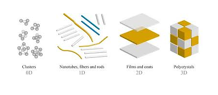
Figure: Surface area to volume ratio
Due to increase of surface of surface area, more number of atoms will appear at the surface of compared to those inside. For example, a nano material of size 10nm has 20% of its atoms on its surface and 3nm has 50% of its atoms. This makes the nanomaterials more chemically reactive and affects the properties of nano materials.
Quantum confinement effect: According to band theory, the solid atoms have energy bands and isolated atoms possess discrete energy levels. Nano materials are the intermediate state to solids and atoms. When the material size is reduced to nanoscale, the energy levels of electrons change. This effect is called quantum confinement effect. This affects the optical, electrical and magnetic properties of nanomaterials.
All materials are composed of grains. The visibility of grains depends on their size. Convectional materials have grains varying in size from hundreds of microns to millimetres. The materials processing grains size ranging from 1 to 100 nm, known as Nano materials. Nano materials can be produced in different dimensionalities.
- One dimensional nano material: Surface coatings and thin films
- Two-dimensional nano materials: nano tubes nano wires, biopolymers
- Three-dimensional nano materials: nano particles, precipitates, colloids, quantum dots, nano crystalline materials, fullerenes or carbon nano-60.
Classification of nanostructured materials
In the past two decades, hundreds of novel NSMs (nanostructured materials) have been obtained therefore, the need in their classification become important.
NSMs as a subject of nanotechnology are low dimensional materials comprising of building units of a submicron or nanoscale size at least in one direction and exhibiting size effects.
The first classification idea of NSMs was given by Gleiter in 1995 and further was explained by Skorokhod in 2000. However, Gleiter and Skorokhod scheme was not fully considered because of 0D, 1D, 2D, and 3D structures such as fullerenes, nanotubes, and nanoflowers were not taken into account.
After them Pokropivny and Skorokhod reported a modified classification scheme for NSMs, in which 0D, 1D, 2D and 3D NSMs are included.
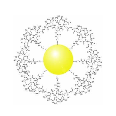
Figure: Classification of nanostructured materials
0D Nanostructured Materials
In the past 10 years, significant progress has been made in the field of 0D NSMs. 0D NSMs such as uniform particles arrays (quantum dots), heterogeneous particles arrays, core–shell quantum dots, onions, hollow spheres and nanolenses have been synthesized by several research groups. 0D NSMs, such as quantum dots has been extensively studied in light emitting diodes (LEDs), solar cells, single-electron transistors, and lasers.
A 0D structure is the simplest block that can be used for the design of nanomaterials. In this case, the three dimensions are in the nanometre regime and have a diameter less than 100 nm. Nanoparticles, nanocrystals, and nanoclusters correspond to this group.
Nanoparticles
They are nanostructures usually used to define all 0D nanostructures or those that are amorphous and have an irregular shape. So, the nanoparticles can be of natural origin, semiconductor, metal, oxides, fullerenes or quantum dots.
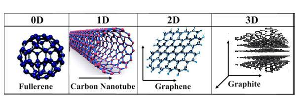
Figure: Nanoparticle
During manufacturing, the nanoparticles that make up the nanomaterials can be of different sizes, which can vary by more than 15% and still form the nanomaterial without affecting its design. 3D nanomaterials should not be included in the category of nanostructures unless their internal structure is nanostructured.
Nanoclusters
As well as the nanoparticles, they have an irregular structure besides being semi crystalline, but they are tinier than the nanoparticles. Its diameter ranges between 1 and 10 nm.
Also nanoclusters are sensitive to their size and become more reactive if they increase or decrease proportionally.
Nanocrystals
They are monocrystalline nanostructures, whose size ranges from 1 to 30 nm. Semiconductor nanocrystals are more commonly known as quantum dots.
- One-dimensional nanomaterials (1D)
In the last decade, 1D NSMs have stimulated an increasing interest due to their importance in research and developments and have a wide range of potential applications. It is generally accepted that 1D NSMs are ideal systems for exploring a large number of novel phenomena at the nanoscale and investigating the size and dimensionality dependence of functional properties.
They are also expected to play an important role as both interconnects and the key units in fabricating electronic, optoelectronic, and EEDs with nanoscale dimensions. The field of 1D NSMs such as nanotubes has attained a significant attention. 1D NSMs have a profound impact in nanoelectronics, nanodevices and systems, nanocomposite materials, alternative energy resources and national security. We show the 1D NSMs, such as nanowires, nanorods, nanotubes, nanobelts, nanoribbons, and hierarchical nanostructures, which have been synthesized in the laboratories. They have a variable length, conserving two dimensions (height and width) in the nanometer regime; to these correspond the nanowires and nanotubes.
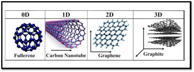
Figure: Classification of nanostructured materials
Nanowires
They are elongated crystalline structures whose characteristics stand out for their conductive or semiconducting properties. Nanowires have been obtained from various metallic materials, semiconductors, oxides, etc. In recent years, nanowires have shown special scientific interest due to their potential applications in nanoelectronics, optoelectronics, and sensors.
Nanotubes
They are tubular structures with a hollow interior. There are nanotubes synthesized and characterized from inorganic laminar materials. However, the most studied are carbon nanotubes (CNT's).
- Two-dimensional nanomaterials (2D)
2D nanostructures have two dimensions outside of the nanometric size range. In recent years, a synthesis 2D NSMs have become a focal area in materials research, owing to their many low dimensional characteristics different from the bulk properties. In the search of 2D NSMs, considerable re-search attention has been focused over the past few years on the development of 2D NSMs. 2DNSMs with certain geometries exhibit unique shape-dependent characteristics and subsequent utilization as building blocks for the key components of nanodevices.
In addition, a 2D NSMs are particularly interesting not only for basic understanding of the mechanism of nanostructure growth, but also for investigation and developing novel applications in sensors, photo catalysts, nano-containers, nanoreactors, and templates for 2D structures of other materials.
There are 2D NSMs such as junctions (continuous islands), branched structures, nanoprisms, nanoplates, nanosheets, nanowalls, and nanodisks.
They are basically nanomaterials formed by very thin layers; thin nanolayers with areas of undefined size and a thickness between 1 and 100 nm.
Graphene is the most notable example because, due to its multiple and exceptional properties, it has the potential to revolutionize technology. Its possible applications extend to very diverse areas, ranging from the miniaturization of electronic devices to the elaboration of drugs against cancer in medicine.
Key Takeaways
- Nanotechnology deals with the design, characterization, production and applications of nanostructures and nanodevices and Nano systems.
- Nano science deals with the study of properties of materials at nano scales where properties differ significantly than those at larger scale.
- When the material size of the object is reduced to nanoscale, then it exhibits different properties than the same material in bulk form.
- Nano materials can be produced in different dimensionalities.
- One dimensional nano material: Surface coatings and thin films
- Two-dimensional nano materials: nano tubes nano wires, biopolymers
- Three-dimensional nano materials: nano particles, precipitates, colloids, quantum dots, nano crystalline materials, fullerenes or carbon nano-60.
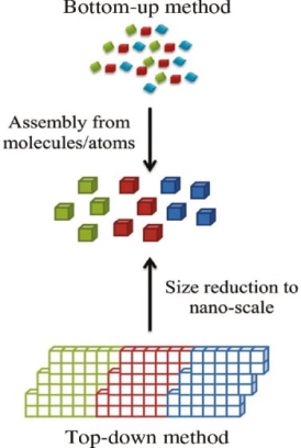
- The methods of producing nanoparticles are classified into two main categories: Bottom-up approach & Top-down approach
The synthesis of nanomaterials is key to the future success of this new technology. The methods of producing nanoparticles are classified into two main categories:
- Top-down approach
- Bottom-up Approach
In bottom-up approaches nanomaterials are assembled from basic building blocks, such as molecules or nanoclusters. The basic building blocks, in general, are nanoscale objects with suitable properties that can be grown from elemental precursors. The concept of the bottom-up approach is that the complexity of nanoscale components should reside in their self-assembled internal structure, requiring as little intervention as possible in their fabrication from the macroscopic world.
The bottom-up approach uses atomic or molecular feed-stocks as the source of the material to be chemically transformed into larger nanoparticles. This has the advantage of being potentially much more convenient than the top-down approach. By controlling the chemical reactions and the environment of the growing nanoparticle, then the size, shape and composition of the nanoparticles may all be affected. For this reason, nanoparticles produced by bottom up, chemically based and designed, reactions are normally seen as being of higher quality and having greater potential applications. This has led to the growth of a host of common bottom-up strategies for the synthesis of nanoparticles. Many of these techniques can be tailored to be performed in gas, liquid, solid states, hence the applicability of bottom-up strategies to a wide range of end products. Most of the bottom-up strategies requires suitable organometallic complexes or metal salts to be used as chemical precursors, which are decomposed in a controlled manner resulting in particle nucleation and growth. One of the key differences that can be used to subdivide these strategies into different categories is the method by which the precursor is decomposed.
A typical example of bottom-up is processing for nanocomposite magnets from individual high-magnetization and high-coercivity nanoparticles. The assembling critically depends on availability of anisotropic (single crystal) hard magnetic nanoparticles. Anisotropic nanoparticles produced via surfactant-assisted high energy ball milling satisfy the major requirements for this application.
Top-down Approach
In top-down approaches, a bulk material is restructured (i.e. partially dismantled, machined, processed or deposited) to form nanomaterials. The aggressive scaling of electronic integrated circuits in recent years can be considered the greatest success of this paradigm. For top-down methods, the challenges increase as devices size is reduced and as the desired component designs become larger and more complex. Also, the top-down assembly of nanocomponents over large areas is difficult and expensive.
The top-down method involves the systematic breakdown of a bulk material into smaller units using some form of grinding mechanism. This is beneficial and simple to execute and avoids the use of volatile and poisonous compounds frequently found in the bottom-up techniques. However, the quality of the nanoparticles formed by grinding is accepted to be poor in comparison with the material produced by modern bottom-up methods. The main drawbacks include defect problems from grinding equipment, low particle surface areas, asymmetrical shape and size distributions and high energy needed to produce relatively small particles. Apart from these disadvantages, it must be distinguished that the nano-material produced from grinding still finds use, due to the simplicity of its manufacture, in applications including magnetic, catalytic and structural properties.
Physical Vapour Deposition
Physical Vapor Deposition (PVD) is fundamentally a vaporization coating technique, involving the transfer of material on an atomic level. The process is similar to chemical vapor deposition (CVD) except that the raw materials/precursors, i.e. the material that is going to be deposited starts out in solid form. In contrast, in CVD, the precursors are introduced to the reaction chamber in the gaseous state.
In PVD, the coating material is evaporated by various mechanisms: resistance heating, electron gun or high-energy ionized gas bombardment and the vapor phase is transported to the substrate, forming a coating as shown in Fig
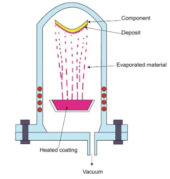
Fig.: PVD process
The PVD process take place between temperatures of 100–600 °C. The variants of PVD process are Sputtering and Electron beam PVD. Major advantage of PVD coatings are: hardness, wear resistance, and improved oxidation resistance. The major disadvantages are: difficult to coat undercuts and similar surface features, high capital cost, and rate of deposition is quite slow.
Sol gel method
The sol–gel method is considered effective to modify the surface of substrates. Obtaining of a high surface area and stable surfaces is the most important advantage of the sol–gel method. The chemical and physical properties of the materials obtained by the sol–gel method are related to the experimental conditions applied. The sol–gel method involves two main reactions: (1) hydrolysis of the precursor in the acidic or basic mediums and (2) polycondensation of the hydrolyzed products. In this way a polymeric network is formed in which MNPs can be retained.
It provides a new approach to the preparation of new materials. This process allows a better control of the whole reactions involved during the synthesis of solids. Homogenous multi-component systems can be easily obtained, particularly homogenous mixed oxides can be prepared by mixing the molecular precursors solutions.
The chemistry of the sol-gel process is basedon hydrolysis and polycondensation reactions. Metal alcoxides [M(OR)3] are versatile molecular used to obtain oxides, on account of their ability to form homogeneous solution in large variety of solvents and in the presence of other alcoxides or metallic derivatives and also for their reactivity toward nucleophilic reagents such as water.
The essential aim for the most investigations reported was the final product and its applications without interested to the synthesis conditions and reactional mechanism involved to obtain gels, although the properties of a gel and its behaviour on heat treatment could be very sensitive to the structure already created during the sol stage. Therefore, the formation of colloidal aggregates determines the main properties of resulting powder. By varying the chemical conditions under which materials is polymerized, the structure and the morphology of samples formed are drastically affected. However, many earlier investigations try to develop a good understanding of gelification phenomenon. The purpose of this work is to better understand the chemistry involved during the preparation of mixed oxides by Sol-gel process, in order to have a good control of the properties of the final material.
Nanomaterials are particles that have their size in 1-100 nm range at least in one dimension. There are different sources of these particles. For example, we can get these particles as engineered particles, as incidental components and via natural sources. There are several forms of nanomaterials;
- Nanomaterials – They have all their dimensions in 1-100 nm scale.
- One dimensional nanostructure – one dimension has its size outside the nanoscale.
- Two-dimensional nanostructures – two of the dimensions are not in nanoscale.
- Bulk nanostructures – none of the dimensions is in the nanoscale (all are above 100 nm).
There are many applications of these materials in various manufacturing processes, healthcare applications, various products including paints, filters, lubricant additives, etc. For example, nanozymes are substances that are nanoparticles, and they have enzyme-like characteristics.
Bulk materials are particles that have their size above 100 nm in all dimensions. Most of the times, we use this term in order to name a substance that is granular or lumpy and exists in free-flowing form. We use the grain size and grain distribution in characterizing these materials. Moreover, we can explain their properties using the bulk density, moisture content, temperature, etc. There are two forms of these materials as follows:
- Cohesionless, free-flowing bulk materials
- Cohesive bulk materials
Bulk materials include the material we use in the construction field; plaster, sand, gravel, cement, etc. Moreover, it includes raw materials that we use for various industries such as ore, slag, salts, etc. In addition to that, this includes powdery materials such as pigments, fillers, granules, pellets, etc.
Zeolites
- Zeolites and mesoporous silica nanoparticles are silicate or aluminosilicate nanomaterials with well-defined pore networks.
- Zeolites are widely used in industry for applications such as catalysis, separations and gas adsorption. Mesoporous silica nanomaterials have not been as extensively applied relative to zeolites due to the cost and reduced thermal stability, but are being intensively investigated for potential environmental and biomedical applications.
- Zeolite and mesoporous silica nanomaterials are reviewed with emphasis on connections to the environment.
- Environmental applications including the adsorption of environmental contaminants and environmental catalysis will also be presented. Finally, the toxicity of zeolite and mesoporous silica nanomaterials will be considered.
Graphine
- Graphene has emerged as one of the most promising nanomaterials because of its unique combination of exceptional properties: it is not only the thinnest but also one of the strongest materials; it conducts heat better than all other materials; it is an excellent conductor of electricity; it is optically transparent, yet so dense that it is impermeable to gases – not even helium, the smallest gas atom, can pass through it.
- Graphene's unique combination of extraordinary properties offers a fascinating material platform for the development of next-generation technologies in many areas – wearable and superfast electronics, ultrasensitive sensors, multifunctional composites and coatings, membranes, medicine nd biotechnology, energy harvesting and storage.
- Graphene is the name for a single layer (monolayer) sheet of carbon atoms that are bonded together in a repeating pattern of hexagons. This sheet is only one atom thick. Monolayers of graphene stacked on top of each other form graphite. Since a typical carbon atom has a diameter of about 0.33 nanometers, there are about 3 million layers of graphene in a 1 mm thick sheet of graphite.
- In scientific terms: The extraordinary characteristics of graphene originate from the 2p orbitals, which form the π state bands that delocalize over the sheet of carbons that constitute graphene.
- Harder than diamond yet more elastic than rubber; tougher than steel yet lighter than aluminum – graphene is the strongest known material.
- To put this in perspective: if a sheet of cling film (like kitchen wrap film) had the same strength as a pristine single layer of graphene, it would require the force exerted by a mass of 2,000 kg, or a large car, to puncture it with a pencil.
- Its high electron mobility is 100x faster than silicon; it conducts heat 2x better than diamond; its electrical conductivity is 13x better than copper; it absorbs only 2.3% of reflecting light; it is impervious so that even the smallest atom (helium) can't pass through a defect-free monolayer graphene sheet; and its high surface area of 2,630 square meters per gram means that with less than 3 grams you could cover an entire soccer field (well, practically speaking you would need 6 grams, since 2,630 m2/g is the surface area for both sides of a graphene sheet).
- Graphene represents a conceptually new class of materials that are only one atom thick, so-called two-dimensional (2D) materials (they are called 2D because they extend in only two dimensions: length and width; as the material is only one atom thick, the third dimension, height, is considered to be zero). And it is only at this single- or few-layer state that graphene’s amazing properties appear.
- Graphene is the basic building block for other graphitic materials like carbon nanotubes.
Nano materials possess unique and beneficial, physical, chemical and mechanical properties; they can be used for a wide verity of applications.
Material technology
- Nanocrystalline aerogel are light weight and porous, so they are used for insulation in offices homes, etc.
- Cutting tools made of Nano crystalline materials are much harder, much more wear- resistance, and last stranger.
- Nano crystalline material sensors are used for smoke detectors, ice detectors on air craft wings, etc.
- Nano crystalline materials are used for high energy density storage batteries.
- Nano sized titanium dioxide and zinc dioxide is used in sunscreens to absorb and reflect ultraviolet rays.
- Nano coating of highly activated titanium dioxide acts as water repellent and antibacterial.
- The hardness of metals can be predominately enhanced by using nanoparticles.
- Nanoparticles in paints change colour in response to change in temperature or chemical environment, and reduce the infrared absorption and heat loss.
- Nano crystalline ceramics are used in automotive industry as high strength springs, ball bearings and valve lifters.
Information technology
- Nanoscale fabricated magnetic materials are used in data storage
- Nano computer chips reduce the size of the computer.
- Nano crystalline starting light emitting phosphors are used for flat panel displays.
- Nanoparticles are used for information storage.
- Nanophotonic crystals are used in chemical optical computers.
Biomedical
- Bio sensitive nanomaterials are used for ragging of DNA and DNA chips.
- In the medical field, nanomaterials are used for disease diagnosis, drug delivery and molecular imaging.
- Nano crystalline silicon carbide is used for artificial heart valves due to its low weight and high strength.
Energy storage
- Nanoparticles are used hydrogen storage.
- Nano particles are used in magnetic refrigeration.
- Metal nanoparticles are useful in fabrication of ionic batteries.
- Nano materials possess unique and beneficial, physical, chemical and mechanical properties; they can be used for a wide verity of applications.
Material technology
- Nanocrystalline aerogel are light weight and porous, so they are used for insulation in offices homes, etc.
- Cutting tools made of Nano crystalline materials are much harder, much more wear- resistance, and last stranger.
- Nano crystalline material sensors are used for smoke detectors, ice detectors on air craft wings, etc.
- Nano crystalline materials are used for high energy density storage batteries.
- Nano sized titanium dioxide and zinc dioxide is used in sunscreens to absorb and reflect ultraviolet rays.
- Nano coating of highly activated titanium dioxide acts as water repellent and antibacterial.
- The hardness of metals can be predominately enhanced by using nanoparticles.
- Nanoparticles in paints change colour in response to change in temperature or chemical environment, and reduce the infrared absorption and heat loss.
- Nano crystalline ceramics are used in automotive industry as high strength springs, ball bearings and valve lifters.
Information technology
- Nanoscale fabricated magnetic materials are used in data storage
- Nano computer chips reduce the size of the computer.
- Nano crystalline starting light emitting phosphors are used for flat panel displays.
- Nanoparticles are used for information storage.
- Nanophotonic crystals are used in chemical optical computers.
Biomedical
- Bio sensitive nanomaterials are used for ragging of DNA and DNA chips.
- In the medical field, nanomaterials are used for disease diagnosis, drug delivery and molecular imaging.
- Nano crystalline silicon carbide is used for artificial heart valves due to its low weight and high strength.
Energy storage
- Nanoparticles are used hydrogen storage.
- Nano particles are used in magnetic refrigeration.
- Metal nanoparticles are useful in fabrication of ionic batteries
Nanotechnology can greatly help in recyclability of waste and packaging, and the development of materials which can be assimilated by the environment such as in the development of degradable plastic bags made from corn. Nanotechnology already provides positive impact on the environment and human health
It extends from its medical, ethical, mental, legal and environmental applications, to fields such as engineering, biology, chemistry, computing, materials science, and communications.
References:
- LASERS: Theory and Applications: Thyagarajan K and Ghatak A.K.
- Nanomaterials & Nanotechnologies and Design: M.F.Ashby, Paulo Ferreira and Daniel L.Schodek, Elsevier Publications.
- University Physics: Young and Freedman (Pearson Education).
- Optics: Jenkins and White (Tata Mcgraw Hill)