Unit - 1
Diode Circuits
A P-N Junction Diode is formed by doping one side of a piece of silicon with a P-type dopant (Boron) and the other side with a N-type dopant (phosphorus). Ge can be used instead of Silicon. The P-N junction diode is a two-terminal device. This is the basic construction of the P-N junction diode. It is one of the simplest semiconductor devices as it allows current to flow in only one direction.
ZERO BIASED CONDITION
In this case, no external voltage is applied to the P-N junction diode; and therefore, the electrons diffuse to the P-side and simultaneously holes diffuse towards the N-side through the junction, and then combine with each other. Due to this an electric field is generated by these charge carriers. The electric field opposes further diffusion of charged carriers so that there is no movement in the middle region. This region is known as depletion width or space charge.
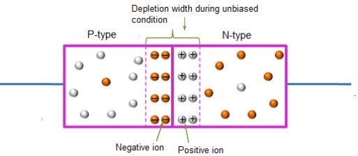
Figure 1: Unbiased or zero biased PN Junction Diode
FORWARD BIAS
In the forward bias condition, the positive terminal of the battery is connected to the P-Type material and the negative terminal of the battery is connected to the N-type material. This connection is also called as giving positive voltage.
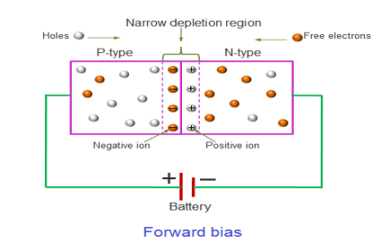
Figure 2: Forward bias
Electrons from the N-region cross the junction and enters the P-region. Due to the attractive force that is generated in the P-region the electrons are attracted and move towards the positive terminal. Simultaneously the holes are attracted to the negative terminal of the battery. By the movement of electrons and holes current flows. In this condition, the width of the depletion region decreases due to the reduction in the number of positive and negative ions.
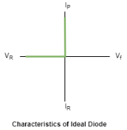
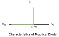
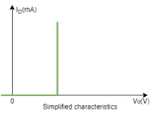
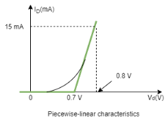
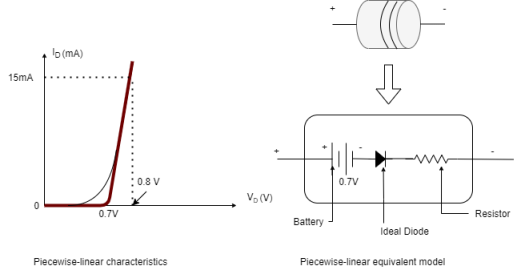
If this external voltage Vf becomes greater than the value of the potential barrier, approx. 0.7 volts for silicon and 0.3 volts for germanium, the potential barriers opposition will be overcome and current will start to flow.
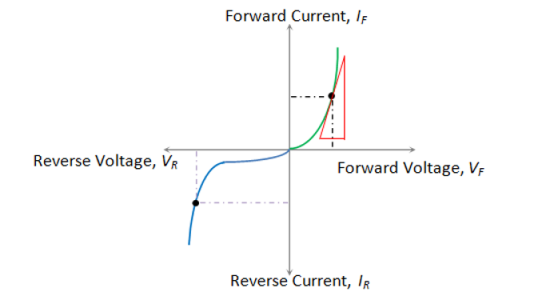
This is because the negative voltage pushes or repels electrons towards the junction giving them the energy to cross over and combine with the holes being pushed in the opposite direction towards the junction by the positive voltage. This results in a characteristics curve of zero current flowing up to this voltage point, called the “knee” on the static curves and then a high current flow through the diode with little increase in the external voltage as shown in I-V characteristics.
REVERSE BIAS
In the reverse bias condition, the negative terminal of the battery is connected to the P-type material and the positive terminal of the battery is connected to the N-type material. This connection is also known as giving negative voltage.
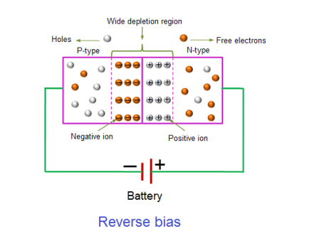
Figure 3: Reverse bias
The positive voltage applied to the N-type material attracts electrons towards the positive electrode and away from the junction, while the holes in the P-type end are also attracted away from the junction towards the negative electrode.
The net result is that the depletion layer grows wider due to a lack of electrons and holes and presents a high impedance path, almost an insulator. The result is that a high potential barrier is created thus preventing current from flowing through the semiconductor material.
This condition represents a high resistance value to the PN junction and practically zero current flows through the junction diode with an increase in bias voltage. However, a very small leakage current does flow through the junction which can be measured in micro-amperes, (μA).
If the reverse bias voltage Vr applied to the diode is increased to a sufficiently high enough value, it will cause the diode’s PN junction to overheat and fail due to the avalanche effect around the junction. This may cause the diode to become shorted and will result in the flow of maximum circuit current, and this shown as a step downward slope in the reverse static characteristics curve in I-V characteristics.
I-V CHARACTERISTICS OF PN JUNCTION DIODE
The I-V Characteristic Curves, which is short for Current-Voltage Characteristic Curves or simply I-V curves of an electrical device
The application of a forward biasing voltage on the junction diode results in the depletion layer becoming very thin and narrow which represents a low impedance path through the junction thereby allowing high currents to flow. The point at which this sudden increase in current takes place is represented on the static I-V characteristics curve above as the “knee” point. The current starts increasing with increase in voltage. At knee voltage current shows a sharp increment in its magnitude. This behaviour is mentioned above. As large current flow in forward biasing so we measure this current in mA.
When a junction diode is Reverse Biased, the thickness of the depletion region increases and the diode acts like an open circuit blocking current flow. So only a very small leakage current will flow.
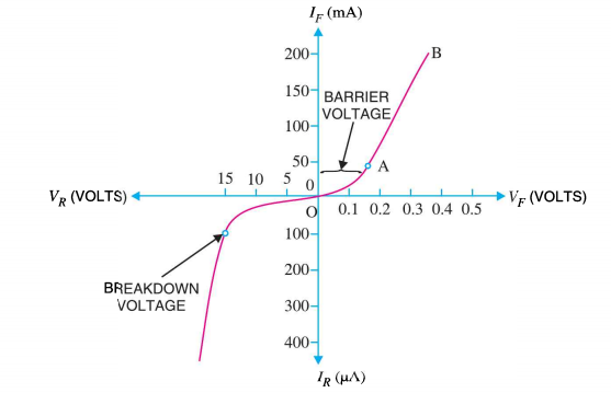
Figure 4: I-V characteristics
Note in addition that the minority carrier drift currents are not affected by the height of the potential bill. It is the number of minority carriers wandering into the depletion region per second that determines the current flow.
The situation is similar to a waterfall. The water flowing over the falls is independent of the height of the falls. The overall 1-V dependence is concluded to be of the general form 1-V characteristics.
 ………. (1)
Equation (1) is identical to the ideal diode equation if VA is set equal to kT/q.
Key Takeaways
A P-N Junction Diode is formed by doping one side of a piece of silicon with a P-type dopant (Boron) and the other side with a N-type dopant (phosphorus). Ge can be used instead of Silicon.
Zero biased condition is the case when no external voltage is applied to the P-N junction diode.
In the forward bias condition, the positive terminal of the battery is connected to the P-Type material and the negative terminal of the battery is connected to the N-type material. This connection is also called as giving positive voltage.
In the reverse bias condition, the negative terminal of the battery is connected to the P-type material and the positive terminal of the battery is connected to the N-type material. This connection is also known as giving negative voltage.
The half-wave rectifier circuit consists of three main parts:
- A transformer
- A resistive load
- A diode
The half wave rectifier is shown in the diagram

Initially a high AC voltage is applied to the to the primary side of the step-down transformer and a low voltage is obtained at the secondary winding which is applied to the diode.

During the positive half cycle of the AC voltage, the diode will be forward biased and the current flows through the diode. During the negative half cycle of the AC voltage, the diode will be reverse biased, and the flow of current will be blocked. The final output voltage waveform on the secondary side (DC) is shown in figure above.
At the secondary side of the circuit, if we replace the secondary transformer coils with a source voltage, we can simplify the circuit diagram of the half-wave rectifier as:
For the positive half cycle of the AC source voltage, the equivalent circuit effectively becomes:
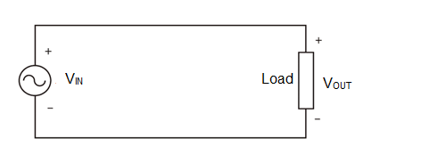
This is because the diode is forward biased and allows current to pass through. Therefore, we have a closed circuit.
For the negative half cycle of the AC source voltage, the equivalent circuit becomes:

Because the diode is now in reverse bias mode, no current will pass through it. Because it is no current can flow through to the load during this time and the output voltage is equal to zero.
Here is what the half wave rectifier waveform looks like on the input side (Vin), and what it looks like on the output side (Vout) after rectification that is conversion from AC to DC.
The graph above actually shows a positive half wave rectifier. This is a half-wave rectifier which only allows the positive half-cycles through the diode, and blocks the negative half-cycle.
Conversely, a negative half-wave rectifier allows negative half-cycles through the diode and will block the positive half-cycle. The only difference between a positive and negative half wave rectifier is the direction of the diode.
Half Wave Rectifier with Capacitor Filter
Filters are components used to convert or smoothen pulsating DC waveforms into constant DC waveforms. This is achieved suppressing the DC ripples in the waveform.
Although half-wave rectifiers without filters are theoretically possible, they cannot be used for any practical applications. As DC equipment requires a constant waveform, we need to ‘smooth out’ this pulsating waveform hence half wave rectifier is used with filter. A capacitor or an inductor can be used as a filter – but half wave rectifier with capacitor filter is mostly used.
The circuit diagram below shows how a capacitive filter is can be used to smoothen out a pulsating DC waveform into a constant DC waveform.
Ripple Factor of Half Wave Rectifier
‘Ripple’ is the unwanted AC component remaining when converting the AC voltage waveform into a DC waveform. Even though we try to remove all AC components, there lies some small amount left on the output side which pulsates the DC waveform. This undesirable AC component is called ‘ripple’.
The ripple factor is the ratio between the RMS value of the AC voltage (on the input side) and the DC voltage (on the output side) of the rectifier.
The formula for ripple factor is:
Ripple factor (γ) = ( I 2 rms – I 2 dc) / Idc = 1.21
Which can also be rearranged to equal:
The ripple factor of half wave rectifier is equal to 1.21 (i.e. γ = 1.21).
Efficiency of Half Wave Rectifier
Rectifier efficiency (η) is the ratio between the output DC power and the input AC power. The formula for the efficiency is equal to:
ղ = Pdc / Pac
The efficiency of a half wave rectifier is equal to 40.6% (i.e. ηmax = 40.6%)
RMS value of Half Wave Rectifier
To derive the RMS value of half wave rectifier, we need to calculate the current across the load.
If the instantaneous load current is equal to iL = Imsinωt, then the average of load current (IDC) is equal to:
Idc = 1/ 2 π sinwt = Im / π
Where Im is equal to the peak instantaneous current across the load (Imax). Hence the output DC current (IDC) obtained across the load is:
Idc = Imax /π where I max = maximum amplitude of dc current
For a half-wave rectifier, the RMS load current (Irms) is equal to the average current (IDC) multiple by π/2. Hence the RMS value of the load current (Irms) for a half wave rectifier is:
I rms = Im /2
Where Im= Imax which is equal to the peak instantaneous current across the load.
Peak Inverse Voltage of Half Wave Rectifier
Peak Inverse Voltage (PIV) is the maximum voltage that the diode can withstand during reverse bias condition. If a voltage is applied more than the PIV, the diode will be destroyed.
Form Factor of Half Wave Rectifier
Form factor (F.F) is the ratio between RMS value and average value, as shown in the formula below:
F.F = RMS value / Average value
The form factor of a half wave rectifier is equal to 1.57 (i.e. F.F= 1.57).
Output DC Voltage
The output voltage (VDC) across the load resistor is denoted by:
VDC = Vs max / π where Vs max = maximum amplitude of secondary voltage.
Applications of Half Wave Rectifier
- For rectification applications
- For signal demodulation applications
- For signal peak applications
Full wave rectifier:
The circuits which convert alternating current (AC) into direct current (DC) are known as rectifiers. If such rectifiers rectify both the positive and negative half cycles of an input alternating waveform, the rectifiers are referred as full wave rectifiers.
A centre-tapped full wave rectifier system consists of:
- Centre-tapped Transformer
- Two Diodes
- Resistive Load
Centre-tapped Transformer: – It is a normal transformer with one slight modification. It has an addition wire connected to the exact centre of the secondary winding. This type of construction divides the AC voltage into two equal and opposite voltages namely +Ve voltage (Va) and -Ve voltage (Vb).
The total output voltage is
V = Va + Vb

Working of Centre-tapped Full Wave Rectifier
We apply an AC voltage to the input transformer. During the positive half-cycle of the AC voltage, terminal 1 will be positive, centre-tap will be at zero potential and terminal 2 will be negative potential. This will lead to forward bias in diode D1 and cause current to flow through it.
During this time, diode D2 is in reverse bias and will block current through it.
During the negative half-cycle of the input AC voltage, terminal 2 will become positive with relative to terminal 2 and centre-tap. This will lead to forward bias in diode D2 and cause current to flow through it. During this time, diode D1 is in reverse bias and will block current through it.
During the positive cycle, diode D1 conducts and during negative cycle diode D2 conducts and during positive cycle. As a result, both half-cycles are allowed to pass through. The average output DC voltage here is almost twice of the DC output voltage of a half wave rectifier.
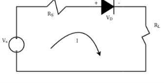
Filter Circuit
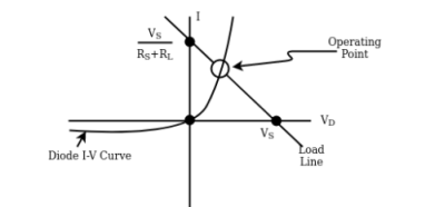
We get a pulsating DC voltage with a lot of ripples as the output of the centre-tapped full wave rectifier.
For practical applications we cannot use this pulsating signal. So, to convert the pulsating DC voltage to pure DC voltage, we use a filter circuit as shown above. Here the capacitor is placed across the load.
The working of the capacitive filter circuit is to short the ripples and block the DC component so that it flows through another path and is available across the load. During the positive half-wave, the diode D1 starts conducting. The capacitor is uncharged, and when we apply an input AC voltage which happens to be more than the capacitor voltage, it charges the capacitor immediately to the maximum value of the input voltage. At this point, the supply voltage is equal to capacitor voltage.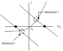
When the applied AC voltage starts decreasing and less than the capacitor, the capacitor starts decreasing slowly which is slower when compared to the charging of the capacitor and it does not get enough time to discharge entirely and the charging starts again.
So around half of the charge present in the capacitor gets discharged. During the negative cycle, D2 starts conducting, and the above process repeats . This will cause the current to flow through the same direction across the load.
Characteristics:
Ripple Factor (γ)
γ=  /Vdc) 2 – 1
The output of the rectifier consists of both AC and DC components. The AC components are undesirable to us and will cause pulsations in the output. This unwanted AC components are called Ripple. The expression ripple factor is given above where Vrms is the RMS value of the AC component and Vdc is the DC component in the rectifier.
For centre-tapped full-wave rectifier, we obtain γ = 0.48
Rectifier Efficiency (η)
Rectifier efficiency is the ratio between the output DC power and the input AC power.
ղ = Pdc / Pac
For centre-tapped full-wave rectifier, ηmax = 81.2%
Form Factor (F.F)
The form factor is the ratio between RMS value and average value.
FF = RMS value / Average value
For centre-tapped full wave rectifier, FF = 1.11
Advantages of Full Wave Rectifiers
- Full wave rectifiers have higher rectifying efficiency than half wave rectifiers . This means that they convert AC to DC more efficiently.
- They have low power loss because no voltage signal is wasted in the rectification process.
- The output voltage of centre-tapped full wave rectifier has lower ripples than a halfwave rectifiers.
Disadvantages of Full Wave Rectifiers
- The centre-tapped rectifier is more expensive than half-wave rectifier and tends to occupy a lot of space.
The satisfactory explanation of this breakdown of the junction was first given by the American scientist C. Zener. A Zener diode is a special type of diode that is designed to operate in the reverse breakdown region.
An ordinary diode operated in this region will usually be destroyed due to excessive current. This is not the case for the Zener diode.
It has already been discussed that when the reverse bias on a crystal diode is increased, a critical voltage, called breakdown voltage is reached where the reverse current increases sharply to a high value. The breakdown region is the knee of the reverse characteristic as shown in Figure 32.
The breakdown voltage is sometimes called Zener voltage and the sudden increase in current is known as Zener current.
The breakdown or Zener voltage depends upon the amount of doping. If the diode is heavily doped, depletion layer will be thin and consequently the breakdown of the junction will occur at a lower reverse voltage.
On the other hand, a lightly doped diode has a higher breakdown voltage. When an ordinary crystal diode is properly doped so that it has a sharp breakdown voltage, it is called a Zener diode. A properly doped crystal diode which has a sharp breakdown voltage is known as a Zener diode.
Figure shows the symbol of a Zener diode. It may be seen that it is just like an ordinal, diode except that the bar is turned into z-shape.
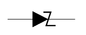
Figure 5: Symbol of a Zener diode
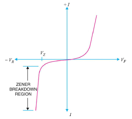
Figure 6: I-V characteristics of Zener diode
As the curve reveals, two things happen when Vz is reached:
- The diode current increases rapidly.
- The reverse voltage Vz across the diode remains almost constant.
The following points may be noted
(i) A Zener diode is like an ordinary diode except that it is properly doped so as to have a sharp breakdown voltage.
(ii) A Zener diode is always reverse connected i.e. it is always reverse biased.
(iii) A Zener diode has sharp breakdown voltage, called Zener voltage Vz.
(iv) When forward biased, its characteristics are just those of ordinary PN junction diode.
(v) The Zener diode is not immediately burnt just because it has entered the breakdown region. As long as the external circuit connected to the diode limits the diode current to less than burn out value, the diode will not burn out.
In other words, the Zener diode operated in this region will have a relatively constant voltage across it, regardless of the value of current through the device. This permits the Zener diode to be used as a voltage regulator or voltage stabiliser.
Key Takeaways
- A Zener diode is a special type of diode that is designed to operate in the reverse breakdown region.
- The breakdown region is the knee of the reverse characteristic
- The breakdown voltage is sometimes called Zener voltage and the sudden increase in current is known as Zener current.
- The breakdown or Zener voltage depends upon the amount of doping.
- Because of its special characteristics Zener diode used as voltage stabiliser
Applications of Zener diode
The basic applications of Zener diode are in overvoltage protection and as a voltage regulator.
Overvoltage Protection
As in Zener diode in reverse bias the current flowing through the diode is more than the normal value. In normal circuits current should not exceed a certain value but due to some problems or fault in the system the current exceeds the maximum range, which can damage the device. To reduce change in voltage at the output due to this current an SCR is connected which cuts down the voltage and disconnects the input source power. The circuit is as shown
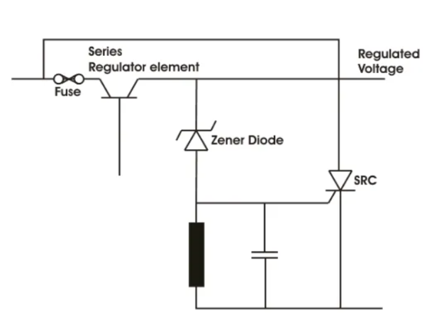
Fig 7. Overvoltage protection Circuit
As Voltage Regulator
This diode can be used to control the voltage in any circuit. There is constant output voltage at the output and it is driven by a current source. When voltage across the diode is more than certain value than excess current is drawn from the supply. To limit current a resistor is used whose value is calculated as
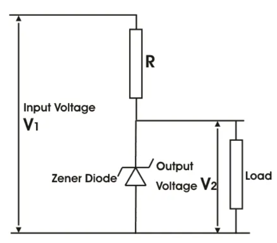
Fig 8. Zener Diode as Voltage Regulator
Resistor value = [(V1-V2)/ (Zener current + load current)]
As the regulating element connected in circuit is in parallel hence it is called as shunt regulator. The Zener diode produce a stable reference voltage across the load which fulfils the criterion of the regulator.
The photodiode is a p-n junction semiconductor diode which is always operated in the reverse biased condition.
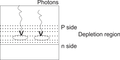
The light is always focused through a glass lens on the junction of the photodiode As the photodiode is reverse biased the depletion region is quite wide, penetrated on both side of the junction.
The photons incident on the depletion region will impact their energy to the Ions present in depletion region and generates e hole pairs.
The photons incident on the depletion region so the number of electron hole pairs will be generated depends on the intensity of light [number of photons] These and holes will be attracted towards the +ve& -ve terminals respectively of the photo current,
With increase in the light intensity a greater number of e hole pairs are generated and the photo current increases thus the photocurrent is proportional to the light intensity.
LED or Light emitting diode
Light emitting diode is a pn junction device. It is always operated in forward biased condition. LED converts electrical energy into light energy.
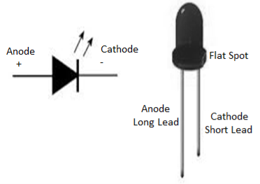
Figure 9: LED
Device Structure:
The LED structure plays a crucial role in emitting light from the LED surface. The LEDs are structured to ensure most of the recombination takes place on the surface by the following two ways.
- By increasing the doping concentration of the substrate, so that additional free minority charge carrier’s electrons move to the top, recombine and emit light at the surface.
- By increasing the diffusion length L =√Dτ, where D is the diffusion coefficient and τ is the carrier life time.
But when increased beyond a critical length there is a chance of reabsorption of the photons into the device. The LED has to be structured so that the photons generated from the device are emitted without being reabsorbed.
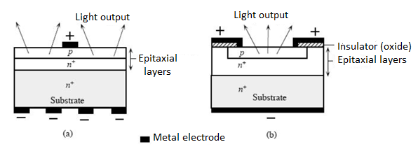
Figure 10: A schematic illustration of typical planar surface emitting LED devices. (a) p-layer grown epitaxially on an n+ substrate. (b) First n+ is epitaxially grown and then p region is formed by dopant diffusion into the epitaxial layer.
One solution is to make the p layer on the top thin, enough to create a depletion layer. Following picture shows the layered structure. There are different ways to structure the dome for efficient emitting
LEDs are usually built on an n-type substrate, with an electrode attached to the p-type layer deposited on its surface. P-type substrates, while less common, occur as well. Many commercial LEDs, especially GaN/InGaN, also use sapphire substrate.
In the fabrication of LED’s direct band gap semiconductors like GaP, GaAsP are used. In direct band gap semiconductor most of the energy is emitted in the form of light when hole and electron recombination takes place.
When an LED is forward biased the electrons and holes move in towards the junction and recombination takes place. As a result of recombination the electrons lying in the conduction band of an n- region fall into the holes lying in the valence band of a p –region. The difference of energy in the valence band and conduction band is radiated in the form of light energy. Here their excess energy is transferred to the emitted photon. The brightness of emitted light is directly proportional to the forward bias current.
Figures of Merit
A very important metric of an LED is the external quantum efficiency ηext. It quantifies the efficiency of the conversion of electrical energy into emitted optical energy.
Not all the photons emitted from the active region of an LED make it out of the device. Some are reabsorbed, some go in the wrong direction, some are reflected back. The light extraction efficiency of a LED is,
ηextraction 
The external quantum efficiency ext of a LED is,
ηextraction 
It is defined as the light output divided by the electrical input power. It is also defined as the product of Internal radiative efficiency and Extraction efficiency. ηext = Pout(optical)/ IV
For indirect bandgap semiconductors ηext is generally less than 1%, whereas for a direct band gap material it could be substantial.
ηint = rate of radiation recombination/ Total recombination
The internal efficiency is a function of the quality of the material and the structure and composition of the layer.
LED materials
LEDs are comprised of compound semiconductor materials, which are made up of elements from group III and group V of the periodic table (these are known as III-V materials). Examples of III-V materials commonly used to make LEDs are gallium arsenide (GaAs) and gallium phosphide (GaP).
Ternary alloys based on alloying GaAs and GaP which are denoted by GaAs1-yPy. Inga Alp is an example of a quaternary (four elements) III-V alloy with a direct band gap. The LEDs realized using two differently doped semiconductors that are the same material is called a homojunction. When they are realized using different bandgap materials they are called a heterostructure device. A heterostructure LED is brighter than a homoJunction LED.
The main semiconductor materials used to manufacture LEDs are:
- Indium gallium nitride (InGaN): blue, green and ultraviolet high-brightness LEDs
- Aluminium gallium indium phosphide (AlGaInP): yellow, orange and red high-brightness LEDs
- Aluminium gallium arsenide (AlGaAs): red and infrared LEDs
- Gallium phosphide (GaP): yellow and green LEDs
Characteristics of LED
LEDs are solid-state devices. The advantages are:
1) Light Generated by LED is Directional
2) LED can Generate Different Light Colour
3) Temperature will Affect LED Efficacy
4) Low Energy Consumption
5) Long Life
The usage of LED is advantageous as it consumes less power and produces less heat. LEDs last longer than incandescent lamps.
Applications LEDs are used in
- For instrument display
- In calculators
- Digital clocks
- For indicating power ON/ OFF
- For optical switching application
- In optical communication system
- Medical devices
Key Takeaways
- Light emitting diode is a pn junction device. It is always operated in forward biased condition. LED converts electrical energy into light energy.
- When an LED is forward biased the electrons and holes move in towards the junction and recombination takes place.
- The light extraction efficiency of a LED is,
ηextraction 
- LEDs are comprised of compound semiconductor materials, which are made up of elements from group III and group V of the periodic table (these are known as III-V materials). Examples of III-V materials commonly used to make LEDs are gallium arsenide (GaAs) and gallium phosphide (GaP).
A scientist named Walter. H. Schottky first discovered Schottky diode. A Shockley diode is a PNPN device having two terminals. This device consists of four alternate P-type and N-type layers in a single crystal and acts as a switch. The various layers are labelled as P1, N1, P2, and N2 for identification.
Since a P-region adjacent to an N-region may be considered a junction diode, the Shockley diode is equivalent to three junction diodes connected in series as shown in Figure (ii). The symbol of Shockley diode is shown in Figure (iii).
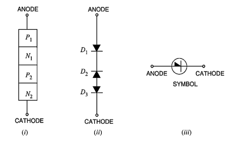
Figure 11: (i) Shockley diode (ii) equivalent figure to Shockley diode (iii)The symbol of Shockley diode
Schottky diode is a device, which comes under the type of a metal semiconductor junction diode. Barrier diode and low voltage diodes are the other names for Schottky diode. When compared to a PN junction diode, power drop is lower in Schottky diode.
Working
When we forward biased the Shockley diode i.e., making anode is more positive w.r.t. Cathode, as a result diodes D1 and D3 would be forward-biased while diode D2 would be reverse-biased. Since diode D2 offers very high resistance and the three diodes are in series, the Shockley diode presents a very high resistance. As the forward voltage increases, the reverse bias across D2 is also increased.
If we keep on increasing forward biasing a point reached when voltage become break over voltage VBO, reverse breakdown of D2 occurs. Since this breakdown results in reduced resistance, the Shockley diode presents a very low resistance. From now onwards, the Shockley diode behaves as a conventional forward-biased diode; the forward current being determined by the applied voltage and external load resistance.
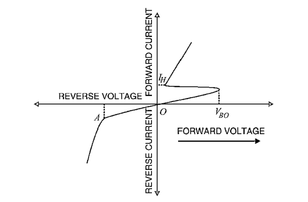
Figure 12: V-I characteristic
When Shockley diode is reverse biased (i.e., anode is negative w. Rt. Cathode), diodes D1 and D3 would be reverse-biased while diode D2 would be forward-biased. If reverse voltage is increased sufficiently, the reverse voltage breakdown (point A in Figure 36) of Shockley diode is reached. At this point, diodes D1 and D3 would go into reverse-voltage breakdown, the reverse current flowing through them would rise rapidly and the heat produced by this current flow could ruin the entire device. For this reason, Shockley diode should never be operated with a reverse voltage sufficient to reach the reverse-voltage breakdown point.
Shockley diode behaves like a switch. So long as the forward voltage is less than break over voltage, Shockley diode offers very high resistance (i.e. switch is open) and practically conducts no current. At voltages above the break-over value, Shockley diode presents a very low resistance (i.e. switch is closed) and Shockley diode conducts heavily.
It may be noted that Shockley diode is also known as PNPN diode or four layer diode or reverse-blocking diode thyristor.
Once Shockley diode is turned ON (i.e., it starts conducting), the only way to turn it OFF is to reduce the applied voltage to such a value so that current flowing through Shockley diode drops below its holding current IH value. Diode D2 then comes out of its reverse-breakdown state and its high-resistance value is restored. This, in turn, causes the entire Shockley diode to revert to its high-resistance (switch open) state.
Key Takeaways
- A Shockley diode is a PNPN device having two terminals.
- Shockley diode behaves like a switch.
- It may be noted that Shockley diode is also known as PNPN diode or four-layer diode or reverse-blocking diode thyristor.
- Once Shockley diode is turned ON (i.e., it starts conducting), the only way to turn it OFF is to reduce the applied voltage to such a value so that current flowing through Shockley diode drops below its holding current IH value.
By utilizing an op-amp and few other external components, linear voltage regulator is built. The same circuit is also a voltage stabilizer, able to stabilize voltage at a grade better than The transistor is used to supply the load with much more current than the op-amp itself could possibly supply.
The D1 diode is a Zener -type diode and it is used for voltage reference.
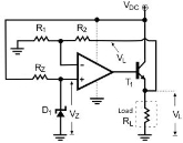
Fig 13. Basic op-amp voltage regulator
D1 is biased through Rz. When correctly reserve biased, the Zener diode keeps the voltage across its leads close to the Zener breakdown voltage. The op-amp is used as a linear voltage amplifier.
Due to the high open loop voltage gain of the op-amp the op-amp remains in its linear region, the voltage difference between its inverting (V-) and non-inverting input (V+) is almost equal to zero.
In other words, the voltage at its non-inverting input, in respect to the ground, equals the voltage at its inverting input:
V-=V+ -------(1)
Equation (1) holds true for any op-amp working at its linear region (as an amplifier).
R1 and R2 form a voltage divider, and the voltage (V-) at their connection point is also given by the well- known voltage-divider formula:
V-=VL·R1/(R1+R2) ------ (2)
However, V+ is also equal to the Zener breakdown voltage (Vz), because the non-inverting input of the op-amp is directly connected to the cathode of the Zener diode.
V+=VZ -----------------(3)
After solving (1),(2) and (3), we get:
VL=VZ·(1+R2/R1) --------------(4)
From equation (4), we conclude that VL voltage which is the voltage applied to the load is directly proportional to the Zener voltage.
As long as Zener voltage remains stable, VL also remains stable. Additionally, the voltage applied to the load, can be easily adjusted by adjusting R1, R2 or both. For continues voltage adjustment, R1 and R2 can be replaced by a potentiometer, having its wiper at the non-inverting input of the op-amp, and its other leads at the ground and the VL line, respectively.
References:
1. J. Millman and A. Grabel, “Microelectronics”, McGraw Hill Education, 1988.
2. P. Horowitz and W. Hill, “The Art of Electronics”, Cambridge University Press, 1989.
3. P. R. Gray, R. G. Meyer and S. Lewis, “Analysis and Design of Analog Integrated Circuits”, John Wiley & Sons, 2001.