Unit - 3
Power amplifiers
The position of the Q-point and the extent of the characteristics that is being used, decides the class of operation of power amplifiers.
The various classes of power amplifiers are –
(i) Class A power amplifier
(ii) Class B power amplifier
(iii) Class C power amplifier
(iv) Class AB power amplifier
1). The intersection of the output characteristics curve and the load line is known as operating point or Q-point of transistor.
2). On this quiescent operating point, if an a.c. Signal is superimposed by the application of a.c. Sinusoidal voltage at the input, the base current varies sinusoidally about its quiescent value IBQ.
3). Since the transistor is biased to operate in the active region, the output is linearly proportional to the input i.e., IC = βIB
4). Hence the collector current also varies sinusoidally about its quiescent value IBQ.
Class A amplifier: A class-A amplifier is the amplifier in which the Q-point of the input signal are selected such that the output signal is obtained for a full input cycle. For this purpose, the position of the Q-point is approximately at the midpoint of the load line.
For all the values of the input signal, the transistor remains in the active region and never enters into cut-off or saturation region.
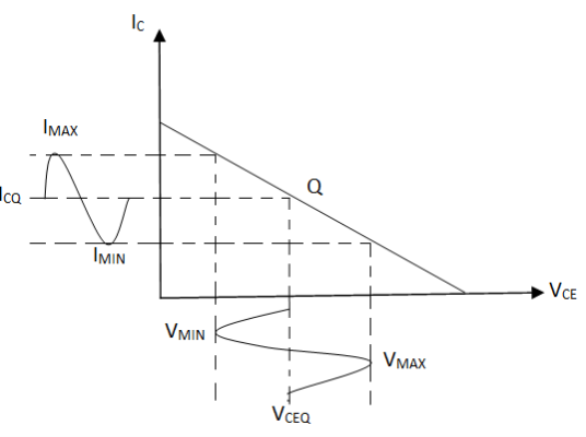
Fig 1. Output characteristics of CE Amplifier
The collector current IC flow for complete 3600 (full cycle) of the input cycles. Thus, the angle of the collector current flow is 3600.
Class A amplifier are of 2 types –
(i) Directly coupled class A amplifier – In directly coupled type, the load is directly connected in the collector circuit.
(ii) Transformer coupled class A amplifier – In this the load is coupled to the collector using a transformer called an output transformer.
(i) Directly coupled class A amplifier –
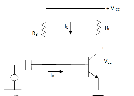
Fig 2. Directly coupled class A amplifier
The value of RB is selected such that Q point lies at the centre of d.c. Load line.
VCC = ICRL + VCE
IBQ = VCC – 0.7 / RB
ICQ = βIBQ
VCEQ = VCC - ICQRL
DC power input: PDC = VCCICQ Watts
The d.c. Power input is provided by the supply:
- With no a.c. Input signal, the d.c. Current drawn is the collector bias current ICQ.
- Even if any a.c. Input signal is applied, the average current drawn from the d.c. Supply remains same.
A.C. Power Output:
Vpp = Vmax - Vmin
Vmin = Min instantaneous value of collector output voltage
Vmax = Max instantaneous value of collector output voltage
Vpp = Peak of a.c. Output voltage
Vm = Vpp / 2 = Vmax – Vmin / 2 = Amplitude of a.c. Output voltage
Im = Ipp / 2 = Imax – Imin / 2
The r.m.s value of alternating output voltage and current is given as
Vrms = Vm / √2 ;Irms = Im / √2
Pac = VrmsIrms = I2rmsRL = V2rms / RL
Pac = Vm /√ 2: Im /√ 2 = 1/2Vmax – Vmin /√ 2. Imax – Imin /√ 2
Pac = ( Vmax - Vmin )( Imax - Imin ) / 8
Efficiency:
% n = Pac / Pdc x 100 %
= [(Vmax - Vmin) (Imax - Imin) / 8 x Vcc x ICQ] x 100%
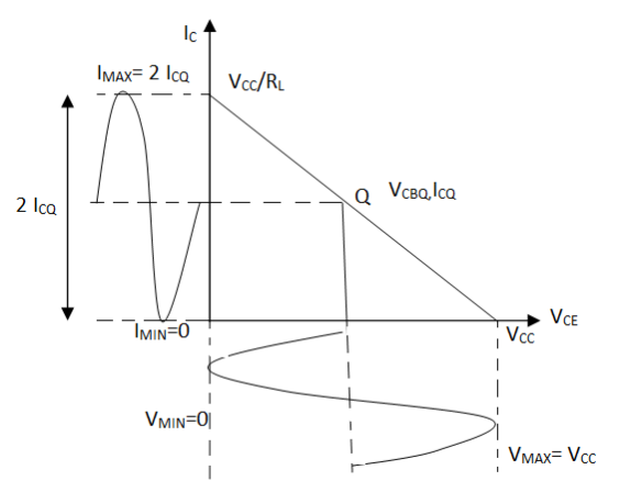
Fig 3. AC Power Output
Maximum Efficiency:
Vmax = Vcc, Vmin = 0
Imax = 2ICQ, Imin = 0 {As Q is in middle}
n = (Vmax - Vmin) (Imax - Imin) / 8 x Vcc. ICQ x 100 %
= (Vcc - 0) (2ICQ - 0) / 8 x Vcc.ICQ x 100 %
Nmax = 25 % {Biggest disadvantage}
Power dissipation ( Pd ): Pd = Pdc - Pac
Power dissipation = D.C. Power input – AC power output
(i) When there is no input signal, then Pac = 0 and the entire d.c power gets dissipated in the form of heat which is maximum PD.
(Pd)max = PDC = VCCICQ when Pac = 0
(ii) When input signal is larger, more power is delivered to load (Pac is more) and less is the power dissipation.
Thus, class A amplifier dissipated less power when delivers maximum power to the load while it dissipates maximum power while delivering zero power to the load.
Disadvantages:
(i) The load resistance is connected directly to collector, hence quiescent current passes through this resistance. This current represents a considerable waste of power, since it doesn’t contribute to the a.c. Component of the power. Also, it is inadvisable to pass the d.c. Component of current through the output device.
(ii) Efficiency is poor.
(ii) Transformer coupled Amplifier:
Generally, the output impedance of the transistor is much higher than the input impedance (RL) of the loudspeaker. Hence most of the power generated would be lost in the transistor.
To transfer a significant amount of power to the load, it is necessary to use an output matching transistor.
Applying KVL: VCC – VCEQ = 0 => VCEQ = VCC
DC power input: PDC = VCCICQ
Where,
RL = load on secondary
R2 = Reflected load on the primary or effective load as seen by primary
RL1 = (N1 / N2 )2 RL
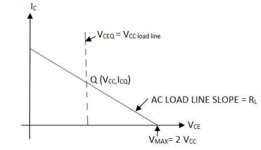
Fig 4. Load Line
AC power output Pac:
Pac = (Vmax - Vmin) (Imax - Imin) / 8
Pac = I12rmsRL1 = I22rmsRL = V1rmsI1rms = V2rmsI2rms
Where V1rms = RMS value of primary voltage
V2rms = RMS value of secondary voltage
Efficiency (n): n = Pac / Pdc x 100 %
Max efficiency:
Vmin = 0, Vmax = 2VCC
Imin = 0, Imax = 2ICQ
% nmax = 50 %
Class B amplifier– In class B amplifiers, the Q point and the input signal is selected, such that the output signal is obtained only for one half cycle for a full input cycle.
Either the quiescent current or the quiescent voltage is approximately zero. If quiescent current is zero, then the transistor is in cut off region, and the transistor remains in active region only for the half cycle of the input signal. Hence at output we get only the half cycle.
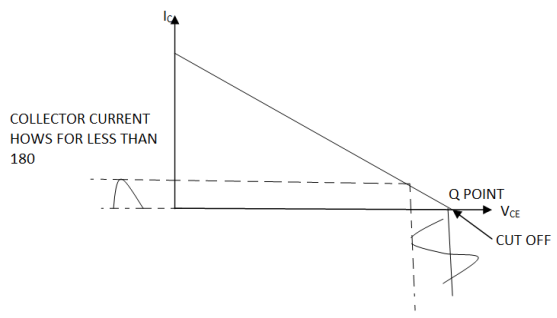
Fig 5. Load line characteristics of class B amplifier
If instead of ICQ = 0, we would have taken VCEQ = 0(i.e., Q point on Y-axis) then the transistor would have been in saturation region and the collector current flows only for negative half cycle of the input signal.
Efficiency of this mode is higher than class A mode.
Since in this mode, collector current flows only for half cycle, so that output signal is distorted. To get the full cycle, a pair of transistors is used in class B operation. The 2 transistors conduct in alternate half cycles of the input signal abd so a full cycle across the load is obtained. The two transistors are identical in characteristics and are called matched transistors.
Depending upon the types of 2 transistors, the two different circuit configurations of Class B are –
(i) Push Pull Class B amplifier
(ii) Complimentary Symmetry Class B
(i) Push Pull Class B amplifier: When both the transistors are of some type i.e., either n-p-n or p-n-p, then the circuit is called push-pull class B audio frequency power amplifier.
The push pull circuit requires 2 transformers, one as input transformer called driver transformer and the other to connect the load called output transformer. The input signal is applied to the primary of the driver transformer. Both the transformer is centre tapped transformers.
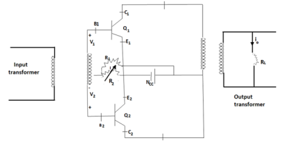
Fig 6.Push pull amplifier
In the circuit, both Q1 and Q2 are of n-p-n type. p-n-p can also be used but with -VCC. Both are in CE configuration.
Operation:
Case (i) – During positive half cycle,
Q1 = ON, Q2 = OFF
IO1α iC1
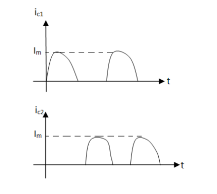
Fig 7. Positive half cycle output
Case (ii) – During negative half cycle,
Q1 = OFF, Q2 = ON
IO2α iC2
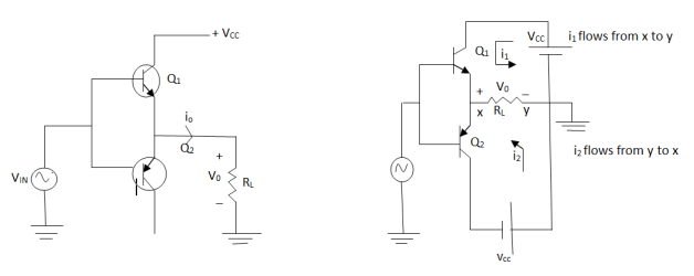
Fig 8. Positive half cycle output
Case (iii) When signal is absent i.e., V1 = V2 = 0
If R2 = 0 then,
VBE1 = VBE2 = 0
Both Q1, Q2 are in cut off [ Class B operation]
Case (iv) If R2 increases then IR2 increases and when IR2 = Vr then
VBE1 = VBE2 = Vr [ Class AB operation]
Case (v) If R2 increases more, then IR2 increases VBE increases and Q point will move towards saturation.
The total d.c. Power is given by,
Pdc = VCC x Idc
= 2 / ∏ VCC Im
a.c. Power, Pac = Vrms.Irms
= I2rmsR1L = V2rms / R1L
Efficiency:
% n = Pac / Pdc x 100 %
= ( Vm.Im / 2 ) / 2 / ∏VCCIm
% n = ∏ / 4 Vm / VCC x 100 %
Max Efficiency:
Max efficiency is possible only if, Vm = VCC
% nmax = ∏ / 4 VCC / Vcc x 100 = 78.5 %
Power dissipation:
Pd = Pdc - Pac
= 2 / ∏ VCCIm - Vm.Im / 2
= 2 / ∏ VCCVm/ R1L - Vm2 / 2 R1L
Maximum power dissipation:
For max power dissipation,
DPd / dVm = 2 / ∏ VCC / R1L - 2Vm/ 2 R1L = 0
2 / ∏ VCC / R1L = Vm/ R1L
Vm = 2 / ∏ VCC
This is the condition for max power dissipation,
Hence max power dissipation is given by,
(Pd)max= 2 / ∏ VCC x 2 / ∏ VCC / R1L - 4 / ∏2 VCC2 / 2R1L
= 4 / ∏2 VCC2 / R1L - 2 / ∏2 VCC2 / R1L
(Pd)max= 2 / ∏2 VCC2 / R1L
For max efficiency Vm = VCC hence the dissipation is not maximum when the efficiency is maximum and when power dissipation is maximum, efficiency is not maximum.
The a.c. Power is given by,
Pac = Vm2 / 2RL1
Where Vm = VCC is the maximum condition.
The maximum a.c. Power is given by
(Pac)max = VCC2 / 2RL1
(Pd)max = 2VCC2 / ∏2RL1 = 4 / ∏2( VCC2 / 2RL1 )
(Pd)max = 4 / ∏2 (Pac)max
The maximum power dissipation per transistor is given by,
(Pd)max per transistor = 4 / ∏2 (Pac)max / 2
= 2 / ∏2 (Pac)max
Advantages:
- Efficiency is much higher than the class A operation.
- When there is no input signal, the power dissipation is zero.
- Ripples present in supply voltage also get eliminated.
- Due to transformers, impedance matching is possible.
Disadvantages:
- 2 centre tap transformers are necessary
- Transformers make the circuit bulky and costlier.
- Frequency response is poor.
Complementary Symmetry Class B push pull amplifier –
This circuit is transformer less circuit. But with common emitter configuration, it becomes difficult to match the output impedance for maximum power transfer with output transformer. Hence the matched pair of complementary transistors is used in common collector (emitter follower) configuration in this circuit.
This is because common collector configuration has lowest output impedance and hence the impedance matching is possible.
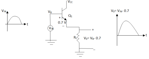
Fig 9. Complimentary symmetry Push pull amplifier
The circuit is driven from a dual supply of +-VCC. The transistor Q1 is n-p-n while Q2 is p-n-p type.
Operation:
During positive half cycle:

Fig 10. Positive half cycle operation
During negative half cycle:
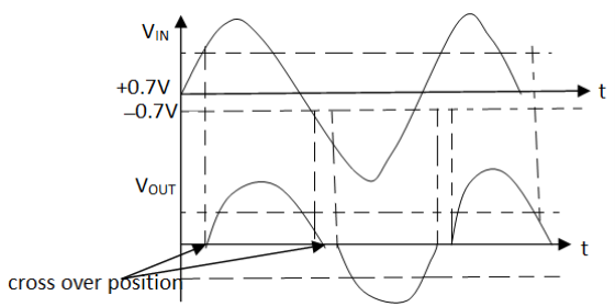
Fig 11. Negative half cycle operation
Cross over distortion:
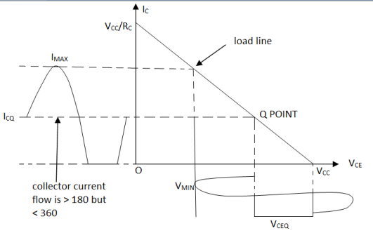
Fig 12. Crossover Distortion
Advantages:
(i) As the circuit is transformer less, its weight, size and cost are less.
(ii) Due to common collector configuration, impedance matching is possible.
(iii) The frequency response improves due to transformer less class B amplifier circuit.
Disadvantages:
(i) The circuit needs two separate voltage supplies.
(ii) The output is distorted to cross-over distortion.
Class AB amplifiers (between A and B):
In class AB amplifiers, the Q-point and the input signal are selected such that the output signal is obtained for more than a half cycle but less than a full cycle.

Fig 13. Characteristic curve for class AB operation
The Q point is below the midpoint but above X-axis or above the midpoint but to the right of Y-axis. Its efficiency is more than class A but less than class B. Efficiency increases as the Q-point moves away from the centre of the load line.
Numerical:
Q-1 – Determine the input power, output power and efficiency resulting in a class B push-pull amplifier providing a signal 20V peak to a 16 Ω load, using a single supply of VCC = 30V.
Sol. Given: VL(p) = 20 V, RL = 16 Ω, VCC = 30 V
The input power is given by,
Pi(dc) = VCC(2 / ∏ I / p) = VCC.2 / ∏.VL(p) / RL
= 30 x 2 / ∏ x 20 / 16 = 23.87 W Ans.
The output power is given by,
PO(ac) = VL2(p) / 2RL = VL2(rms) / 2RL = (20)2 / 2 x 16 = 12.5 W Ans.
Thus, efficiency is given by,
n = PO(ac) / Pi(dc) x 100 = 12.5 / 23.87 x 100 = 52.37 % Ans.
Q-2 – Class B complementary A.F. Power amplifier shown in the below figure
Calculate:
- Maximum a.c. Power which can be developed.
- Collector dissipation while developing maximum a.c. Power.
- Efficiency
- Maximum power dissipation per transistor.
- Efficiency under maximum power dissipation condition Assume sinusoidal input.
Soln. Given: VC = 15 V, RL = 4 Ω
Use the expression derived for push pull class B.
- The maximum a.c. Power is,
(Pac)max = 1/2VCC2 / RL = 1/2(15)2 / 4 = 28.125 W Ans
- When power developed is maximum, Vm = VCC
RL = Vm / Im
Im= Vm / RL = VCC / RL = 15 / 4 = 3.75 A
Pdc = 2 / ∏VCCIm = 2 / ∏ x 1.5 x 3.75 = 35.809 W
Pd = Pdc – Pac = 35.809 – 28.125 = 7.684 W Ans.
This is the total collector dissipation under maximum power conditions.
- Efficiency:
% n = Pac / Pdc x 100 = 28.125 / 38.809 x 100 = 78.5 % Ans.
The efficiency is maximum possible for class B, due to the fact that the power developed is at its maximum.
- For maximum power dissipation,
Vm = 2 / ∏ VCC = 2 / ∏ x 15 = 9.5492 V
Im = Vm / RL = 9.5492 / 4 = 2.3873 A
Pdc = 2 / ∏ VCC Im = 2 / ∏ x 15 x 2.3873 = 22.797 W
While Pac = 1/2Vm2 / RL = 1/2(9.5492)2 / 4 = 11.398 W
(Pd)max = Pdc – Pac = 22.797 – 11.398 = 11.39 W
(Pd)max = 11.39 / 2 = 5.699 W [ Per transistor]
Alternatively, we can directly use the result,
(Pd)max = 2 / ∏2 (Pac)max per transistor
= 2 / ∏2 x 28.125 = 5.699 W per transistor Ans.
- Efficiency under (Pd)max condition,
% n = Pac under (Pd)max / Pdc under (Pd)max x 100
= 11.398 / 22.797 x 100 = 50 % Ans.
This shows that when efficiency is maximum, power dissipation is not maximum and when power dissipation is maximum, efficiency is not maximum.
Q-3 – (A) A series fed class A amplifier uses a supply voltage of 10 V and load resistance of 20 Ω. The a.c. Input voltage results in a base current of 4 mA peak. Calculate,
- D.C. Input power
- A.C. Output power
- % Efficiency
Assume β of the transistor as 25 and the collector bias current of 50 mA.
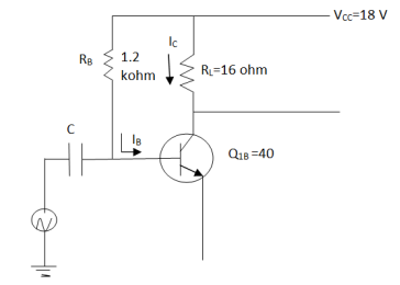
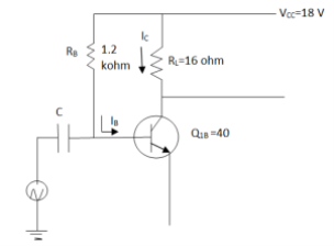
(B) Calculate the input power, output power & the efficiency of class A amplifier shown in figure. The input voltage causes a base current 5mA rms.
Sol :(A) Given: VCC = 10 V, (ib)m = 4 mA, β = 25, ICQ = 50 mA, RL = 20 Ω
- D.C. Input power:
PDC = VCCICQ = 10 x 50 x 10-3 = 0.5 W Ans.
- A.C. Output power:
(ic)m = β(ib)m = 25 x 4 = 100 mA
But ic is the output current I.
Im = 100 mA
Pac = I2mRL / 2 = (100 x 10-3)2 x 20 / 2 = 0.1 W Ans.
- % Efficiency:
% n = Pac / Pdc x 100 = 0.1 / 0.5 x 100 = 20 % Ans
(B) Given class A amplifier is shown in below figure

Current IBQ can be written as,
IBQ = VCC – 0.7 / RB = 18 – 0.7 / 1.2 x 103 = 14.4167 mA
Now, ICQ = βIBQ = 40 x 14.4167 = 576.67 mA
And, VCEQ = VCC – ICQ RL = 18 – 576.67 x 10-7 x 16 = 8.7733 V
So, Pdc = VCCICQ = 18 x 576.67 = 10.38 W Ans.
This is the input power.
(Ib)rms = 5 mA
(Ic)rms = β(Ib)rms = 40 x 5 = 200 mA
This is nothing but the output collector current r.m.s value Irms.
Irms = 200 mA
Output power can be written as,
Pac = I2rms RL = (200 x 10-3) x 16 = 640 mW
This is the power delivered to the load.
Hence the efficiency of the amplifier is,
% n = Pac / Pdc x 100 = 640 x 10-3 / 10.38 x 100
% n = 6.165 % Ans.
Q-4 - For a class B amplifier using common collector configuration, the supply voltage is 25 V while the load resistance is 16 Ω. If the input a.c. Signal of 20 V peak is supplied, determine the input power, output power and the efficiency.
Sol. Given: VCC = 25 V, Vm = 20 V, RL = 16 Ω
For a common collector configuration, the voltage is 1.
Vin(peak) = Vout(peak) = 20 V
Now, Vm / Im = RL
Im = Vm / RL = 20 / 16 = 1.25 A
The input power is given by,
PDC = 2 / ∏ = VCCIm = 2 / ∏ x 25 x 1.25 = 19.8943 W Ans.
The output power is given by,
Pac = Vm Im / 2 = 20 x 1.25 / 2 = 12.5 W Ans.
Thus, efficiency is given by,
% n = Pac / Pdc x 100 = 12.5 / 19.8943 x 100 = 62.832 % Ans.
The application of a sinusoidal signal to the input of an ideal amplifier will result in a sinusoidal output wave. Generally, the output wave is not an exact replica of the input signal waveform because of various types of errors. The types of distortion that may exist are –
(i) Non-linear distortion –We have assumed that the dynamic transfer wave for the transistor is linear i.e. IC = βIB. But the transfer curve is nonlinear of the form,
IC = K1IB + K2IB2 + K3IB3 + - - -
Due to this, the new frequencies at the output is produced which are not present in the input. This type of distortion is sometime referred as ‘amplitude distortion’.
(ii) Frequency distortion –This type of distortion exist when the signal components of different frequencies are amplified differently.
(iii) Phase-Shift distortion -It results from the unequal phase shifts of the signals of different frequencies.
Feedback Amplifier is a device that is based on the principle of feedback. The process by which some part or fraction of output is combined with the input is known as feedback.
Feedback amplifiers are the type of amplifiers in which a part of the output is given back to the input.
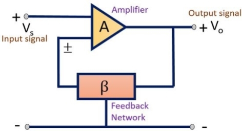
Amplifier is a device that amplifies the signal. In an ideal amplifier, there exist some important characteristics like voltage gain, input impedance, output impedance, bandwidth etc.
These parameters of an amplifier are controlled by employing a feedback network. Thus, a feedback network is employed in an amplifier to control the gain and other factors of the device.
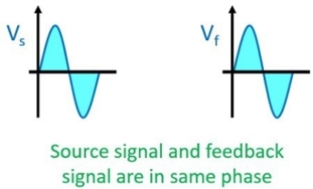
Positive Feedback amplifier– It is a type of an amplifier in which source signal and the feedback signal are in the same phase. Thus, the feedback signal applied increases the strength of the input signal.
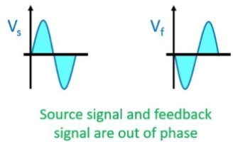
Negative Feedback amplifier– In this type of amplifier source signal and the feedback signal are out of phase with each other. Thus, the feedback signal applied to decrease the strength of the input signal.

An input signal Vs is applied to the amplifier with gain A, that produces an amplified signal, Vo.
A portion or fraction of this Vo is then fed to a feedback network having gain β. The output of feedback network is Vf, this signal is then given to summer or a mixer that resultantly produces either sum or difference of two signal depending on their phase relationship.
The gain of an amplifier is given as the ratio of output voltage or current to the input voltage or current.
The gain of the circuit without feedback is given as
A= Vo/Vd -----------------(1)
The gain of feedback network is given as
β = Vf/Vo ----------------(2)
Vd is the mixer output voltage given by
Vd = Vs ± Vf --------------------------(3)
The signal voltage Vs and mixer output voltage Vd will only be equal in a feedback amplifier unless the output is not generated.
From Eq 1 we can write as
Vo = A Vd -----------------------------------(4)
Substituting the value Vd in eq 4
Vo = A[ Vs ± Vf] -------------------------------(5)
From Eq 2
Vf = β Vo ------------------------------------(6)
Substituting the value of Vf in eq 5
Vo = A[ Vs ± β Vo]
Vo = A Vs ± A β Vo
Vo ± A β Vo = A Vs
Vo[1± Aβ] = A Vs
Vo/Vs = A / 1 ± Aβ
Avf = A/ 1 ± Aβ where Vo/Vs = Avf
This is the desired value for the gain of the feedback amplifier.
The gain of an amplifier is always greater than 1. This simply means that some elements are present which increases the gain of the amplifier. That element can be a transistor or a MOSFET.
But a feedback network is always a linear network consisting of RLC elements and it does not contain any such amplification device.
That’s why the value of Vf is always less than Vo.
So,β < 1
In case of a positive feedback the source signal will be in phase with that of the feedback signal.
Thus, the mixer will produce the summation of the two signal applied to it in case of positive feedback.
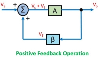
So, the gain of the amplifier is given as
Avf = A/ 1 - Aβ
This is the gain for a positive feedback amplifier.
The source signal and the feedback signal are out of phase with respect to each other.
Thus, the mixer circuit will resultantly produce the difference between the two signal in case of a negative feedback amplifier.
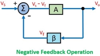
So, in this case, the gain of the amplifier is given as
Avf = A / 1+Aβ
For a negative feedback, the value of denominator is always greater than 1, this will decrease the overall gain of the system by the factor 1 +Aβ.
In case of a positive feedback system, the value of denominator is always less than 1, this will resultantly increase the overall gain by 1 – Aβ.
Gain Stability Relation
For an ideal system, the gain of the amplifier is infinite. Thus, for a smaller input, we will have a much higher value as output. So, such a large gain is not desirable in the circuit.
The system becomes stable only when its gain is small.
Hence, by decreasing the gain the stability of the system increases and vice-versa.
So, to have a stable system, the gain of the amplifier must be small and it is achieved by employing negative feedback in the circuit.
Barkhausen Condition – Condition that are required to be satisfied to operate the circuit as an oscillator are called as Barkhausen condition.
In oscillator circuit there is no input signal hence the feedback signal it say should be sufficient to maintain the oscillations.
Barkhausen condition states that
- The loop gain (Aβ) is equal to unity i.e.

- The phase shift around the loop is zero or an inteqer multiple of 2
i.e. π<βA = 2n
Where n=0,1,2,……..
Types of Oscillator- An oscillator circuit is usually made up of transistor. A transistor can work as an oscillator to produce undamped continuous oscillations of any desired frequency it oscillatory and feedback circuits are properly connected to it. The oscillators differ only in the way of feedback to supply losses to the oscillatory circuit. The following are the important oscillators-
- Wein bridge Oscillator
- RC phase shift oscillator
- Hartley Oscillator
- Capitals Oscillator
RC Oscillators
Analysis and Design of RC Phase Shift using BJT
RC phase shift oscillator circuit using BJT is built by cascading 3-RC phase shift networks where each provides 600 phase shift.
RC is known as the collector resistor which stops the transistor’s collector current.
The resistor near the transistors like R & R1 form the voltage divider circuit and RE develops the strength.
The two capacitors Co & CE, where Co is the o/p DC decoupling capacitor & CE is the emitter bypass capacitor correspondingly.
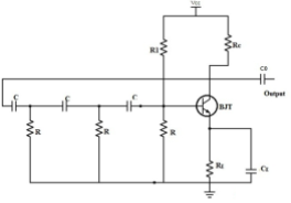
Figure 14. Phase Shift Oscillator using BJT
The circuit causes the o/p waveform to move with 180o throughout from the output terminal toward the transistor’s base terminal. Then this signal is moved again with 180o with the help of transistor within the network because of the truth that the phase disparity among the input as well as the output is 180o in the common emitter (CE) configuration. This creates phase disparity to 360 degrees and satisfies the phase disparity condition.
Frequency of RC Phase Shift Oscillator
The frequency of RC phase shift oscillator is expressed as
f= 1/2πRC√2N
Where,
R is the Resistance (Ohms)
C is the Capacitance
N is the no. Of RC network
The above frequency formula is used for High Pass Filter related design, and also be used LPF.
Design:
For the given data for BC107 hfe=β=110, Ic max=100mA, Vce max = 45V . Let Vcc =12V, Ic=2mA. Since the quiescent point is in the middle of the load line for the amplifier VCE = 50% of Vcc=6V. VRE= 10% of Vcc =1.2 V.
Assume Ic=Ie
VRE = Ic RE = IE RE
1.2 = 2 x 10 -3 x RE
RE = 1.2 / 2 x 10 -3 = 600Ω
The standard value of resistance 560Ω.
Voltage across collector resistance
V RC = Vcc – VCE – VRE
= 12-6-1.2 = 4.8V
Rc = VRC/Ic = 4.8 / 2 x 10 -3 = 2.4 kΩ
Select 2.2 kΩ
Base current IB = Ic/ β = 2 x 10 -3 / 110 = 18.2 μA
Take I2 = IB then I1 = 10IB + IB = 11 IB
Base Voltage VB = VRE + VBE = 1.2 + 0.6 = 1.8 V
R2 = VB/I2 = 1.8 / 10 x 18.2 x 10 -6 = 9.9kΩ
Select R2= 10kΩ
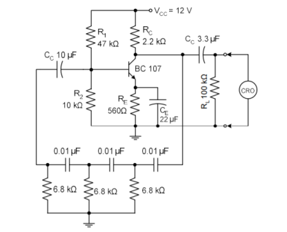
Figure 15. Circuit Diagram of RC Phase Shift Oscillator
R1 = Vcc – VB/ I1 = 12-1.8 / 11 x 18.2 x 10 -6 = 51 kΩ
Design of coupling capacitors CC1 and CC2
XC1 should be less than the input impedance of the transistor. Here, Rin is the series impedance.
Then Xc1 ≤ Rin/10
Here Rin= R1||R2||hfe rE = 47 kΩ||10kΩ||10 x 12.5 Ω = 1.17kΩ
We get Rin = 1.17kΩ Then Xc ≤117Ω.
For a lower cut off frequency of 200Hz CC1 = 1/ 2π f Xc1 = 1/2π x 200 x 117 = 6.8 μF
Select standard value of 10 μF for CC1
Similarly Xc2≤Rout/10 where Rout = RC . Then XCE ≤220Ω
So CC2 = 1/ 2 π f XC2 = 1/ 2π x 200 x 220 = 3.6 μF
Select standard value of 3.3 μF for CC2.
Design of bypass capacitors CE
To bypass the lowest frequency XCE should be much less than or equal to the resistance RE.
XCE ≤ RE/10.
XCE ≤ 560/10 that is XCE ≤56.
CE ≥1/ 2 π f XCE = 1/ 2π x 200 x 56 = 14.2 μF.
Select standard value of 22 μF for CE.
Design of feedback network
The circuit consists of an amplifier stage and a feedback network to provide an additional 180⁰ phase shift, approximately depending upon the frequency of operation. The RC phase shift network must provide 180⁰ or an average of 60⁰ phase shift/lag of RC network.
RC phase shift factor k=Vs/Vo
For one stage of RC network
Vo = IR VC = I Xc
Tan ɸ = Vc/Vo = IXC / R = 1/ (2πfC) R
= 1/2πRC tan ɸ
If these are three sections each must give approximately ɸ=60 then tan 60 = √3
f = 1/2πRC √3
In the above phase relationship, between voltage and current in the RC network, the additional current I that flow through C for the other sections so that VC is larger than the value indicated which means that f is smaller than the value obtained in the above equation.
A three-stage network would has frequency of oscillation given by
f = 1/2πRC √6
Assume f = 1000 Hz and C = 0.01 μF.
Analysis and Design of RC phase shift using FET
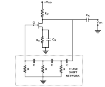
Figure 16. RC Phase Shift Oscillator using FET
The amplifier stage is self- biased with a capacitor bypassed source resistor Rs and a drain bias resistor RD.
The FET device parameters of interest are gm and rd.
- |A| = gmRL, where RL = (RDrd / RD + rd)
- At the operating frequency, the input impedance of the amplifier is infinite.
- This is a valid approximation provided, the oscillator operating frequency is low enough so that FET capacitive impedances can be neglected.
- The output impedance of the amplifier stage given by RL should also be small compared to the impedance seen looking into the feedback network so that no attenuation due to loading occurs.
Design of RC Phase shift using FET
It is desired to design a phase shift oscillator using an FET having gm = 5000µS, rd = 40 kΩ , and a feedback circuit value of R = 10 kΩ. Select the value of C for oscillator operation at 5 kHz and RD for A > 29 to ensure oscillator action.
Solution:
f = 1/2√π6RC ;
C = 1/2√π6Rf = 1.3nF
|A| = gm RL
Let A = 40;
RL = |A| / gm = 8 kΩ
Key Takeaway:
The basic RC Oscillator which is also known as a Phase-shift Oscillator, produces a sine wave output signal using regenerative feedback obtained from the resistor-capacitor (RC) ladder network.
Crystal Oscillator
Crystal Oscillator can be designed by connecting the crystal into the circuit such that it offers low impedance when operated in series-resonant mode and high impedance when operated in anti-resonant or parallel resonant mode as shown below in figure a and b respectively.
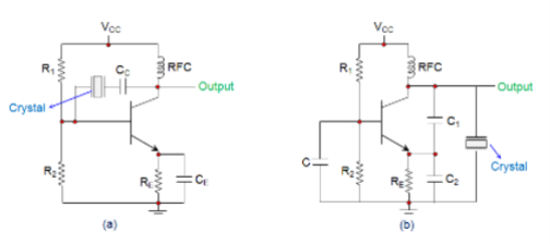
Fig 17(a) Series Resonance Fig 17(b) Parallel Resonance
In the circuits shown, the resistor R1 and R2 form the voltage divider network while the emitter resistor RE stabilizes the circuit. Further, CE (Figure a) acts as an AC bypass capacitor while the coupling capacitor CC (Figure a) is used to block DC signal propagation between the collector and the base terminals. Next, the capacitors C1 and C2 form the capacitive voltage divider network in the case of Figure b.
In addition, there is also a Radio Frequency Coil (RFC) in the circuits (both in Figure a and b) which offers dual advantage as it provides even the DC bias as well as frees the circuit-output from being affected by the AC signal on the power lines.
On supplying the power to the oscillator, the amplitude of the oscillations in the circuit increases until a point is reached wherein the nonlinearities in the amplifier reduce the loop gain to unity. Next, on reaching the steady-state, the crystal in the feedback loop highly influences the frequency of the operating circuit.
Further, here, the frequency will self-adjust so as to facilitate the crystal to present a reactance to the circuit such that the Barkhausen phase requirement is fulfilled.
In general, the frequency of the crystal oscillators will be fixed to be the crystal’s fundamental or characteristic frequency which will be decided by the physical size and shape of the crystal.
However, if the crystal is non-parallel or of non-uniform thickness, then it might resonate at multiple frequencies, resulting in harmonics. Further, the crystal oscillators can be tuned to either even or odd harmonic of the fundamental frequency, which are called Harmonic and Overtone Oscillators, respectively.
Key takeaway
Crystal Oscillator can be designed by connecting the crystal into the circuit such that it offers low impedance when operated in series-resonant mode and high impedance when operated in anti-resonant or parallel resonant mode.
References:
1. J. Millman and A. Grabel, “Microelectronics”, McGraw Hill Education, 1988.
2. P. Horowitz and W. Hill, “The Art of Electronics”, Cambridge University Press, 1989.
3. P. R. Gray, R. G. Meyer and S. Lewis, “Analysis and Design of Analog Integrated
Circuits”, John Wiley & Sons, 2001.