Unit - 1
Fundamentals of Digital Systems and logic families
A digital system understands positional number system where there are few symbols called digits and these symbol represents different values depending on their position in the number.
A value of the digit is determined by using
- The digit
- Its position
- The base of the number system
Binary numbers can represent both positive and negative values, 8 bit systems for example normally use one bit of the byte to represent either + or − and the remaining 7 bits to give the value. One of the simplest of these systems is SIGNED BINARY, also often called ‘Sign and Magnitude’. By convention, a 0 in this position indicates that the number given by the remaining 7 bits is positive, and a most significant bit of 1 indicates that the number is negative.
For example:
+4510 in signed binary is (0)01011012
-4510 in signed binary is (1)01011012
It is an essential part of all the digital calculations.
Binary Addition
- It is a basis for binary subtraction, multiplication, division.
- There are four rules which are as follows:
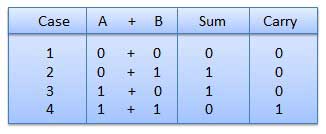
Rules of Binary addition
In fourth step, a sum (1 + 1 = 10) i.e. 0 is written in the given column and a carry of 1 over to the next column is done.
For Example −

Binary addition
Binary Subtraction
Subtraction and Borrow, these are the two words that will be used very frequently for binary subtraction. There rules of binary subtraction are:
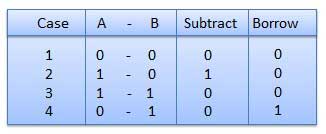
Rules of Binary Subtraction
For Example

Fig. Binary subtraction
Binary Multiplication
- It is similar to decimal multiplication.
- It is also simpler than decimal multiplication as only 0s and 1s are involved.
- There are four rules of binary multiplication which are:
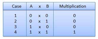
Rules of Binary Multiplication
For Example
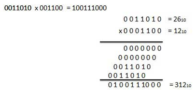
Fig. Binary Multiplication
Binary Division
- It is similar to decimal division.
- It is also called as the long division procedure.
For Example
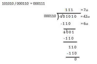
Binary Division
- Complements are used in order to simplify the subtraction operation and the logical manipulations can be done.
- For each radix-r system there are two types of complements:
S.N. | Complement | Description |
1 | Radix Complement | It is referred to as the r's complement. |
2 | Diminished Radix Complement | It is referred to as the (r-1)'s complement. |
- The binary system has radix r = 2.
- Therefore, the two types of complements for the binary system are known as 1's complement and 2's complement.
1's complement
- Here, a number is obtained by changing all 1's to 0's and all 0's to 1's.
- This is called as 1's complement.
- For Example:
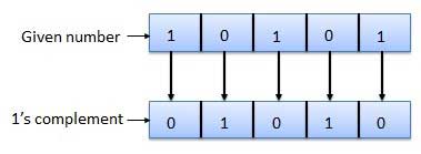
1's complement
2's complement
- It is obtained by adding 1 to the Least Significant Bit (LSB) of 1's complement of the number.
- Hence, 2's complement = 1's complement + 1
- For Example:
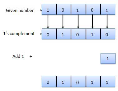
2's complement
Binary to Hexadecimal
- Dividing the binary digits into groups of four (starting from right to left).
- Then converting each group of four binary digits into one hexadecimal number.
For example:
Binary Number − 101012
Its hexadecimal Equivalent –
Step | Binary Number | Hexadecimal Number |
Step 1 | 101012 | 0001 0101 |
Step 2 | 101012 | 110 510 |
Step 3 | 101012 | 1516 |
Binary Number − 101012 = Hexadecimal Number − 1516
Hexadecimal to Binary
- Converting each hexadecimal digit to a 4 digit binary number and they can be treated as decimal number.
- Combining all the resulting binary groups into a single binary number.
For example:
Hexadecimal Number − 1516
Its Binary Equivalent –
Step | Hexadecimal Number | Binary Number |
Step 1 | 1516 | 110 510 |
Step 2 | 1516 | 00012 01012 |
Step 3 | 1516 | 000101012 |
Hexadecimal Number − 1516 = Binary Number − 101012
- In coding, when alpha-numeric characters or words are represented by a specific group of symbols, it is said that it is being coded.
- The group of symbols is known as a code.
- The digital data can be represented, stored and transmitted as group of binary bits.
- This group is called as binary code.
- It is represented by the number as well as alphanumeric character.
Advantages of Binary Code
- They are used in computer applications.
- They are suitable for digital communications.
- They make the analysis and designing of digital circuits easy.
- Implementation becomes very easy since only 0 & 1 are being used.
Classification of binary codes
The codes are broadly classified as:
- Weighted Codes
- Non-Weighted Codes
- Binary Coded Decimal Code
- Alphanumeric Codes
- Error Detecting Codes
- Error Correcting Codes
Weighted Codes
- These codes obey the positional weight principle.
- Here each position represents a specific weight.
- Several systems are used to express the decimal digits 0 through 9.
- Here, each decimal digit is represented by a set of four bits.
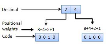
Fig: Weighted codes
Non-Weighted Codes
- Here, the positional weights are not assigned.
- Example: Excess-3 code and Gray code.
1.Excess-3 code
- It is also known as XS-3 code.
- It is a non-weighted code used to express decimal numbers.
- They are derived from the 8421 BCD code words adding (0011)2 or (3)10 to each code word in 8421.
- The excess-3 codes are obtained as −

Example
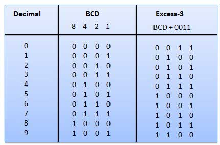
Fig: BCD to XS 3 conversion
2.Gray Code
- It is the non-weighted code and is not an arithmetic code.
- This means that there are no specific weights assigned to the bit position.
- Here only one bit will change every time the decimal number is incremented.
- The gray code is also known as a unit distance code as only one bit changes at a time.
- The gray code is a type of cyclic code.
- It cannot be used for all arithmetic operation.
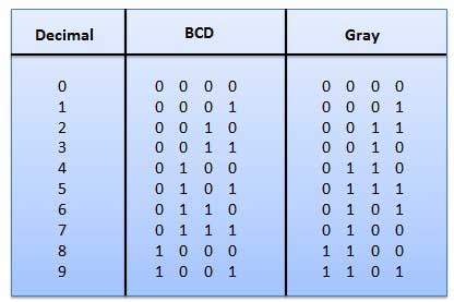
Fig: Gray codes
Application of Gray code
- They are used in the shaft position encoders.
- This encoder produces a code word which represents the angular position of the shaft.
3. Binary Coded Decimal (BCD) code
- Here each decimal digit is represented by a 4-bit binary number.
- Its a way to express each of the decimal digits with a binary code.
- Therefore, by four bits we can represent sixteen numbers (0000 to 1111).
- But in BCD code only first ten of these numbers are used (0000 to 1001) and rest are invalid.

Fig: BCD codes
Advantages of BCD Codes
- It is very similar to decimal system.
- We have to remember binary equivalent of 0 to 9 only.
Disadvantages of BCD Codes
- The addition and subtraction of BCD number system have different rules.
- The BCD arithmetic is more complicated.
- BCD code requires more number of bits than binary code to represent the decimal number.
- Hence is less efficient than binary.
4. Alphanumeric codes
A binary digit or bit can be represented by two symbols as '0' or '1'.
This is not sufficient for communication between two computers as we need many more symbols for communication.
These symbols are represents 26 alphabetic characters with capital and small letters, numbers from 0 to 9, punctuation marks and other symbols.
These alphanumeric codes represent numbers and alphabetic characters.
Most of them also represent other characters like symbol and various instructions necessary for conveying information.
The code at least represents 10 digits and 26 letters of alphabet i.e. total 36 items.
The following three types of alphanumeric codes are commonly used for the data representation.
- American Standard Code for Information Interchange (ASCII).
- Extended Binary Coded Decimal Interchange Code (EBCDIC).
- Five bit Baudot Code.
ASCII code is a 7-bit code whereas EBCDIC is an 8-bit code.
ASCII code is used worldwide while EBCDIC is primarily used in large IBM computers.
5. Error Codes
There technique is available to detect and correct data during data transmission.
Error Code | Description |
Error Detection and Correction | Error detection and correction code techniques |
Codes Conversion
Various conversion techniques are:
- Binary to BCD Conversion
- BCD to Binary Conversion
- BCD to Excess-3
- Excess-3 to BCD
Binary to BCD Conversion
- Converting the binary number to its decimal equivalent.
- Then converting the decimal number to its equivalent BCD.
For Example –
Convert (11101)2 to BCD.
Step 1 − Convert to Decimal
Binary Number − 111012
Its Decimal Equivalent –
Step | Binary Number | Decimal Number |
Step 1 | 111002 | ((1 × 24) + (1 × 23) + (1 × 22) + (0 × 21) + (0 × 20))10 |
Step 2 | 111002 | (16 + 8 + 4 + 0 + 0)10 |
Step 3 | 111002 | 2810 |
Binary Number − 111002 = Decimal Number − 2810
Step 2 -- Convert to BCD
Decimal Number − 2810
Its BCD Equivalent:
Step | Decimal Number | Conversion |
Step 1 | 2810 | 00102 10002 |
Step 2 | 2810 | 00101000BCD |
Result
(11100)2 = (00101000)BCD
BCD to Binary Conversion
- Converting the BCD number to decimal equivalent.
- Then converting decimal to binary equivalent.
For Example –
Convert (00101001)BCD to Binary.
Step 1 - Converting to BCD
BCD Number − (00101001)BCD
Its Decimal Equivalent.
Step | BCD Number | Conversion |
Step 1 | (00101001)BCD | 00102 10012 |
Step 2 | (00101001)BCD | 210 910 |
Step 3 | (00101001)BCD | 2910 |
Step 2 - BCD Number − (00101001)BCD = Decimal Number − 2910
Converting to Binary by Using long division method.
Decimal Number − 2910
Calculating Binary Equivalent –
Step | Operation | Result | Remainder |
Step 1 | 29 / 2 | 14 | 1 |
Step 2 | 14 / 2 | 7 | 0 |
Step 3 | 7 / 2 | 3 | 1 |
Step 4 | 3 / 2 | 1 | 1 |
Step 5 | 1 / 2 | 0 | 1 |
So, Decimal Number − 2910 = Binary Number − 111012
Result
(00101001)BCD = (11101)2
BCD to Excess-3
- Converting BCD to decimal equivalent.
- Adding (3)10 to this decimal number.
- Then converting into binary to get the required excess-3 code.
For Example –
Convert (1000)BCD to Excess-3.
Step 1 − Convert to decimal
(1000)BCD = 810
Step 2 − Add 3 to decimal
(8)10 + (3)10 = (11)10
Step 3 − Convert to Excess-3
(11)10 = (1011)2
Result
(1000)BCD = (1011)XS-3
Excess-3 to BCD Conversion
- Subtracting (0011)2 from each 4 bit of excess-3 digit to obtain the corresponding BCD code.
For Example –
Convert (10011000)XS-3 to BCD.
Given XS-3 number = 1 0 0 1 1 0 0 0

Result
(10011000)XS-3 = (01100101)BCD
Errors and Error Correcting Codes
- When bits are being transmitted over the computer network, they get corrupted due to interference and network problems.
- These corrupted bits leads to spurious data that is being received by the receiver and are called errors.
- Hence the Error-correcting codes (ECC) are a sequence of numbers which are generated by specific algorithms for detecting and removing errors in data that can be transmitted over various noisy channels.
- They ascertain the exact number of bits that has been corrupted and the also their location in algorithm.
ECCs are of two types −
- Block codes − The message is divided into fixed-sized blocks of bits which are added for error detection or correction.
- Convolutional codes − The message consists of data streams of arbitrary length and parity symbols are being generated by sliding the application of a Boolean function to the data stream.
- Computers are digital in nature.
- They process, store, and communicate information in binary form which is the combination of 1s and 0s.
- A bit is an individual 1 or O.
- Multiple bit streams are used in a computer network.
- Here, signal varies in voltage to positive (+) voltage and a null or zero (0) voltage (unipolar) or a positive (+) or a negative (-) voltage (bipolar).

- Digital electronic circuits operate at two logic levels namely Logic Low and Logic High.
- The Logic Low is represented with ‘0’and Logic High is represented with ‘1’.
- The basic digital electronic circuit which has one or more inputs and single output is known as Logic gate.
- These Logic gates are known as the building blocks of any digital system. They can classified as:
- Basic gates
- Universal gates
- Special gates
- NAND & NOR gates are known as universal gates.
- We can implement any Boolean function by using NAND gates and NOR gates alone.
NAND gate
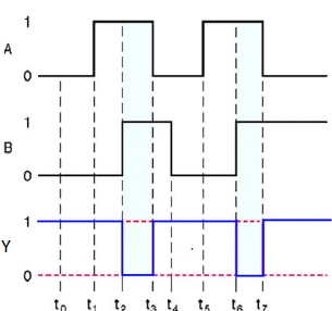
It is a digital circuit which has two or more inputs and single output and it is the inversion of logical AND gate.
The truth table of 2-input NAND gate is:
A | B | Y = (A.B)’ |
0 | 0 | 1 |
0 | 1 | 1 |
1 | 0 | 1 |
1 | 1 | 0 |
Here A, B are the inputs and Y is the output of two input NAND gate. When both inputs are ‘1’, then the output, Y is ‘0’. If at least one of the input is zero, then the output, Y is ‘1’. This is just the inverse of AND operation.
The image shows the symbol of NAND gate:

Fig.: NAND gate (ref. 1)
NAND gate works same as AND gate followed by an inverter.
Timing Diagram:
NOR gate
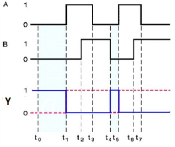
It is a digital circuit that has two or more inputs and a single output which is the inversion of logical OR of all inputs.
The truth table of 2-input NOR gate is:
A | B | Y = (A+B)’ |
0 | 0 | 1 |
0 | 1 | 0 |
1 | 0 | 0 |
1 | 1 | 0 |
Here A and B are the two inputs and Y is the output. If both inputs are ‘0’, then the output is ‘1’. If any one of the input is ‘1’, then the output is ‘0’. This is exactly opposite to two input OR gate operation.
The symbol of NOR gate is:

Fig.: NOR gate (ref. 1)
NOR gate works exactly same as that of OR gate followed by an inverter.
Timing Diagram:
Special Gates
Ex-OR gate
It stands for Exclusive-OR gate. Its function varies when the inputs have even number of ones.
The truth table of 2-input Ex-OR gate is:
A | B | Y = A⊕B |
0 | 0 | 0 |
0 | 1 | 1 |
1 | 0 | 1 |
1 | 1 | 0 |
Here A, B are the inputs and Y is the output of two input Ex-OR gate. The output (Y) is zero instead of one when both the inputs are one.
Therefore, the output of Ex-OR gate is ‘1’, when only one of the two inputs is ‘1’. And it is zero, when both inputs are same.
The symbol of Ex-OR gate is as follows:
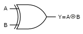
Fig.: XOR gate (ref. 1)
It is similar to that of OR gate with an exception for few combination(s) of inputs. Hence, the output is also known as an odd function.
Timing Diagram:

Ex-NOR gate
It stands for Exclusive-NOR gate. Its function is same as that of NOR gate except when the inputs having even number of ones.
The truth table of 2-input Ex-NOR gate is:
A | B | Y = A⊙B |
0 | 0 | 1 |
0 | 1 | 0 |
1 | 0 | 0 |
1 | 1 | 1 |
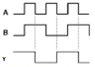
Here A, B are the inputs and Y is the output. It is same as Ex-NOR gate with the only modification in the fourth row. The output is 1 instead of 0, when both the inputs are one.
Hence the output of Ex-NOR gate is ‘1’, when both inputs are same and 0, when both the inputs are different.
The symbol of Ex-NOR gate is:
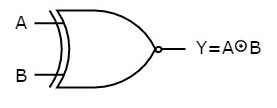
Fig.: XNOR gate (ref. 1)
It is similar to NOR gate except for few combination(s) of inputs. Here the output is ‘1’, when even number of 1 is present at the inputs. Hence is also called as an even function.
Timing Diagram:
The three basic laws of Boolean Algebra are:
- Commutative law
- Associative law
- Distributive law
Commutative Law
- The logical operation carried between two Boolean variables when gives the same result irrespective of the order the two variables, then that operation is said to be Commutative. The logical OR & logical AND operations between x & y are shown below
x + y = y + x
x.y = y.x
- The symbol ‘+’ and ‘.’ indicates logical OR operation and logical AND operation.
- Commutative law holds good for logical OR & logical AND operations.
Associative Law
- If a logical OR operation of any two Boolean variables is performed first and then the same operation is performed with the remaining variable providing the same result, then that operation is said to be Associative. The logical OR & logical AND operations of x, y & z are:
x + (y + z) = (x + y) + z
x.(y.z) = (x.y).z
- Associative law holds good for logical OR & logical AND operations.
Distributive Law
- If a logical OR operation of any two Boolean variables is performed first and then AND operation is performed with the remaining variable, then that logical operation is said to be Distributive. The distribution of logical OR & logical AND operations between variables x, y & z are :
x.(y + z) = x.y + x.z
x + (y.z) = (x + y).(x + z)
- Distributive law holds good for logical OR and logical AND operations.
- These are the Basic laws of Boolean algebra and we can verify them by substituting the Boolean variables with ‘0’ or ‘1’.
TTL
1) Transistor-transistor logic (TTL) is a class of integrated circuits that maintains logic states and switches with the help of bipolar transistors.
2) It inputs rise to the logic "1" if left unconnected. It is one of the reasons that integrated circuits are widely used, as they are cheap, reliable and faster than RTL and DTL.
3) TTL makes use of transistors with multiple emitters in gates having multiple inputs.
4) The family of TTL is as follows:
- Standard TTL
It is used for 3.3-volt power supplies and memory interfacing.
- Fast TTL
It has faster switching than (6ns) but significantly higher power dissipation (22 mW).
- Schottky TTL
It uses Schottky diode clamps at gate inputs to prevent charge storage and improve switching time.
- Low power Schottky TTL
It is used for high resistance values of low-power TTL and the Schottky diodes provide a good combination of speed (9.5ns) and reduce power consumption (2 mW) too.
- Low power TTL
It is traded switching speed (33ns) for a reduction in power consumption (1 mW).
- Advanced Schottky TTL
It speeds up the low-to-high transition of TTL.
Advantages
- It is relatively easy in interfacing different circuits and produce complex logic functions.
- It has good noise margins as well as guaranteed voltage levels.
- It has good fan-in and is largely immune to damage from static electricity discharges
Disadvantages
- It has limited speed, low frequency, very noisy, high power consumption at higher frequencies.
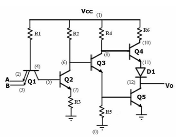
Fig. TTL
CMOS logic
1) The MOSFET (metal-oxide-semiconductor field-effect transistor) are of two types: PMOS (p-type MOS) and NMOS (n-type MOS).
2) A new type of MOSFET logic is made combining both the PMOS and NMOS processes and is called as complementary MOS (CMOS).
3) CMOS stands for “Complementary Metal Oxide Semiconductor”.
4) It is one of the most popular technology in the chip design industry and is used today to form integrated circuits or various applications.
5) Computer memories, CPUs and cell phones make use of this technology due to various advantages. This technology uses both P and N channel semiconductor devices.
CMOS Applications
- Computer memories, CPUs
- Microprocessor designs
- Flash memory chip designing
- Used to design application specific integrated circuits (ASICs)
Advantages
- The power dissipation is very small.
- Greater number of IC’s can be integrated on a single chip.

Fig. CMOS
CMOS
- CMOS stands for “Complementary Metal Oxide Semiconductor”.
- Computer memories, CPUs and cell phones make use of this technology due to various advantages. This technology uses both P and N channel semiconductor devices.
TTL
- TTL is a standard method of construction for the processors of mini-computer and mainframe processors.
- TTL gate works as an analog amplifier.
In digital electronics three-state, tri-state, or 3-state logic allows an output port to assume a high impedance state, effectively removing the output from the circuit, in addition to the 0 and 1 logic levels.
INPUT | OUTPUT |
|
A | B | C |
0 | 0 | Z (high impedance) |
1 | 0 | Z (high impedance) |
0 | 1 | 0 |
1 | 1 | 1 |

References:
1. R. P. Jain, "Modern Digital Electronics", McGraw Hill Education, 2009.
2. M. M. Mano, "Digital logic and Computer design", Pearson Education India, 2016.
3. A. Kumar, "Fundamentals of Digital Circuits", Prentice Hall India, 2016.
4. Thomas C Bartee, “Digital Computer Fundamentals”,McGraw Hill,1985.
5. Herbert Taub, Donald LSchilling “Digital Integrated Electronics”, McGraw Hill, 1977