Unit - 5
Semiconductor memories and Programmable logic devices
The memory is organized in the form of a cell, each cell is able to be identified with a unique number called address. Each cell is able to recognize control signals such as “read” and “write”, generated by CPU when it wants to read or write address. Whenever CPU executes the program there is a need to transfer the instruction from the memory to CPU because the program is available in memory. To access the instruction CPU generates the memory request.
Memory Request:
Memory request contains the address along with the control signals. For Example, When inserting data into the stack, each block consumes memory (RAM) and the number of memory cells can be determined by the capacity of a memory chip.
Example: Find the total number of cells in 64k*8 memory chip.
Size of each cell = 8
Number of bytes in 64k = (26)*(210)
Therefore,
The total number of cells = 216 cells
With the number of cells, the number of address lines required to enable one cell can be determined.
Word Size:
It is the maximum number of bits that a CPU can process at a time and it depends upon the processor. Word size is a fixed size piece of data handled as a unit by the instruction set or the hardware of a processor.

Expanded memory is addressed from within the lower 1MB space, usually above 640K. It is sometimes up to 64K of real addresses but this is just a small portion of the whole expanded memory, which can be very large. The expanded memory requires hardware and/or software that maps the expanded memory to a piece of address space, in what is called a "page frame". Extended memory can be used as expanded memory by using software and the 80286 or 80386 chips to "remap" it to the lower 1MB.
Memory can be classified as –
- Main Memory– Main memory has the disadvantage of high-cost and low-capacity storage. But its advantage or facility is the high speed of data transfer. The control unit can be able to directly communicate with the main memory. Main memory can be generally classified into random-access memory (RAM) and read-only memory (ROM). It is a volatile memory. Due to the absence of power, the content of this memory will be lost.
- Secondary Memory– Secondary memory is also frequently known as auxiliary memory. The control unit can’t directly communicate with the secondary memory. It is a non-volatile memory.
Random Access Memory (RAM) – RAM contains of a various number of memory locations wherein each location typically 8-bits are stored. It can be possible to read from a RAM location, as well as write to a RAM location. The drawback of RAM is that it is volatile. That means, when the power supply to the RAM is switched off, the information in the RAM will be lost.
From the memory, data can be accessed in two different ways – Sequential Access and Random Access.
Sequential Access − Sequential access and random access are two types of accessing information. In sequential access, it is mandatory to access information strictly in order. If there are 4000 memory locations, it has to be accessed in the order of 1, 2, 3,…,4000. Thus, it takes minimum time to access information from location 0 and at most time to access information from location 4000. Magnetic Tape is an example that employs sequential access.
Random Access − In a random-access technique, it can be possible to access a memory location in any order. For example, one can read from the 4000locations in the order of 1500, 1210, 3060, 1640, 1352, and so on. Second, it takes a similar time to read from a memory location irrespective of its position. In a RAM, the access method is random, and its name, in fact, is derived based on the method of access.
Read Only Memory (ROM) – ROM consists of a number of memory locations wherein each location typically 8-bits are stored like a RAM. A ROM also uses random access method just like a RAM. The advantage of ROM is that it is non-volatile in nature.
The different versions of ROM which are provided by semiconductor manufacturers for storing information –
Mask-Programmed ROM – It derives this name because the information is written to this type of ROM at the time of manufacture by applying a suitable mask. Once the manufacturer writes this type of ROM, it cannot be possible to change this information even by the manufacturer. So that the information entered is permanent. It is cheap with compared to the other types of ROMs when the cost per unit quantity is considered.
Programmable Read Only Memory (PROM) – The user writes information to this type of ROM with the help of PROM programmer equipment. Once the user writes this type of ROM, it cannot be possible to change this information anymore. Like Mask-Programmed ROM, the information entered is permanent. Though itis cheaper than the other types of ROMs but it is costlier than a mask ROM. The user can buy even a single piece of PROM from a local shop. Thus, PROMs are implemented in equipment those are produced in small quantities.
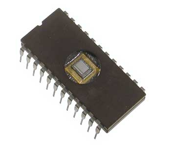
Erasable Programmable Read Only Memory (EPROM) – Information is written to this type of ROM by the user with the help of EPROM programmer equipment. As its content is erasable and rewritable, so the user can change this information in a number of times. Thus, although the information entered is not lost when power is switched off, it can be possible to erase it and then write new information. With the exposure of strong ultraviolet (UV) light from a very close distance on the quartz window of the EPROM chip, we can erase the content of the EPROM. Then the contents of the entire EPROM are entirely lost. The user can purchase even a single piece of EPROM from the market read and write its content for several numbers of times as well.
Electrically erasable (or Alterable) Programmable Read Only Memory (EEPROM or EEPROM) − Information is has written to this type of ROM by the user with the help of EPROM programmer equipment. After the user writes this type of ROM, it can be possible to change this information a number of times.
Sequential Memory
Sequential access memory (SAM) is a class of data storage devices that read stored data in a sequence. This is in contrast to random access memory (RAM) where data can be accessed in any order. Sequential access devices are usually a form of magnetic storage or optical storage.
While sequential access memory is read in sequence, arbitrary locations can still be accessed by "seeking" to the requested location. This operation, however, is often relatively inefficient (see seek time, rotational latency).
Magnetic sequential access memory is typically used for secondary storage in general-purpose computers due to their higher density at lower cost compared to RAM, as well as resistance to wear and non-volatility. Magnetic tape is a type of sequential access memory still in use; historically, drum memory has also been used.
Read Only Memory (ROM)
- ROM stands for Read Only Memory.
- It can only read but cannot write on it.
- This memory is non-volatile.
- The information is stored permanently during manufacturing.
- It stores instructions that are required to start a computer and is referred to as bootstrap.
- They are not only used in the computer but also in other electronic devices like washing machine, microwave oven etc.
Advantages:
- Non-volatile in nature
- Cheaper than RAMs
- Easy to test
- More reliable
Types:
- Programmable Read-Only Memory (PROM)
- Electrically Programmable Read-Only Memory (EPROM)
- Electrically Erasable Programmable Read-Only Memory (EEPROM; also called Flash ROM)
- Electrically Alterable Read-Only Memory (EAROM)
They are often referred to as programmable ROM. It was designed for specific data which contains the start-up code.
Key Takeaways:
- ROM can only read but cannot write.
- This memory is non-volatile and information is stored permanently.
Read and Write Memory (RAM)
- RAM (Random Access Memory) is the internal memory of the CPU which is used for storing data, program, and result. It is a read-write memory which stores data only if the machine is working and as the machine is switched off, data gets erased.
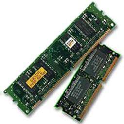
- Access time is independent of the address hence each storage location inside the memory is easy to reach and takes the same amount of time. Here, Data can be accessed randomly and is very expensive.
- RAM is volatile in nature therefore data stored in it is lost when we switch off the computer or in case of power failure.
- Hence, a Uninterruptible Power System (UPS) is used as a backup with computers. RAM is small in size and in the amount of data it can hold.
Content Addressable Memory (CAM)
Content-addressable memory (CAM) is silicon chip architecture that is purpose-built for extremely fast but very specific type of memory lookups. Lookups using a CAM is conceptually similar to associative array logic in data structures but the output are highly simplified. When key is passed to a CAM sub-system it returns the associated value to that key. As a result, a “key -> value” pair is created that can be referenced further as an object. The most important feature is that a lookup of an entry in a CAM can be performed in a single clock cycle in the silicon. Compare this with a RAM module that requires multiple clock cycles to make a single memory fetch.
Charge De Coupled Device Memory (CCD)
A charge coupled device (CCD) is an integrated circuit etched onto a silicon surface forming light sensitive elements called pixels. Photons incident on this surface generate charge that can be read by electronics and turned into a digital copy of the light patterns falling on the device. CCDs come in a wide variety of sizes and types and are used in many applications from cell phone cameras to high-end scientific applications.
There are a few different types of memory chips:
- Dynamic random-access memory (DRAM) chips: Also known as volatile memory chips because they lose memory once the power supply is removed. DRAM can only transmit a single line of memory and needs to be constantly refreshed to prevent the loss of memory bits.
- Static random-access memory (SRAM) chips: Non-volatile chips that are commonly used in portable battery-powered devices. Unlike DRAM, they do not need to be refreshed and do not immediately lose memory when the power source is disconnected.
- First in, first out (FIFO) memory chips: Mainly used when memory is being transferred between different types of devices.
- Erasable programmable read only memory (EPROM): The memory in these chips can be erased when exposed to ultraviolet rays. These chips can then be reprogrammed for a new set of data values.
- Programmable read only memory (PROM) memory: Differs from other programmable memory chips as they can only be programmed once. The contents cannot be erased electronically or though ultraviolet rays.
If the ROM has programmable feature, then it is called as Programmable ROM PROM. The user has the flexibility to program the binary information electrically once by using PROM programmer. PROM is a programmable logic device that has fixed AND array & Programmable OR array.
- Programmable Logic Array (PLA) is a fixed architecture logic device with programmable AND gates followed by programmable OR gates.
- It is basically a type of programmable logic device used to build reconfigurable digital circuit.
- PLDs have undefined function at the time of manufacturing but they are programmed before made into use.
- PLA is a combination of memory and logic.
- PLA is similar to a ROM in concept; however it does not provide full decoding of variables and does not generate all min terms as in the ROM.
- It does not require any type of programming like in C and C++.
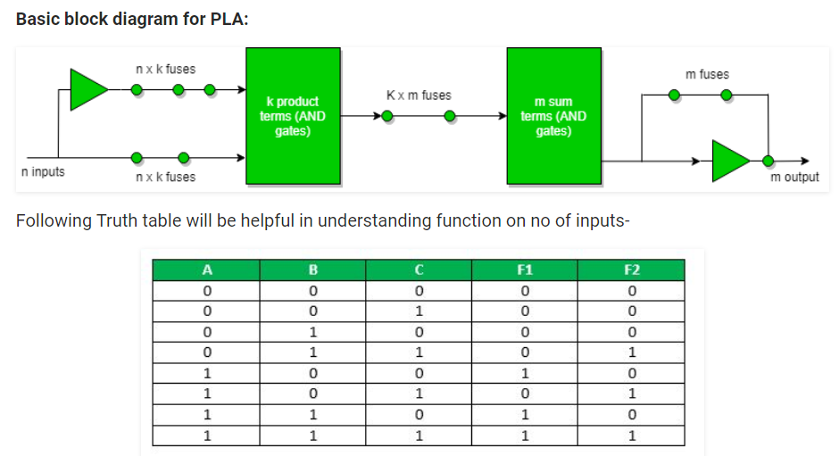
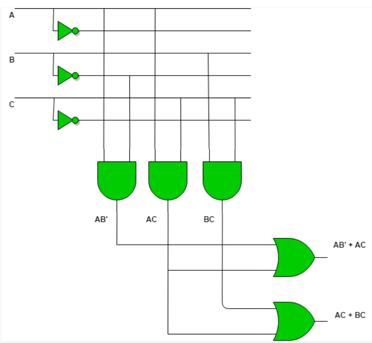
F1 = AB’C’ + AB’C + ABC’ + ABC
On simplifying we get : F1 = AB’ + AC
F2 = A’BC + AB’C + ABC
On simplifying we get: F2 = BC + AC
Applications:
- PLA is used to provide control over data path.
- PLA is used as a counter.
- PLA is used as a decoder.
- PLA is used as a BUS interface in programmed I/O.
- PAL stands for Programmable Array Logic.
- It is one type of PLD which is known as Programmable Logic Device circuit, and working of this PAL is the same as the PLA.
- The designing of the PAL can be done with fixed OR gates as well as programmable AND gates. By using this we can implement two easy functions wherever the associates AND gates with each OR gate denote the highest number of product conditions that can be produced in the form of SOP (sum of product) of an exact function.
- As the logic gates like AND is connected continually toward the OR gates, and that indicates that the produced product term is not distributed with the output functions.
- The major notion behind PLD development is to fabricate a compound Boolean logic onto a single chip by removing the defective wiring, avoiding the logic design, as well as decreasing the consumption of power.
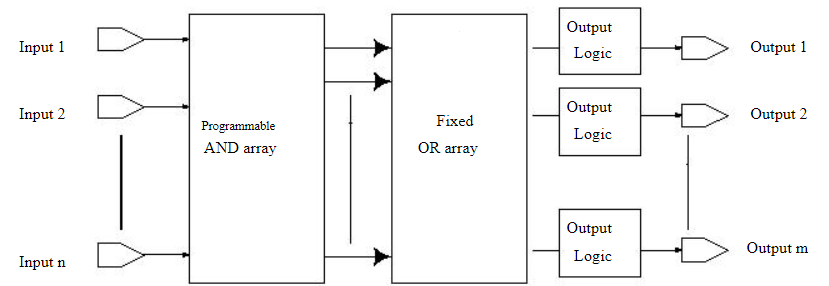
Fig.: PAL architecture
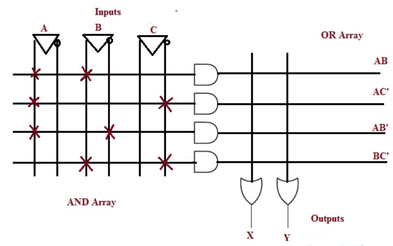
Implement the following Boolean expression with the help of programmable array logic (PAL)
X =AB + AC’
Y= AB’ + BC’
Applications:
- PAL is used as a counter.
- PAL is used as a decoders.
Comparison between PLA and PAL
Programmable Array Logic (PAL) | Programmable Logic Array (PLA) |
The full form of PAL is programmable array logic | The full form of the PLA is a programmable logic array |
The construction of PAL can be done using the programmable collection of AND & OR gates | The construction of PLA can be done using the programmable collection of AND & fixed collection of OR gates. |
The availability of PAL is less prolific | The availability of PLA is more |
The flexibility of PAL programming is more | The flexibility of PLA is less |
The cost of a PAL is expensive | The cost of PLA is middle range |
The number of functions implemented in PAL is large | The number of functions implemented in PLA is limited |
The speed of PAL is slow | The speed of PLA is high |
A complex programmable logic device comprises of a group of programmable FBs (functional blocks). The inputs and outputs of these functional blocks are connected together by a GIM (global interconnection matrix). This interconnection matrix is reconfigurable, so that we can modify the contacts between the functional blocks. There will be some input and output blocks that let us to unite CPLD to external world. The architecture of CPLD is shown below.
Generally, the programmable FB looks like the array of logic gates, where an array of AND gates can be programmed and OR gates are stable. But, each manufacturer has their way of thinking to design the functional block. A listed o/p can be found by operating the feedback signals attained from the OR gate outputs.

Fig.: CPLD architecture
In CPLD programming, the design is first coded in Verilog or VHDL language once the code is (simulated and synthesized. During synthesis, the CPLD model (target device) is handpicked and a technology-based mapping net list is produced. This list can be close-fitting to the genuine CPLD architecture using a place and route process, typically achieved by the place-and-route software of CPLD Company’s proprietary. Then the operator will do some confirmation processes. If everything is good, he will utilize the CPLD, else he will rearrange it.
The field-programmable gate array (FPGA) is an integrated circuit that consists of internal hardware blocks with user-programmable interconnects to customize operation for a specific application.
FPGA architecture consists of thousands of fundamental elements called configurable logic blocks (CLBs) surrounded by a system of programmable interconnects, called a fabric, that routes signals between CLBs. Input/output (I/O) blocks interface between the FPGA and external devices.
Depending on the manufacturer, the CLB may also be referred to as a logic block (LB), a logic element (LE) or a logic cell (LC).

Fig.: FPGA architecture
An individual CLB is made up of several logic blocks. A lookup table (LUT) is a characteristic feature of an FPGA. An LUT stores a predefined list of logic outputs for any combination of inputs: LUTs with four to six input bits are widely used. Standard logic functions such as multiplexers (mux), full adders (FAs) and flip-flops are also common.
The number and arrangement of components in the CLB varies by device.
It contains two three-input LUTs an FA and a D-type flip-flop plus a standard mux and two muxes, that are configured during FPGA programming.
This simplified CLB has two modes of operation. In normal mode, the LUTs are combined with Mux 2 to form a four-input LUT; in arithmetic mode, the LUT outputs are fed as inputs to the FA together with a carry input from another CLB.
Current-generation FPGAs include more complex CLBs capable of multiple operations with a single block; CLBs can combine for more complex operations such as multipliers, registers, counters and even digital signal processing (DSP) functions.
Compare CPLD and FPGA
| CDLD | FPGA |
1 | Instant-on. CPLDs start working as soon as they are powered up | Since FPGA has to load configuration data from external ROM and setup the fabric before it can start functioning, there is a time delay between power ON and FPGA starts working. The time delay can be as large as several tens of milliseconds. |
2 | Non-volatile. CPLDs remain programmed, and retain their circuit after powering down. FPGAs go blank as soon as powered-off. | FPGAs uses SRAM based configuration storage. The contents of the memory is lost as soon as power is disconnected. |
3 | Deterministic Timing Analysis. Since CPLDs are comparatively simpler to FPGAs, and the number of interconnects are less, the timing analysis can be done much more easily. | Size and complexity of FPGA logic can be humongous compared to CPLDs. This opens up the possibility less deterministic signal routing and thus causing complicated timing scenarios. Thankfully implementation tools provided by FPGA vendors have mechanisms to assist achieving deterministic timing. But additional steps by the user is usually necessary to achieve this. |
4 | Lower idle power consumption. Newer CPLDs such as CoolRunner-II use around 50 uA in idle conditions. | Relatively higher idle power consumption. |
5 | Might be cheaper for implementing simpler circuits | FPGAs are much more capable compared to CPLDs but can be more expensive as well. |
6 | More "secure" due to design storage within built in non-volatile memory. | FPGAs that use external memory can expose the IP externally. Many FPGA vendors offer mechanisms such as encryption to combat this. Design specific protection mechanisms also can be implemented. |
7 | Very small amount of logic resources. | Massive amount logic and storage elements, with which incredibly complex circuits can be designed. FPGAs have thousands of times more resources! This point alone makes FPGAs more popular than CPLDs. |
8 | No on-die hard IPs available to offload processing from the logic fabric. | Variety of on-die dedicated hardware such as Block RAM, DSP blocks, PLL, DCMs, Memory Controllers, Multi-Gigabit Transceivers etc give immense flexibility. This is not even thinkable with CPLDs. |
9 | Power down and reprogramming is always required in order to modify design functionality. | FPGAs can change their circuit even while running! (Since it is just a matter of updating LUTs with different content) This is called Partial Reconfiguration, and is very useful when FPGAs need to keep running a design and at the same time update the it with different design as per requirement. This feature is widely used in Accelerated Computing. |
References:
1. R. P. Jain, "Modern Digital Electronics", McGraw Hill Education, 2009.
2. M. M. Mano, "Digital logic and Computer design", Pearson Education India, 2016.
3. A. Kumar, "Fundamentals of Digital Circuits", Prentice Hall India, 2016.
4. Thomas C Bartee, “Digital Computer Fundamentals”, McGraw Hill,1985.
5. Herbert Taub, Donald LSchilling “Digital Integrated Electronics”, McGraw Hill, 1977