Unit - 2
Combinational Circuit
An arithmetic circuit is a set of gates with a separate set of inputs for each number that has to be processed. The gates are connected so as to carry out an arithmetic action and the outputs of the gate circuit are the digits of the result (addition, subtraction, multiplication, or division).
Half Adder
It is a combinational circuit which has two inputs and two outputs.
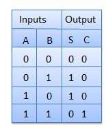
It is designed to add two single bit binary number A and B.
It has two outputs carry and sum.
Block diagram
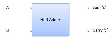
Fig. Half adder
Truth Table
Circuit Diagram
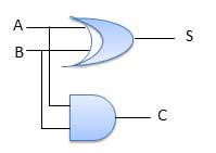
Fig. Half adder
Full Adder
- It is developed to overcome the drawback of Half Adder circuit.
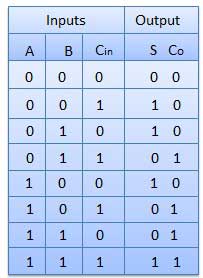
- It can add two one-bit numbers A and B and a carry C.
- It is a three input and two output combinational circuit.
Block diagram
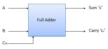
Fig. Full adder
Truth Table
Circuit Diagram
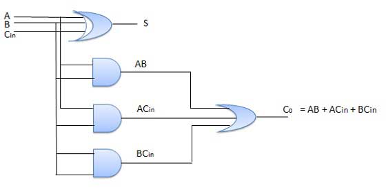
Fig. Full adder
Key Takeaways:
- Half adder is a combinational circuit which has two inputs and two outputs.
- Since there is no provision for carry in half adder, full adder is developed to overcome the drawback.
Subtractor
Half Subtractors
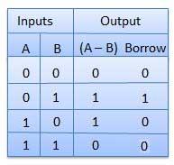
It is a combination circuit with two inputs and two outputs.
The difference between the two binary bits is obtained at the output and an output (Borrow) indicates if a 1 has been borrowed.
Here A is called as Minuend bit and B is called as Subtrahend bit.
Truth Table
Circuit Diagram
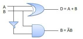
Fig. Half subtractor
Full Subtractors
It is a combinational circuit which has three inputs A,B,C and two output D and C'.
A is the 'minuend', B is 'subtrahend', C is the 'borrow' which is produced by the previous stage, difference output D and C' is the borrow output.
Truth Table
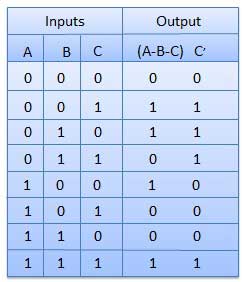
Circuit Diagram
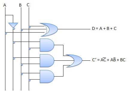
Fig. Full subtractor
Key Takeaways:
- Half subtractor is a combinational circuit which has two inputs and two outputs.
- Since there is no provision for borrow in half subtractor, full subtractor is developed to overcome the drawback.
- An ALU performs mathematical and logical operations on binary numbers.
- They are located at the heart of every digital computer system and are one of the most important parts of a CPU (Central Processing Unit).
- Fetch-decode-execute refers to a computational process that continuously fetches the instructions from a memory, decodes them into operations and executes them to perform a calculation.
- These are simple steps which give rise to the complex behaviours that we expect from modern computing machines.
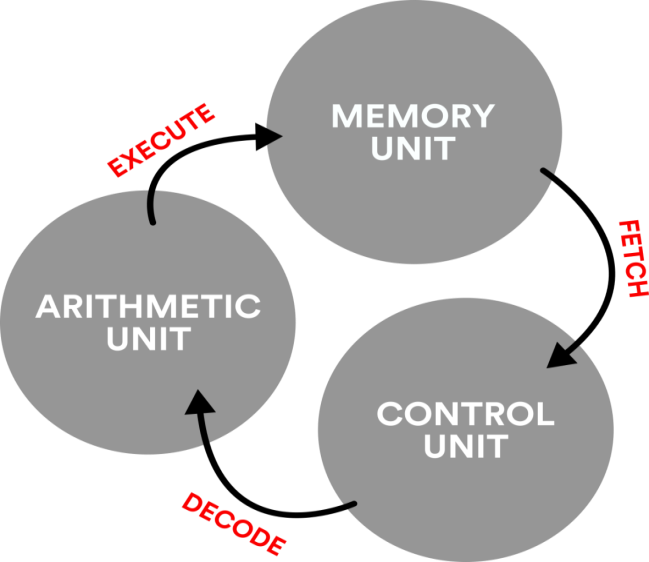
Fig. An illustration of the fetch-decode-execute cycle
This process can be further explained by linking each cycle step with three hardware subsystems called as a memory unit, a control unit, and an arithmetic unit.
- It performs comparison operation with more than four bits by cascading two or more 4-bit comparators.
- When two comparators are to be cascaded, the outputs of the lower-order comparator is connected to corresponding input of the higher-order comparator.
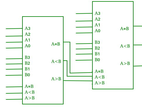
Fig. Digital comparator
Applications of Comparators –
- They are used in central processing units (CPUs) and microcontrollers (MCUs).
- They are used in control applications where the binary numbers represents physical variables such as temperature, position, etc. and are compared with a reference value.
- They are also used as process controllers and Servo motor controllers.
- They are used in password verification and biometric applications too.
- The parity generating technique is used as error detection technique for the data transmission.
- When binary data is transmitted and processed , it is subjected to noise and that noise can alter 0s to 1s and 1s to 0s of data bits in digital systems.
- Therefore, a parity generator is a combinational logic circuit that generates the parity bit at the transmitter end.
- The basic principle is that sum of odd number of 1s is always 1 and sum of even number of 1s is always zero.
- Such error detection and correction can be implemented by using Ex-OR gates.
Even Parity Generator
A 3-bit message is transmitted with an even parity bit. Hence assuming, the three inputs W,X and Y that are applied to the circuits and output bit is the parity bit P. The total number of 1s must be even, to generate the even parity bit P.
3- bit message | Even Parity | ||
W | X | Y | P |
0 | 0 | 0 | 0 |
0 | 0 | 1 | 1 |
0 | 1 | 0 | 1 |
0 | 1 | 1 | 0 |
1 | 0 | 0 | 1 |
1 | 0 | 1 | 0 |
1 | 1 | 0 | 0 |
1 | 1 | 1 | 1 |
The K-map simplification for 3-bit message even parity generator is
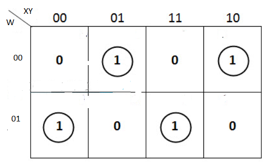
From the above K-Map, the expression is:
P=W′X′Y+W′XY′+WX′Y′+WXY
P=W′(X′Y+XY′)+W(X′Y′+XY)
P=W′(X⊕Y)+W(X⊕Y)′=W⊕X⊕Y

Odd Parity Generator
Considering that the 3-bit data is transmitted with an odd parity bit. The three inputs are W, X and Y and P is the output parity bit. The total number of bits must be odd in order to generate the odd parity bit.
3- bit message | Odd Parity | ||
W | X | Y | P |
0 | 0 | 0 | 1 |
0 | 0 | 1 | 0 |
0 | 1 | 0 | 0 |
0 | 1 | 1 | 1 |
1 | 0 | 0 | 0 |
1 | 0 | 1 | 1 |
1 | 1 | 0 | 1 |
1 | 1 | 1 | 0 |
The K-map simplification for 3-bit message even parity generator is
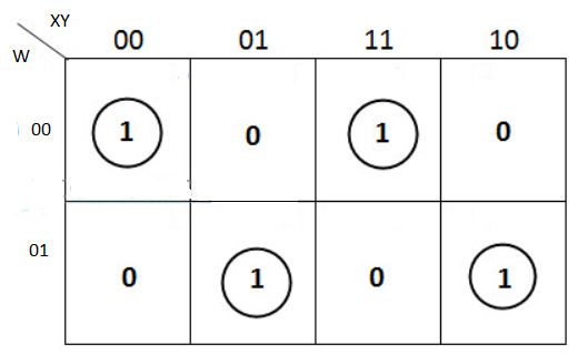

Parity Checker
- They are of two types:
- Even parity checker: It checks error in the transmitted data, which contains message bits along with even parity.
- Odd parity checker: It checks error in the transmitted data, which contains message bits along with odd parity.
Even parity checker
Assume a 3-bit binary input, W, X and Y is transmitted along with an even parity bit, P. So, the resultant data contains 4 bits, that is received as the input of even parity checker.
It generates an even parity bit, E. This bit is zero, if the received data contains an even number of ones, which indicates that there is no error in the received data and vice versa.
The Truth table of an even parity checker is:
4-bit Received Data WXYP | Even Parity Check bit E |
0000 | 0 |
0001 | 1 |
0010 | 1 |
0011 | 0 |
0100 | 1 |
0101 | 0 |
0110 | 0 |
0111 | 1 |
1000 | 1 |
1001 | 0 |
1010 | 0 |
1011 | 1 |
1100 | 0 |
1101 | 1 |
1110 | 1 |
1111 | 0 |
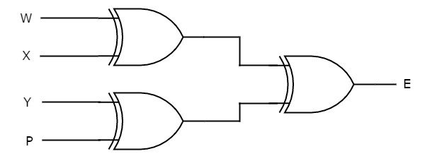
The Boolean function of even parity check bit as
E = W xor X xor Y xor P
The following figure shows the circuit diagram of even parity checker.
Odd Parity Checker
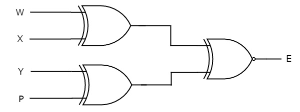
Assume a 3-bit binary input, W, X and Y is transmitted along with an odd parity bit, P. So, the resultant data contains 4 bits, that is received as the input of odd parity checker.
It generates an odd parity bit, E. This bit is zero, if the received data contains an odd number of ones, which indicates there is no error in the received data.
Key Takeaways:
- Even parity checker: It checks error in the transmitted data, which contains message bits along with even parity.
- Odd parity checker: It checks error in the transmitted data, which contains message bits along with odd parity.
- Even parity generator: It is generated in the transmitter end in message bits which contains even parity.
- Odd parity generator: It is generated in the transmitter end in message bits which contains odd parity.
- It is a special type of combinational circuit.
- It has n-data inputs, one output and m inputs select lines with 2m = n.
- It selects one of the n data inputs and routes it to the output.
- The selection of one of the inputs is done by the select lines.
- Depending on the code applied at the inputs, one of the n data sources is selected and transmitted to the single output Y.
- E is the enable input which is useful for cascading purpose.
- It is an active low terminal hence performs the required operation when it is low.
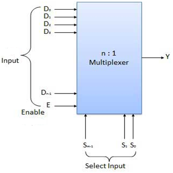
Fig. Block diagram of multiplexer
Multiplexers come in multiple variations
- 2: 1 multiplexer
- 4: 1 multiplexer
- 16: 1 multiplexer
- 32: 1 multiplexer
Block Diagram of 2:1 MUX
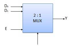
Truth Table of 2:1 MUX
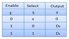
Where x is don’t care.
Key Takeaways
- It has n-data inputs, one output and m inputs select lines with 2m = n.
- The selection of one of the inputs is done by the select lines.
A Tree MUX connects a common to a set of output (or input) connections using SPDT relays. The signal is switched using a tree structure to expand the number of output connections supported. Since the relay is used to select which of two paths is closed the MUX only permits one overall path to be selected, and there is no possibility of unintentionally connecting output connections together.
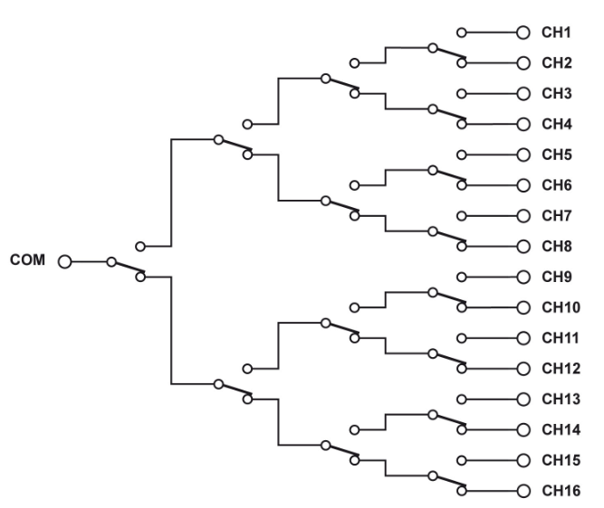
The path uses a number of relays in series so DC resistance of the thru path is higher than in a conventional MUX.
The number of relays required in the MUX is higher than a conventional MUX. Unless additional relays are added Tree MUX's always have a default path between the common and one output.
However, the MUX BW is considerably higher since the paths do not have open circuit traces or other relays connected to them that create transmission line stubs, so they have the best possible BW that the relays can provide.
Tree MUX's are often used as part of RF matrices in order to provide wide RF BW Tree and Crosspoint Matrices, at no point are there excess tracks connected to the RF path which minimises excess capacitive. A second use is in power systems where the input is to only be connected to one output, even in the event of a relay weld. As the MUX is created from changeover switches a welded relay inherently prevents an additional path from being connected.
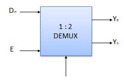
- It performs the inverse operation of a multiplexer as it receives one input and distributes it across its outputs.
- It has only one input and n outputs with m select input.
- At a time only one output line is selected by the select lines and that input is transmitted through the output line.
- It is equivalent to a single pole multiple way switch.
Various Demultiplexers are used as:
- 1: 2 demultiplexer
- 1: 4 demultiplexer
- 1: 16 demultiplexer
- 1: 32 demultiplexer
Block diagram
Truth Table
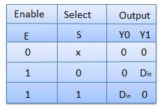
Where x is don’t care.
Key Takeaways:
- It performs the inverse operation of a multiplexer as it receives one input and distributes it across its outputs.
- It has only one input and n outputs with m select input.
Encoders
- It is a combinational circuit that converts binary information in the form of a 2N input lines into N output lines, which represent N bit code for the input.
- For simple encoders, only one input line is active at a time.
- For example: Octal to Binary encoder takes 8 input lines and generates 3 output lines.
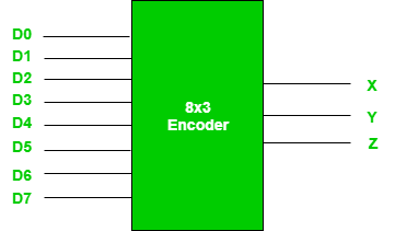
Fig. 8X3 Encoder
Truth Table –
D7 | D6 | D5 | D4 | D3 | D2 | D1 | D0 | X | Y | Z |
0 | 0 | 0 | 0 | 0 | 0 | 0 | 1 | 0 | 0 | 0 |
0 | 0 | 0 | 0 | 0 | 0 | 1 | 0 | 0 | 0 | 1 |
0 | 0 | 0 | 0 | 0 | 1 | 0 | 0 | 0 | 1 | 0 |
0 | 0 | 0 | 0 | 1 | 0 | 0 | 0 | 0 | 1 | 1 |
0 | 0 | 0 | 1 | 0 | 0 | 0 | 0 | 1 | 0 | 0 |
0 | 0 | 1 | 0 | 0 | 0 | 0 | 0 | 1 | 0 | 1 |
0 | 1 | 0 | 0 | 0 | 0 | 0 | 0 | 1 | 1 | 0 |
1 | 0 | 0 | 0 | 0 | 0 | 0 | 0 | 1 | 1 | 1 |
- From the above truth table it is seen that the output is 000 when D0 is active; 001 when D1 is active; 010 when D2 is active and so on.
Implementation –
- From the above truth table, the output Z is active when the input octal digit is 1, 3, 5 or 7.
- Y is active when input octal digit is 2, 3, 6 or 7 and X is active when input octal digits 4, 5, 6 or 7.
- Hence, the Boolean functions would be:
X = D4 + D5 + D6 + D7
Y = D2 +D3 + D6 + D7
Z = D1 + D3 + D5 + D7
- Hence, the encoder is realised with OR gates as follows:
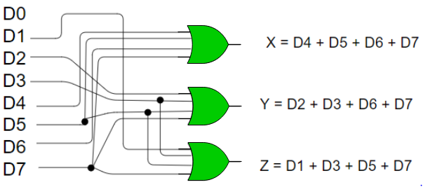
Fig: 8:3 encoder
- Limitation of the encoder is that only one input is active at a time.
- If more than one input are active, then the output of encoder is undefined.
- For example, if D6 and D3 are both active, then, our output would be 111 which is the output for D7.
- Problem arises when all inputs are 0.
- The encoder gives output 000 which actually is the output for D0. To avoid this, an extra bit is added to the output which is called the valid bit whose value is 0 when all inputs are 0 or 1.
Key Takeaways:
- It is a combinational circuit that converts binary information in the form of a 2N input lines into N output lines, which represent N bit code for the input.
- For simple encoders, only one input line is active at a time.
Decoders
- It works as an inverse of an encoder.
- It is a combinational circuit which converts n input lines into 2n output lines.
- Taking an example of 3-to-8 line decoder.
Truth Table –
X | Y | Z | D0 | D1 | D2 | D3 | D4 | D5 | D6 | D7 |
0 | 0 | 0 | 1 | 0 | 0 | 0 | 0 | 0 | 0 | 0 |
0 | 0 | 1 | 0 | 1 | 0 | 0 | 0 | 0 | 0 | 0 |
0 | 1 | 0 | 0 | 0 | 1 | 0 | 0 | 0 | 0 | 0 |
0 | 1 | 1 | 0 | 0 | 0 | 1 | 0 | 0 | 0 | 0 |
1 | 0 | 0 | 0 | 0 | 0 | 0 | 1 | 0 | 0 | 0 |
1 | 0 | 1 | 0 | 0 | 0 | 0 | 0 | 1 | 0 | 0 |
1 | 1 | 0 | 0 | 0 | 0 | 0 | 0 | 0 | 1 | 0 |
1 | 1 | 1 | 0 | 0 | 0 | 0 | 0 | 0 | 0 | 1 |
Implementation
D0 is high when X = 0, Y = 0 and Z = 0. Hence,
D0 = X’ Y’ Z’
Similarly,
D1 = X’ Y’ Z
D2 = X’ Y Z’
D3 = X’ Y Z
D4 = X Y’ Z’
D5 = X Y’ Z
D6 = X Y Z’
D7 = X Y Z
Hence,
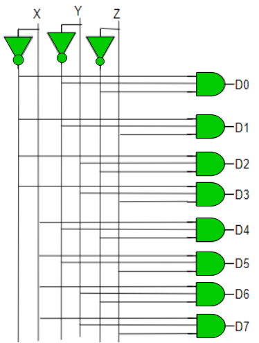
Fig. Decoder
Key Takeaways:
- It works as an inverse of an encoder.
- It is a combinational circuit which converts n input lines into 2n output lines.
In most practical applications, seven segment displays are used to give a visual indication of the output states of digital IC’s such a decade counters, latches etc. For using this display device, the data has to be converted from some binary code to the code required for the display. Usually, the binary code used is natural BCD.
The following figure shows the display device and the segments which must be illuminated for each of the numerals.

The display system can be connected as follows:
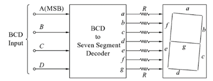
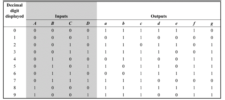
Here, ABCD is the natural BCD code for numerals 0 through 9. Following is the truth table of BCD to 7-segment decoder
The K-Maps for each of the outputs A through G are given below:
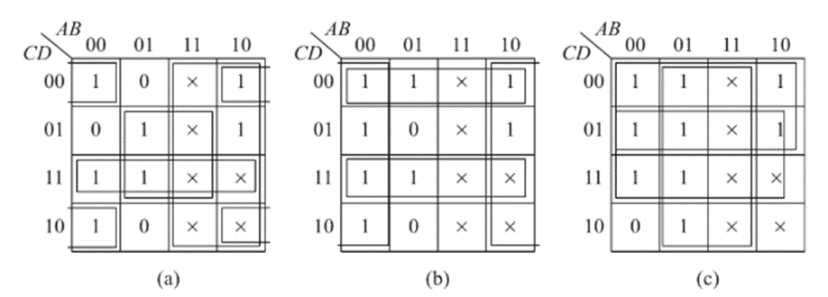
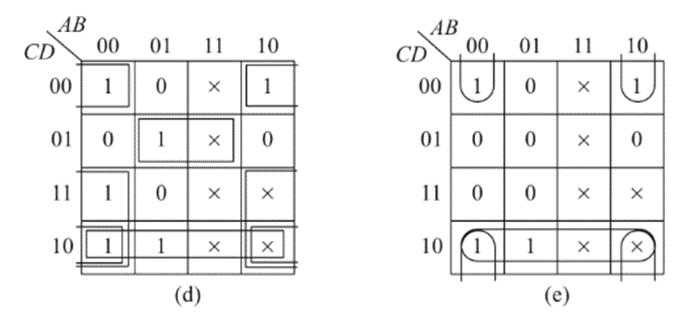
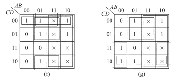
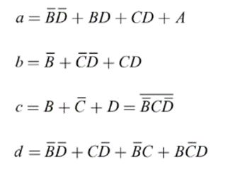
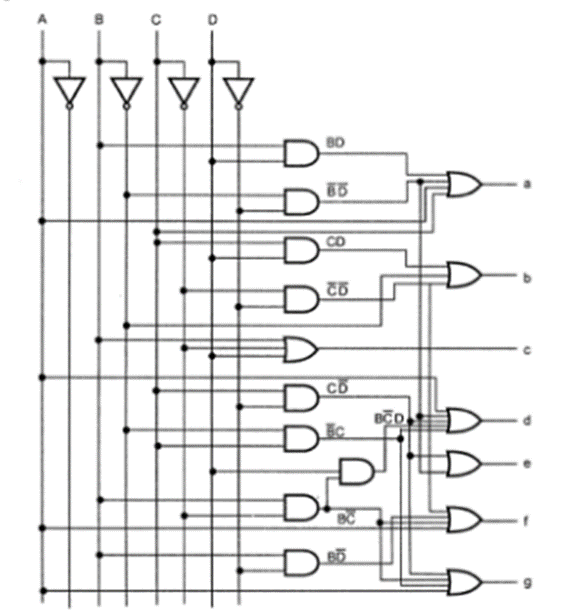
The simplified expressions obtained from the k-maps are:

Logic diagram:
Binary To Gray Code
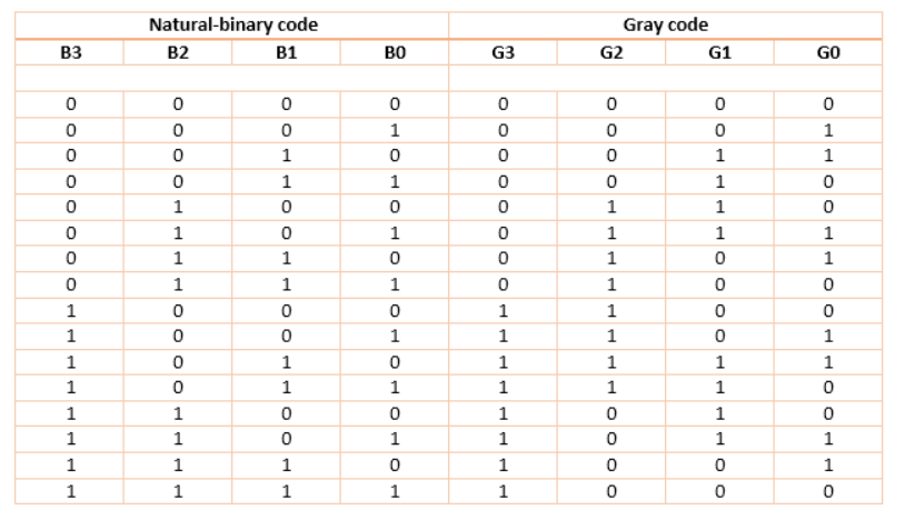
For this circuit, B3 B2 B1 B0 are inputs while G3 G2 G1 G0 are outputs.
K-map for the outputs:
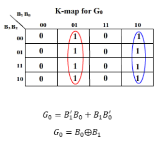
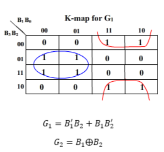
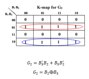
And G3 = B3
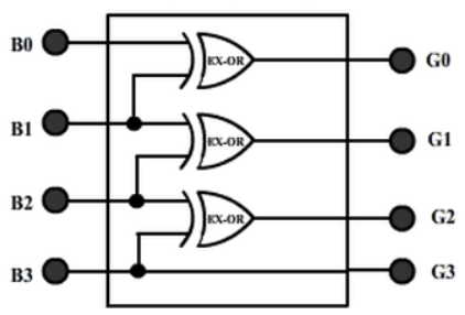
2. Gray To Binary Code
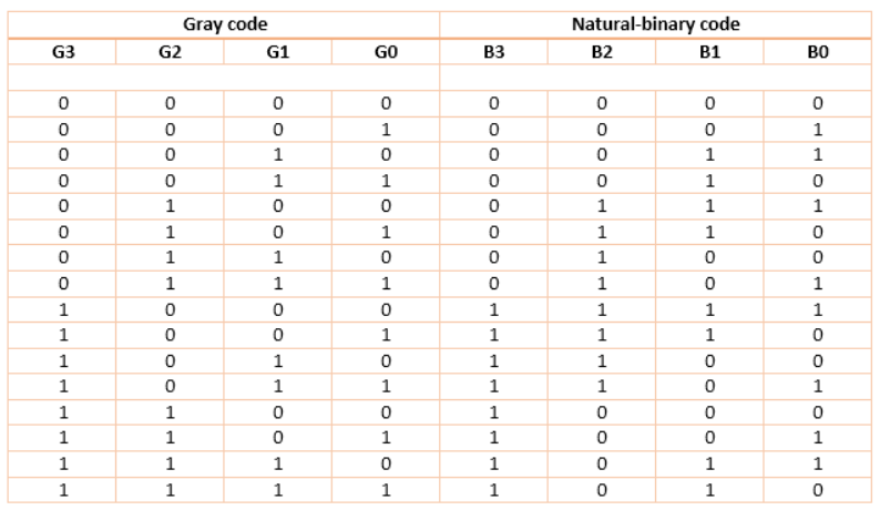
Then the K-maps:
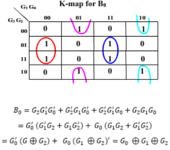
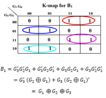
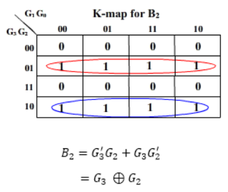
And B3 = G3
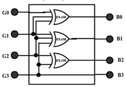
The realization of Gray-to-Binary converter is
Key Takeaways:
- These are the combinational circuits made by conversion of one code to another.
References:
1. Wakerly Pearon: “Digital Design: Principles and Practices”, Pearon Education Publications.
2. Mark Bach: “Complete Digital Design”, Tata MCGraw Hill Publications.
3. W. Fletcher: “Engg. Approach to Digital Design”, PHI Publications.