Unit - 3
Sequential Logic Design
A latch is a simple digital circuit where the output can be set to either logic 1 or logic 0 by an input signal. The circuit then remains in this state even after the input is removed. This is a memory circuit that can “remember” a single binary digit (bit).
SR Latch is a circuit which has:
(i) 2 cross-coupled NOR gate or NAND gate.
(ii) 2 input S for SET and R for RESET.
(iii) 2 output Q and Q’.
Q | Q’ | STATE |
1 | 0 | Set |
0 | 1 | Reset |
Under normal conditions, both the input remains 0.
RS Latch with NAND gates:
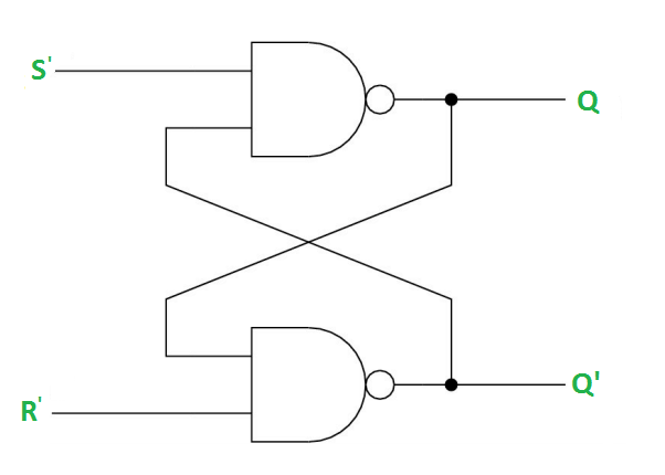
Case-1: When S’=R’=1 or S=R=0 then
If Q = 1, Q = R’ = 1.
If Q = 0, Q = 0 and R’ = 1 respectively.
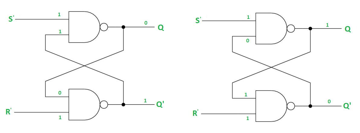
Case-2: S’=0, R’=1 (S=1, R=0)
As S’=0, Q = 1(SET state).
In 2nd NAND gate, as Q = R’ = 1, Q’=0.
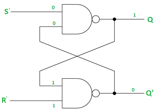
Case-3: S’= 1, R’= 0 (S=0, R=1)
As R’=0, Q’ = 1.
In 1st NAND gate, as Q =S’ = 1, Q=0 (RESET state).
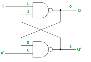
Case-4: S’= R’= 0 (S=R=1)
When S=R=1, both Q = Q’ = 1 which is not allowed.
So, this input condition is prohibited.
The SR Latch using NOR gate is:
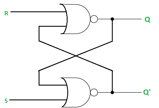
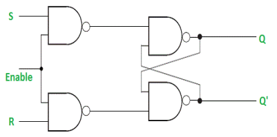
Gated SR Latch –
It is a latch which enable input that works when enable = 1 and retain the previous state when enable = 0.
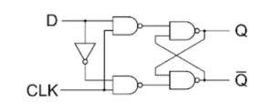
Gated D Latch –
It is similar to SR latch with little modifications. Here, the inputs are complements of one another. The design of D latch with Enable signal is given below:

The truth table is shown below:
ENABLE | D | Q(N) | Q(N+1) | STATE |
1 | 0 | x | 0 | RESET |
1 | 1 | x | 1 | SET |
0 | x | x | Q(n) | No Change |
As the output is same as input, it is also known as Transparent Latch.
The characteristic equation for D latch with enable input is given as:
Q(n+1) = EN.D + EN'.Q(n)
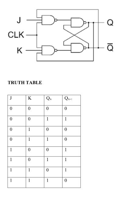
J-K Flip Flop:
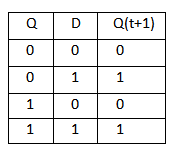
D Flip Flop
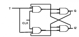
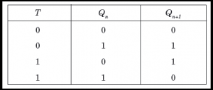
T Flip Flop
Conversion for Flip Flops
EXCITATION TABLE:
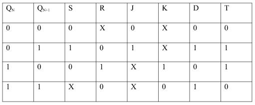
i) SR To JK Flip Flop
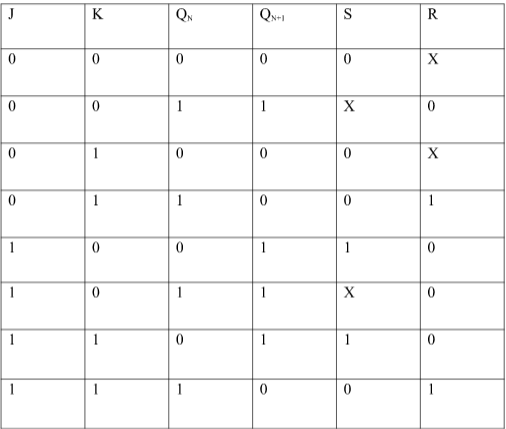
Excitation Functions:
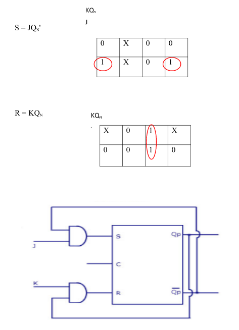
Ii) Convert SR To D Flip Flop:
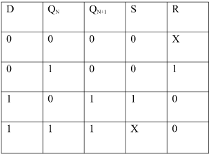
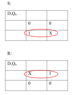
Excitation Functions:
S = D
R = D‘
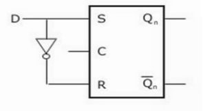
Master slave JK flip flop
Race Around Condition in JK Flip-flop –
- For J-K flip-flop, if J=K=1, and if clk=1 for a long period of time, then output Q will toggle as long as CLK remains high which makes the output unstable or uncertain.
- This problem is known as race around condition in J-K flip-flop.
- This problem can be avoided by ensuring that the clock input is at logic “1” only for a very short time.
- Hence the concept of Master Slave JK flip flop was introduced.
Master Slave JK flip flop –
It is basically a combination of two JK flip-flops connected together in series.
The first is the “master” and the other is a “slave”.
The output from the master is connected to the two inputs of the slave whose output is fed back to inputs of the master.
In addition to these two flip-flops, the circuit comprises of an inverter.
The inverter is connected to clock pulse in such a way that an inverted clock pulse is given to the slave flip-flop.
In other words, if CP=0 for a master flip-flop, then CP=1 for a slave flip-flop and vice versa.
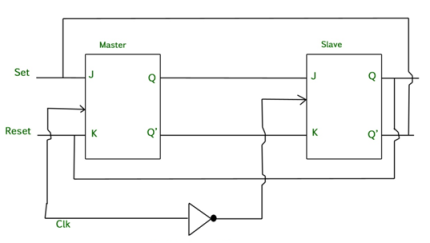
Fig. Master Slave Flip flop
Working of a master slave flip flop –
- When the clock pulse goes high, the slave is isolated; J and K inputs can affect the state of the system. The slave flip-flop is isolated when the CP goes low. When the CP goes back to 0, information is transmitted from the master flip-flop to the slave flip-flop and output is obtained.
- The master flip flop is positive level triggered and the slave flip flop is negative level triggered, hence the master responds prior to the slave.
- If J=0 and K=1, Q’ = 1 then the master goes to the K input of the slave and the clock forces the slave to reset therefore the slave copies the master.
- If J=1 and K=0, Q = 1 then the master goes to the J input of the slave and the Negative transition of the clock sets the slave and thus copy the master.
- If J=1 and K=1, the master toggles on the positive transition and the slave toggles on the negative transition of the clock.
- If J=0 and K=0, the flip flop becomes disabled and Q remains unchanged.
Timing Diagram of a Master flip flop –
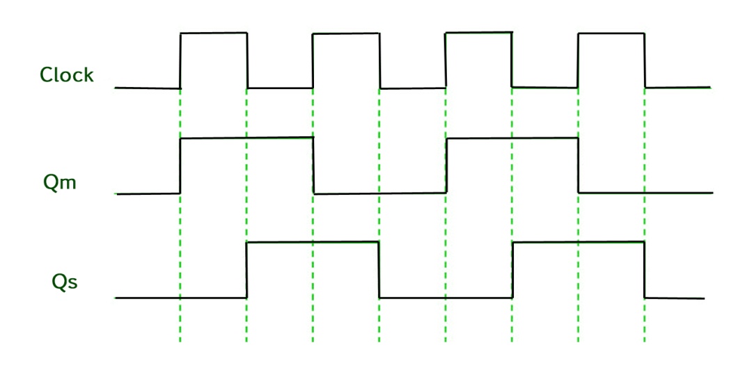
- When the CP = 1 then the output of master is high and remains high till CP = 0 because the state is stored.
- Now the output of master becomes low when the clock CP = 1 and remains low until the clock becomes high again.
- Thus toggling takes place for a clock cycle.
- When the CP = 1 then the master is operational but not the slave.
- When the clock is low, the slave becomes operational and remains high until the clock again becomes low.
- Toggling takes place during the whole process since the output changes once in a cycle.
- This makes the Master-Slave J-K flip flop a Synchronous device which passes data with the clock signal.
3.4 Use of preset and clear Terminals
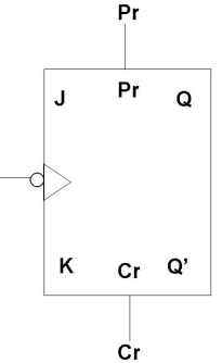
As flip flop may come up in random states when power is switched on, it is necessary to use some method where all the flip flops can be set or reset at the same time by a single switch – it is inconvenient to set or reset each flip flop individually. This is achieved by incorporating PRESET and CLEAR inputs in flip flops which can over-write all other inputs. These I/Ps are asynchronous and independent of the clock. While they are present, all other operations are inhibited. They force the output to a certain state irrespective of the I/Ps and clock.
Active High
Active High means that Preset and Clear I/Ps are inactive when low.
Pr = 1, Q = 1, Q’ = 0
i.e. if the Preset I/P is 1, the output will be forced to SET state irrespective of other I/Ps.
Cr = 1, Q = 0, Q’ = 1
i.e. if the Clear I/P is 1, the output will be forced to RESET state irrespective of other I/Ps.
It is not possible to Preset and Clear a flip flop at the same instant of time as Q can’t be 0 and 1 at the same time.
i.e. Pr = Cr ≠ 1 at any instant.
A register is a set of flip-flops with combinational logic to implement state transitions that allow information to be stored and retrieved from them. In the simplest form, a flip-flop is a one-bit register.
- Flip flops are used to store one bit of binary data (1or 0).
- If we need to store multiple bits of data, we use multiple flip flops.
- N flip flops are connected to store n bits of data.
- A Register is a device which stores such information. It is a group of flip flops connected in series which is used to store multiple bits of data.
- The information stored in these registers can be transferred with the help of shift registers.
- This register is a group of flip flops used to store multiple bits of data.
- The bits stored in these registers can be moved in/out of the registers by applying clock pulses.
- The registers which shift the bits towards left are called “Shift left registers”.
The registers which shift the bits towards right are called “Shift right registers”.
Shift registers are of 4 types and they are:
- Serial In Serial Out register
- Serial In parallel Out register
- Parallel In Serial Out register
- Parallel In parallel Out register
Serial-In Serial-Out Shift Register (SISO) –
- It allows serial input i.e. one bit after another and produces a serial output is known as Serial-In Serial-Out shift register.
- Since it has one output, the data leaves the register one bit at a time in a serial pattern, hence known as Serial-In Serial-Out Shift Register.
- The logic circuit is given underneath.
- The circuit comprises four D flip-flops which are connected serially.
- All these flip-flops are synchronous.

Fig. SISO
Serial-In Parallel-Out shift Register (SIPO) –
- It allows serial input through a single data line and produces a parallel output.
- The logic circuit is given underneath.
- The circuit consists of four D flip-flops which are connected synchronously.
- The clear (CLR) signal is also connected to all the 4 flip flops to RESET them.
- The output of the first flip flop is sent to the input of the next and so on.
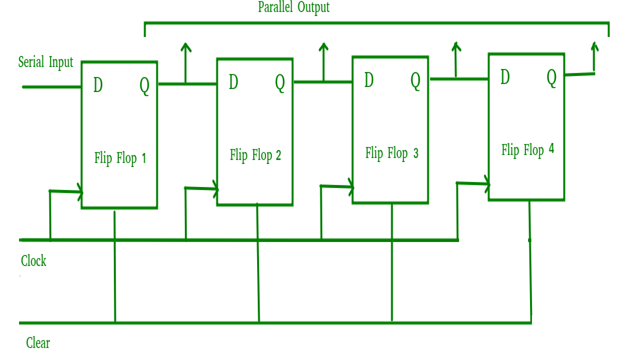
Fig. SIPO
- They are used in communication lines because the main use of the SIPO register is to convert serial data into parallel data.
Parallel-In Serial-Out Shift Register (PISO) –
- It allows parallel input data and produces a serial output.
- The logic circuit is given underneath.
- The circuit comprises four D flip-flops which are connected synchronously.
- The clock is connected to all the flip flops but the input data is connected to each flip flop individually through a multiplexer.
- The output of the previous flip flop and parallel data input are connected to the input of the MUX and the output of MUX is connected to the next flip flop.
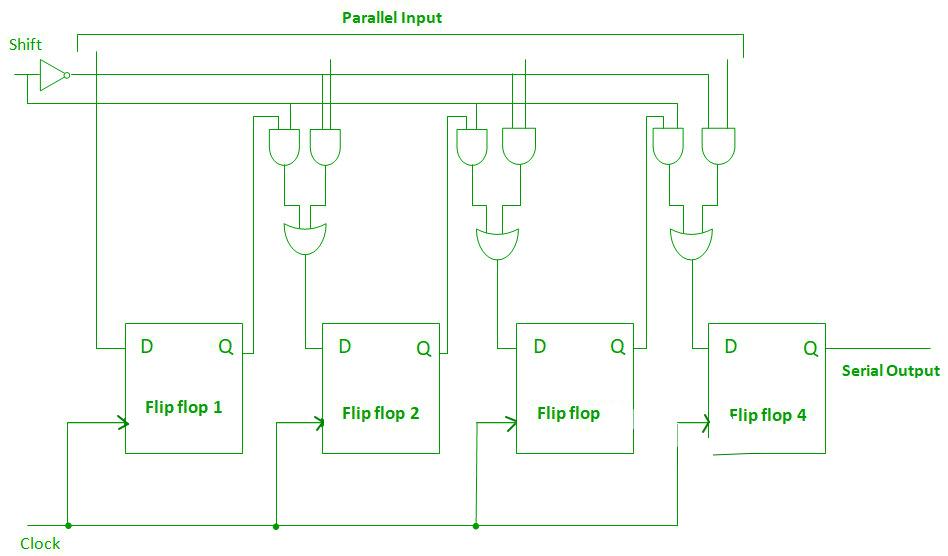
Fig. PISO
- It used to convert parallel data to serial data.
Parallel-In Parallel-Out Shift Register (PIPO) –
- It allows parallel input data and produces a parallel output.
- The logic circuit is given underneath.
- The circuit comprises four D flip-flops which are connected synchronously.
- The clear (CLR) and clock signals are connected to all flip flops.
- In this, there are no interconnections between flip-flops as no serial shifting of the data is required.
- Data is provided separately as input for each flip flop and the output is also collected individually from each flip flop.
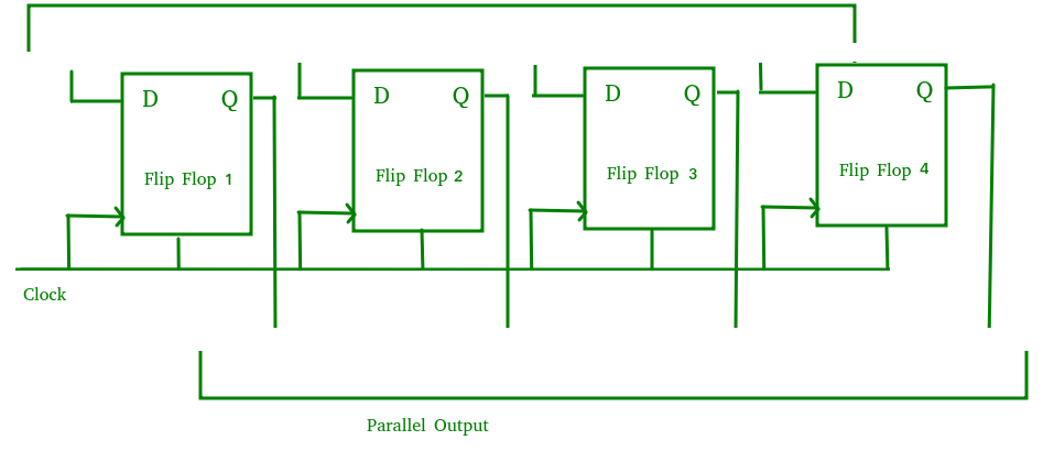
Fig. PIPO
- It is used as a temporary storage device and it acts as a delay element too.
Applications of Shift Registers
- They are used for temporary data storage.
- They are used for data transfer and data manipulation.
- The SISO and PIPO registers are used to produce time delay in digital circuits.
- The SIPO register is used for conversion of serial data to parallel data hence they are used in communication lines.
- A PISO register is used to convert parallel data to serial data.
References:
1. Wakerly Pearon: “Digital Design: Principles and Practices”, Pearon Education Publications.
2. Mark Bach: “Complete Digital Design”, Tata MCGraw Hill Publications.
3. W. Fletcher: “Engg. Approach to Digital Design”, PHI Publications.