Unit - 5
8085 Programming & Interrupts
- The 8008 processor was invented in the year 1972. The clock speed of this microprocessor is 500 kHz and instruction per second is 50K
- The 8080 microprocessor was invented in the year 1974. The clock speed is 2 MHz. The number of transistors used is 60k and instruction per second is 10 times quicker as compared with 8008 processor.
- The 8085 microprocessor was invented in the year 1976. The clock speed is 3 MHz. The number of transistors used is 6,500 and instruction per second is 769230. The number of pins of this microprocessor is 40
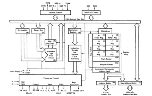
8085 consists of the following functional units −
Accumulator
The accumulator is an 8-bit register used to perform arithmetic, logical, I/O & LOAD/STORE operations. It is connected to internal data bus & ALU.
Arithmetic and logic unit
The arithmetic and logic unit performs arithmetic and logical operations like Addition, Subtraction, AND, OR, etc. on 8-bit data.
General purpose register
8085 consists of six general purpose registers in 8085 processor that is B, C, D, E, H & L. Each register holds 8-bit data. These registers work in pair to hold 16-bit data and their pairing combination is like B-C, D-E & H-L.
Program counter
It is a 16-bit register used to store the memory address location of the next instruction to be executed. Microprocessor increments the program whenever an instruction is being executed, so that the program counter points to the memory address of the next instruction that is going to be executed.
Stack pointer
It is 16-bit register which works like stack, which gets incremented/decremented by 2 during push & pop operations.
Temporary register
It is an 8-bit register, which holds the temporary data of arithmetic and logical operations.
Flag register
It is an 8-bit register which holds 0 or 1 depending upon the result stored in the accumulator.
These are:
- Sign (S)
- Zero (Z)
- Auxiliary Carry (AC)
- Parity (P)
- Carry (C)

Instruction registers and decoder
It is an 8-bit register. When an instruction is fetched from memory then it is stored in the Instruction register. Instruction decoder decodes the information present in the Instruction register.
Timing and control unit
It provides timing and control signal to the microprocessor to perform operations. Following are the timing and control signals, which control external and internal circuits −
- Control Signals: READY, RD’, WR’, ALE
- Status Signals: S0, S1, IO/M’
- DMA Signals: HOLD, HLDA
- RESET Signals: RESET IN, RESET OUT
Interrupt control
It controls the interrupts during the process. When the microprocessor is executing the main program and whenever an interrupt occurs, the microprocessor shifts the control from the main program to process the incoming request. After the request is completed, the control returns to the main program.
There are 5 interrupt signals in 8085 microprocessors:
- INTR
- RST 7.5
- RST 6.5
- RST 5.5
- TRAP.
Serial Input/output control
It controls the serial data communication by using the two instructions: SID (Serial input data) and SOD (Serial output data).
Address buffer and address-data buffer
The content stored in the stack pointer and program counter is loaded into the address buffer and address-data buffer to communicate with the CPU.
The memory and I/O chips are connected to these buses, the CPU can exchange the desired data with the memory and I/O chips.
Address bus and data bus
Data bus carries the data to be stored. It is bidirectional whereas address bus carries the location to where it should be stored, and it is unidirectional. It is used to transfer the data & Address I/O devices.
- Address bus A15-A8.
- Data bus AD7-AD0.
- Three control signals are RD, WR & ALE.
- RD: It indicates that the selected IO or memory device can be read and is ready to accept data available on the data bus.
- WR: It indicates that the data on the data bus can be written into a selected memory or IO location.
- ALE: It is a positive going pulse that is generated when a new operation is started by the microprocessor. When high, it indicates address and when low, it indicates data.
- Three status signals are IO/M, S0 & S1.
- IO/
 : It is used for input/output or memory selection i.e. when it is high it indicates IO operation and when it is low then it indicates memory operation.
 - S1 & S0: They are used to identify the type of current operation.
- Power supply: VCC & VSS.
- VCC: +5V and VSS : ground signal (0V).
- Clock signals: There are 3 types of clock signals, X1, X2 and CLK OUT.
- X1, X2: A crystal (RC, LC N/W) is connected at these two pins and is used to set frequency of the internal clock generator. This frequency is internally divided by 2.
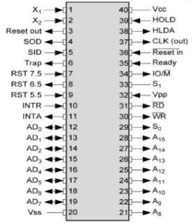
Fig: Pin diagram of 8085
- CLK OUT: This signal is used as the system clock for devices connected with the microprocessor.
- Interrupts are the signals generated by external devices requesting the microprocessor to perform a certain task. There are 5 types of interrupt. They are TRAP, RST 7.5, RST 6.5, RST 5.5, and INTR.
- INTA: It is an interrupt acknowledge signal.
- RESET IN: It is used to reset the microprocessor by setting the program counter to zero.
- RESET OUT: It is used to reset all the devices connected to the microprocessor when microprocessor is reset.
- READY: It indicates that the device is ready to send or receive data. If it is low, then the CPU has to wait for it to go high.
- HOLD: It indicates that another master is requesting the use of the address and data buses.
- HLDA: It stands for HOLD Acknowledge. It indicates that the CPU has received the HOLD request and is ready to share the bus in the next clock cycle. After the HOLD signal is removed HLDA is set to low.
- SID and SOD signals are used for serial communication.
- SOD (Serial output data line): It is set/reset by the SIM instruction.
- SID (Serial input data line): when it is active, the data on this line is loaded into accumulator whenever a RIM instruction is executed.
Interrupt is signals send by an external device to the processor, to request the processor to perform a particular task Mainly in the microprocessor based system the interrupts are used for data transfer between the peripheral and the microprocessor.
The processor will check the interrupts always at the 2nd T-state of last machine cycle.
If there is any interrupt it will accept the interrupt and send the INTA (active low) signal to the peripheral.
The vectored address of interrupt is stored in program counter.
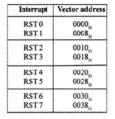
The processor executes an interrupt service routine (ISR) addressed in program counter. It returned to main program by RET instruction.
Types of Interrupts: It supports two types of interrupts.
1. Hardware interrupts
2. Software interrupts
Software interrupts: The software interrupts are program instructions. These instructions are inserted at desired locations in a program. The 8085 has eight software interrupts from RST 0 to RST 7. The vector address for these interrupts can be calculated as follows. The Table shows the vector addresses of all interrupts.
Hardware interrupts: An external device initiates the hardware interrupts and placing an appropriate signal at the interrupt pin of the processor. If the interrupt is accepted, then the processor executes an interrupt service routine.
Data Transfer Instruction
These instructions transfer data between registers or between memory and registers. The instruction is used to copy data from source to destination while copying the contents of source cannot be modified.

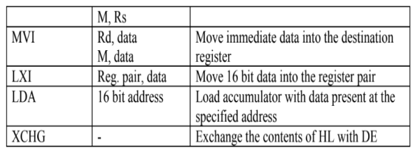
For example MOV B,C
MVI B,20H
LXI H, 4020H
LDA 6000H
Arithmetic Instructions
- Addition
- Subtraction
- Increment
- Decrement
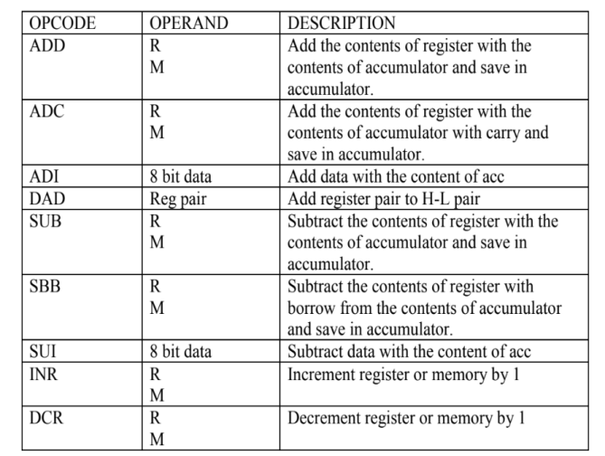
For example:
ADD C
ADC M
ADI 40H
DAD HL
SUB B
SUI 20H
INR C
Logical Instructions
The logical operations are:
- AND
- OR
- XOR
- Rotate
- Compare
- Complement
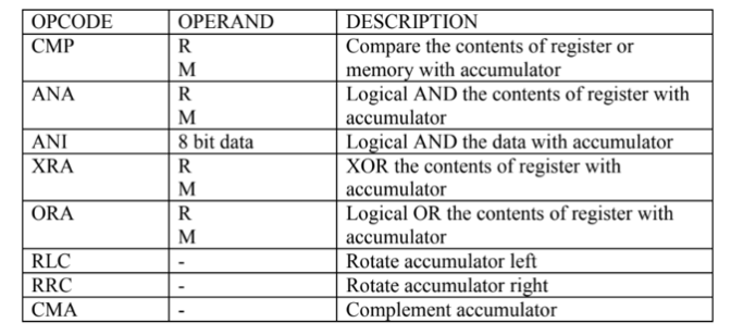
For example
CMP C
ANA B
ANI 40H
XRA M
ORA C
RLC
Branching Instructions
These instructions alter the normal sequential flow conditionally or unconditionally
OPCODE | OPERAND | DESCRIPTION |
JMP | 16-bit address | Jump unconditionally to the given location |
JC | 16-bit address | Jump if carry |
JNC | 16-bit address | Jump if no carry |
JZ | 16-bit address | Jump if zero |
JNZ | 16-bit address | Jump if no zero |
CALL | 16-bit address | Call unconditionaly |
RET | 16-bit address | Return unconditionally |
RST | 16-bit address | Restart (Software Interrupts) |
For example
JMP 2000H
RET
RST 6
Control Instructions
It controls the operation of microprocessor

For example
NOP
EI
SIM
Machine language and Hex code instructions are difficult for the programmer. Hence for programmer, the instructions of microprocessor are made in the form of English abbreviation (short form).
These instructions are name as Assembly Language instructions or mnemonics. The combinations of different mnemonics are known as Assembly Language Program and it is a low- level language.
Write a program to transfer 07 H in register L
Memory address | Machine Code | Mnemonics | Operands | Comments |
2000H | 2E,07 | MVI | L,07 | Move immediate 07 in register L |
2002H | 76 | HLT |
| Stop or terminate the program |
The instruction MVI L, 07 will move the data 07 to the register L. The instruction will stop the program. The machine code for the instruction MVI L, 07 is 2E, 07. The 1st byte of the machine code is 2E which is the Hex code for the instruction MVI L. The second byte is the data 07.
The machine code for HLT is 76.
The machine codes are fetch in the memory locations, starting from the memory locations 2000 H. Memory location 2000 H contains 2E, 2001 H contains 07 and memory location 2002 H contain 76.
After the execution of a program, the contents of Register L can be examined which are 07.
The 8085 has five hardware interrupts
(1) TRAP
(2) RST 7.5
(3) RST 6.5
(4) RST 5.5
(5) INTR
TRAP: This interrupt is a non-maskable interrupt. It is unaffected by any mask or interrupt enable. TRAP has the highest priority and vectored interrupt. TRAP interrupt is edge and level triggered. This means hat the TRAP must go high and remain high until it is acknowledged. In sudden power failure, it executes a ISR and send the data from main memory to backup memory. The signal, which overrides the TRAP, is HOLD signal. (i.e., If the processor receives HOLD and TRAP at the same time then HOLD is recognized first and then TRAP is recognized).
There are two ways to clear TRAP interrupt.
1. By resetting microprocessor (External signal)
2. By giving a high TRAP ACKNOWLEDGE (Internal signal)
RST 7.5: The RST 7.5 interrupt is a maskable interrupt. It has the second highest priority. It is edge sensitive. Ie. Input goes to high and no need to maintain high state until it recognized. Maskable interrupt. It is disabled by,
1. DI instruction
2. System or processor reset.
3. After reorganization of interrupt.
Enabled by EI instruction.
RST 6.5 and 5.5: The RST 6.5 and RST 5.5 both are level triggered. Ie. Inputs goes to high and stay high until it recognized.
Maskable interrupt. It is disabled by,
1.DI, SIM instruction
2.System or processor reset.
3. After reorganization of interrupt. Enabled by EI instruction. The RST 6.5 has the third priority whereas RST 5.5 has the fourth priority.
INTR: INTR is a maskable interrupt. It is disabled by,
1.DI, SIM instruction
2.System or processor reset.
3.After reorganization of interrupt.
Enabled by EI instruction. Non- vectored interrupt. After receiving INTA (active low) signal, it has to supply the address of ISR. It has lowest priority. It is a level sensitive interrupts. Ie. Input goes to high and it is necessary to maintain high state until it recognized.
The following sequence of events occurs when INTR signal goes high.
1. The 8085 checks the status of INTR signal during execution of each instruction.
2. If INTR signal is high, then 8085 complete its current instruction and sends active low interrupt acknowledge signal, if the interrupt is enabled.
3. In response to the acknowledge signal, external logic places an instruction OPCODE on the data bus. In the case of multibyte instruction, additional interrupt acknowledge machine cycles are generated by the 8085 to transfer the additional bytes into the microprocessor.
4. On receiving the instruction, the 8085 save the address of next instruction on stack and execute received instruction.
References:
1. Wakerly Pearon: “Digital Design: Principles and Practices”, Pearon Education Publications.
2. Mark Bach: “Complete Digital Design”, Tata MCGraw Hill Publications.
3. W. Fletcher: “Engg. Approach to Digital Design”, PHI Publications.