Unit - 3
Digital Communication
Sampling is defined as, “The process of measuring the instantaneous values of continuous-time signal in a discrete form.”
Sample is a piece of data taken from the whole data which is continuous in the time domain.
When a source generates an analog signal and if that has to be digitized, having 1s and 0s i.e., High or Low, the signal has to be discretized in time. This discretization of analog signal is called as Sampling.
The following figure indicates a continuous-time signal x (t) and a sampled signal xs (t). When x (t) is multiplied by a periodic impulse train, the sampled signal xs (t) is obtained.
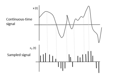
Fig 1. Sampled Signal
Sampling Rate
To discretize the signals, the gap between the samples should be fixed. That gap can be termed as a sampling period Ts.
Sampling Frequency=1/Ts=fs
Where,
- Ts is the sampling time
- Fs is the sampling frequency or the sampling rate
Sampling frequency is the reciprocal of the sampling period. This sampling frequency, can be simply called as Sampling rate. The sampling rate denotes the number of samples taken per second, or for a finite set of values.
Nyquist Rate
Suppose that a signal is band-limited with no frequency components higher than W Hertz. That means, W is the highest frequency. For such a signal, for effective reproduction of the original signal, the sampling rate should be twice the highest frequency.
Which means,
FS=2W
Where,
- FS is the sampling rate
- W is the highest frequency
This rate of sampling is called as Nyquist rate.
Examples:
1) The continuous-time signal x(t) = cos(200πt) is used as the input for a CD converter with the sampling period 1/300 sec. Determine the resultant discrete-time signal x[n].
Solution:
We know,
X[n] =x(nT)
= cos(200πnT)
= cos(2πn/3) , where n= -1,0,1,2……
The frequency in x(t) is 200π rad/s while that of x[n] is 2π/3.
2) Determine the Nyquist frequency and Nyquist rate for the continuous-time signal x(t) which has the form of:
X(t) = 1+ sin(2000πt) + cos (4000πt)
Solution:
The frequencies are 0, 2000π and 4000π.
The Nyquist frequency is 4000π rad/s and the Nyquist rate is 8000π rad/s.
3) Consider an analog signal 
Find the Nyquist rate?
Solution
The frequency in the analog signal

The largest frequency is

The Nyquist rate is

4) The analog signal 
- What is the Nyquist rate for this signal?
- Using a sampling rate
 . What is discrete time signal obtained after sampling?
 - What is analog signal
 we can reconstruct from the samples if we use ideal interpolation?
Solution.
- The frequency of the analog signal are


- For


For  ,the folding frequency is
Hence  is not effected by aliasing
 Is changed by the aliasing effect
 Is changed by the aliasing effect
So that normalizing frequencies are

The analog signal that we can recover is

Which is different than the original signal 
5) For 
- Find the minimum sampling rate required to avoid aliasing.
- If
 , what is the discrete time signal after sampling?
 - If
 , what is the discrete time signal after sampling?
 - What is the frequency F of a sinusoidal that yields sampling identical to obtained in part c?
Solution. a. 
The minimum sampling rate is

And the discrete time signal is

b. If  , the discrete time signal is

c. If Fs=75Hz , the discrete time signal is

d. For the sampling rate 
 in part in (c). Hence

So, the analog sinusoidal signal is


6) Suppose a continuous-time signal x(t) = cos (Ø0t) is sampled at a sampling frequency of 1000Hz to produce x[n]: x[n] = cos(πn/4)
Determine 2 possible positive values of Ø0, say, Ø1 and Ø2. Discuss if cos(Ø1t) or cos(Ø2t) will be obtained when passing through the DC converter.
Solution:
Taking T= 1/1000s
Cos(πn/4) =x[n] = x(nT) = cos (Ø0n/1000)
Ø1 is easily computed as 
Ø1 = 250π
Ø2 can be obtained by noting the periodicity of a sinusoid:
 Ø2n/1000)
Ø2 = 2250π
The sampling theorem, which is also called as Nyquist theorem, delivers the theory of sufficient sample rate in terms of bandwidth for the class of functions that are bandlimited.
The sampling theorem states that, “a signal can be exactly reproduced if it is sampled at the rate fs which is greater than twice the maximum frequency W.”
Let us consider a band-limited signal, i.e., a signal whose value is non-zero between some –W and W Hertz.
Such a signal is represented as x(f)=0 for ∣f∣>W
For the continuous-time signal x (t), the band-limited signal in frequency domain, can be represented as shown in the following figure.
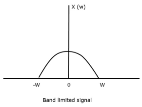
Fig 2. Band limited Signal
If the signal x(t) is sampled above the Nyquist rate, the original signal can be recovered, and if it is sampled below the Nyquist rate, the signal cannot be recovered.
The following figure explains a signal, if sampled at a higher rate than 2w in the frequency domain.
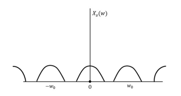
Fig 3. Fourier Transform of xs(t)
The above figure shows the Fourier transform of a signal xs (t).
If fs<2W
The resultant pattern will look like the following figure.
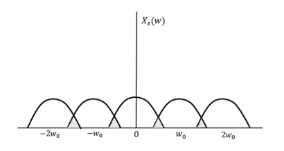
Fig 4. Output Waveform
Here, the over-lapping of information is done, which leads to mixing up and loss of information. This unwanted phenomenon of over-lapping is called as Aliasing.
Aliasing
Aliasing can be referred to as “the phenomenon of a high-frequency component in the spectrum of a signal, taking on the identity of a low-frequency component in the spectrum of its sampled version.”
Key Takeaways:
- If the signal x(t) is sampled above the Nyquist rate, the original signal can be recovered, and if it is sampled below the Nyquist rate, the signal cannot be recovered.
- The over-lapping of information is done, which leads to mixing up and loss of information. This unwanted phenomenon of over-lapping is called as Aliasing.
Ideal Sampling
Impulse sampling or ideal sampling can be performed by multiplying input signal x(t) with impulse train y(t) =  (t – nTs) of period T.
The amplitude of impulse changes with respect to amplitude of input signal x(t). The output of sampler is given by
y(t)=x(t)×y(t) ---------------------(1)
=x(t)× impulse train--------------------(2)
=x(t)×  (t – nTs) -------------------------(3)
y(t) = yδ(t) =  (t – nTs) --------------------------(4)
To get the spectrum of sampled signal, consider Fourier transform of equation (4) on both sides
Y(ω)= 1/Ts  ) ---------------------------------------(5)
This is called ideal sampling or impulse sampling.

Natural Sampling
Natural sampling is similar to impulse sampling, except the impulse train is replaced by pulse train of period T.
Multiplying x(t) by pulse train  )
)
The output of sampler is
y(t)=x(t)×pulse train
=x(t)×p(t) -----------------------------(1)
=x(t)×  -----------------------(2)
The exponential Fourier series representation of p(t) can be given as
p(t) =  n e jnwst -----------------------------(3)
=  n e j2πfst -------------------------------(4)
Where Fn = 1/T  e –jnwst dt --------------------------(5)
= 1/TP (nws)
Substitute Fn in equation(3)
p(t) =  P(nws) ejnwst ------------------------------------(6)
= 1/T  ) ejnwst -------------------------------------------(7)
y(t) = x(t) x p(t)
= x(t) x 1/T  ) ejnwst ------------------------------(8)
y(t) = x(t) x 1/T  ejnwst --------------------------(9)
y(t) = 1/T  x(t) ejnwst --------------------------------------(10)
Consider Fourier Transform on both sides
F.T [y(t)] = 1/T  F.T [x(t) ejnwst ] ------------------------------(11)
F.T [x(t) ejnwst ] = X(w – nws) -----------------------------(12)
Y(w) = 1/T  X(w – nws) ----------------------------------(13)
Natural sampling is similar to impulse sampling, except the impulse train is replaced by pulse train of period T.

Flat Top Sampling
During transmission, noise is introduced at top of the transmission pulse which can be easily removed if the pulse is in the form of flat top. Here, the top of the samples are flat i.e. they have constant amplitude. Hence, it is called as flat top sampling or practical sampling. Flat top sampling makes use of sample and hold circuit.

Fig 5. Flat top Sampled Signal

Fig 6. Flat top signal obtained after convolution
The sampled signal can be obtained by convolution of rectangular pulse p(t) with ideally sampled signal say yδ(t) as shown in the diagram above
y(t) = p(t) x yδ(t)
Taking F.T of above signal we get

From convolution


Key takeaway
- This is indeed a strategy with the least noise disturbance to that of the measured signal.
- This is accomplished by making the sequencing mechanism or feature multiplies the input message.
- This seems to be a convenient tool used to analyse signals.
Aliasing Effect
- When fs>2 fm due to aliasing there is loss of information as seen from the above figure. The signal components do not possess fm. Some components are outside the bandwidth.
- In order to avoid aliasing the anti-aliasing filters are used. The cut off frequency fs/2 of the filter needs to be higher than the bandwidth of the system.
- There is dead time in the system due to conversion of signals. Hence, the sampling interval is selected in such a manner that the stability limit of the closed loop control system as the sampling interval is increased.
- As the signal is converted to digital form errors occur. As the sampling interval increases the error also increase.
Aperture effect
- The amplitude of the flat top signal must be constant, but sometimes it is not constant due to the high frequency roll off of the sampling signal.
- This results in the attenuation in the high frequency part of the message spectrum.
- Thus, the sampled signal in the flat top sampling consists of attenuated high frequency components and this effect is known as Aperture effect.
- Aperture effect can be improved by selecting value of pulse width τ to be very small and by using equalizer circuit.
If the waveform is under sampled (when. Fs < 2B) then the signal at the output of the filter will be different from the original signal spectrum This results in aliasing.
This implies that whenever the sampling condition is not met, an irreversible overlap of the spectral replicas is produced then there will be spectral overlap in the sample.
PAM
In PAM, amplitude of pulses is varied in accordance with instantaneous value of modulating signal.
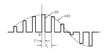
Fig 7. PAM waveform
PAM Generation:
The carrier which is in the form of narrow pulses has frequency fc. The uniform sampling takes place in multiplier to generate PAM signal. Samples are placed Ts sec away from each other.
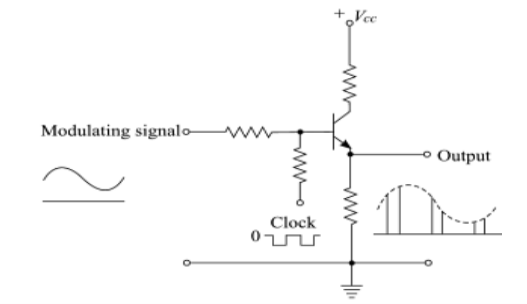
Fig 8. PAM Modulator
- The circuit is simple emitter follower.
- In the absence of the clock signal, the output follows input.
- The modulating signal is applied as the input signal.
- Another input to the base of the transistor is the clock signal.
- The frequency of the clock signal is made equal to the desired carrier pulse train frequency.
- The amplitude of the clock signal is chosen the high level is at ground level(0v)
- Low level at some negative voltage sufficient to bring the transistor in cutoff region.
- When clock is high, circuit operates as emitter follower and the output follows in the input modulating signal.
- When clock signal is low, transistor is cutoff and output is zero.
- Thus the output is the desired PAM signal.
PAM Demodulator:
The PAM demodulator circuit which is just an envelope detector followed by a second order op-amp low pass filter (to have good filtering characteristics) is as shown below
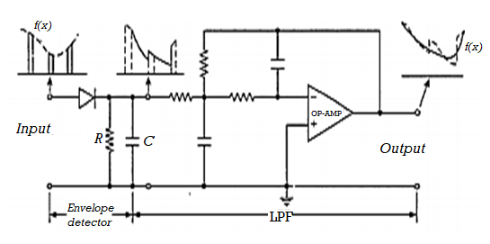
Fig 9. PAM Demodulator
Key takeaway
The carrier which is in the form of narrow pulses has frequency fc. The uniform sampling takes place in multiplier to generate PAM signal. Samples are placed Ts sec away from each other.
PWM and PPM
There are two types of PTM systems. They are Pulse width modulation (PWM) and Pulse Position Modulation (PPM).
Pulse Width Modulation
In this type of modulation, the amplitude is maintained constant but the width of each pulse is varied in accordance with instantaneous value of the analog signal. In PWM information is contained in width variation. This is similar to FM. In pulse width modulation (PWM), the width of each pulse is made directly proportional to the amplitude of the information signal.
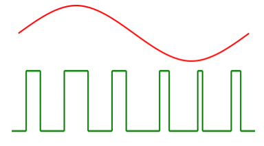
Fig 10. PWM waveform
PPM
In this type of modulation, the sampled waveform has fixed amplitude and width whereas the position of each pulse is varied as per instantaneous value of the analog signal. PPM signal is further modification of a PWM signal.
PPM and PWM modulator
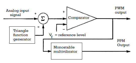
Fig 11. PTM Modulator
- The PPM signal can be generated from PWM signal.
- The PWM pulses obtained at the comparator output are applied to a mono stable multi vibrator which is negative edge triggered.
- Hence for each trailing edge of PWM signal, the monostable output goes high. It remains high for a fixed time decided by its RC components.
- Thus as the trailing edges of the PWM signal keeps shifting in proportion with the modulating signal, the PPM pulses also keep shifting.
- Therefore all the PPM pulses have the same amplitude and width. The information is conveyed via changing position of pulses.
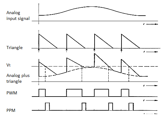
Fig 12. PWM and PPM Modulation waveforms.
PWM Demodulator
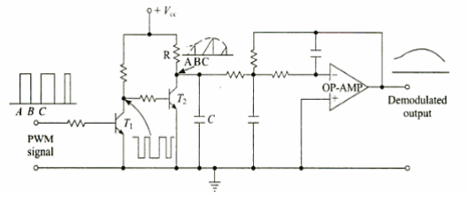
Fig 13. PWM Demodulator
- Transistor T1 works as an inverter.
- During time interval A-B when the PWM signal is high the input to transistor T2 is low.
- Therefore, during this time interval T2 is cut-off and capacitor C is charged through an R-C combination.
- During time interval B-C when PWM signal is low, the input to transistor T2 is high, and it gets saturated.
- The capacitor C discharges rapidly through T2.
- The collector voltage of T2 during BC is low.
- Thus, the waveform at the collector of T2is similar to saw-tooth waveform whose envelope is the modulating signal.
- Passing it through 2nd order op-amp Low Pass Filter, gives demodulated signal.
PPM Demodulator
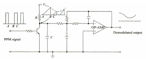
Fig 14. PPM Demodulator
- The gaps between the pulses of a PPM signal contain the information regarding the modulating signal.
- During gap A-B between the pulses the transistor is cut-off and the capacitor C gets charged through R-C combination.
- During the pulse duration B-C the capacitor discharges through transistor and the collector voltage becomes low.
- Thus, waveform across collector is saw-tooth waveform whose envelope is the modulating signal.
- Passing it through 2nd order op-amp Low Pass Filter, gives demodulated signal.
Key takeaway
In pulse time modulation system, we use the increased bandwidth consumed by pulses to obtain an improvement in noise performance by representing the sample values of the message signal by some property of pulse rather than amplitude.
Comparison between PAM, PPM and PWM
SR. NO. | PARAMETER | PAM | PWM | PPM |
1 | Type of Carrier | Train of Pulses | Train of Pulses | Train of Pulses |
2 | Variable Characteristic of the Pulsed Carrier | Amplitude | Width | Position |
3 | Bandwidth Requirement | Low | High | High |
4 | Noise Immunity | Low | High | High |
5 | Information Contained in | Amplitude Variations | Width Variations | Position Variations |
6 | Transmitted Power | Varies with amplitude of pulses | Varies with variation in width | Remains Constant |
7 | Need to transmit synchronizing pulses | Not needed | Not needed | Necessary |
8 | Complexity of generation and detection | Complex | Easy | Complex |
9 | Similarity with other Modulation Systems | Similar to AM | Similar to FM | Similar to PM |
10 | Output waveforms | Refer Figure down | Refer Figure down | Refer Figure down |
Basic Elements of PCM
The transmitter section comprises of Sampling, Quantizing and Encoding. The low pass filter prior to sampling prevents aliasing of the message signal.
The basic operations in the receiver section are regeneration of impaired signals, decoding, and reconstruction of the quantized pulse train.
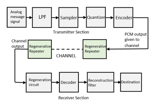
Fig 15: PCM
Low Pass Filter
This filter eliminates the high frequency components present in the input analog signal to avoid aliasing of the message signal.
Sampler
It helps to collect the sample data at instantaneous values of message signal, so as to reconstruct the original signal. The sampling rate must be in accordance with the sampling theorem.
Quantizer
It reduces excessive bits and confines the data. It reduces the redundant bits and compresses the value of the sampled output.
Encoder
The digitization of analog signal is done by the encoder. It designates each quantized level by a binary code. Encoding minimizes the bandwidth used.
Regenerative Repeater
It increases the signal strength. The output of the channel also has one regenerative repeater circuit, to compensate the signal loss and reconstruct the signal, and also to increase its strength.
Decoder
The decoder circuit decodes the pulse coded waveform to reproduce the original signal. This circuit acts as the demodulator.
Reconstruction Filter
After the digital-to-analog conversion is done by the regenerative circuit and the decoder, a low-pass filter is employed, called as the reconstruction filter to get back the original signal.
Hence, the Pulse Code Modulator circuit digitizes the given analog signal, codes it and samples it, and then transmits it in an analog form. This whole process is repeated in a reverse pattern to obtain the original signal.
Key takeaway
The transmitter section comprises of Sampling, Quantizing and Encoding. The low pass filter prior to sampling prevents aliasing of the message signal.
The basic operations in the receiver section are regeneration of impaired signals, decoding, and reconstruction of the quantized pulse train.
Assume that there are n channels each channel is bandlimited to fm to be time division multiplexed. Let N be the length of the PCM code so that there are 2N = L quantisation levels. Then the bit rate of the PCM system becomes
Bit rate = 2fm [n(N+1) + 1] Hz
If N>>1 and n>>1 for practical situations, the bit rate is given by
Bit rate = 2nNfm
Then bandwidth of PCM is given by
BW = Bit rate/2
Signal to noise ratio in PCM:
SNR= (signal power)/ (noise power)
Signal power=p Quantization error=ἐ=xq(nT)-x(nT) =(xmax-xmin)/2n
Where, n is code word length.
|e| =
Quantization noise power=E[e2]
Noise power (limits from - to )
 (limits from - to )


(S/N) PCM =(12p)/ (Δ2)
If the signal is defined from –xmax to +xmax
Then Δ =(2xmax)/2n
(S/N) PCM=(12p)/(2xmax/2n)2
=(12p*22n)/(4xmax2)
=(3p*22n)/xmax2
For normalized signal xmax=1
Then SNR for normalized signal is slightly less than or equal to 3.1*22n i.e.
(S/N) PCM for normalized signal≤3.1*22n
(S/N) PCM in dB=10log10(3*22n) =4.8+6n
For increasing one bit then (S/N) PCB will increase to 6dB.
Key takeaway
(S/N) PCM for normalized signal≤3.1*22n
(S/N) PCM in dB=10log10(3*22n) =4.8+6n
Examples
Q1) A PCM system uses a uniform quantizer followed by a 7-bit encoder. The system bit rate is 50Mbits/sec. Calculate the maximum BW of the message signal for which this system operates?
A1) Bit rate r = 50Mbits/sec
N=7
Bit rate r=Nfs
fs=50Mbits/sec/7=7.14MHz
Maximum signal BW =fs/2 = 7.14/2= 3.57MHz
Q2) The BW of a video signal is 4.5MHz. The signal is to be transmitted using PCM with the number of quantization level Q = 1024. The sampling rate should be 20% higher than the Nyquist rate. Calculate the system bit rate?
A2) Band width W =4.5MHz
From Nyquist rate fs= 2W= 9MHz
But fs should be 20% higher than Nyquist rate
fs = 1.2 x 9MHz = 10.8MHz
Q=2N
1024=2N
N =10
System bit rate r= Nfs = 10x10.8MHz = 108MHz
Q3) A band-limited signal m(t) of 3 kHz bandwidth is sampled at rate of 33⅓ % higher than the Nyquist rate. The maximum allowable error in the sample amplitude (i.e., the maximum quantization error) is 0.5% of the peak amplitude mp. Assume binary encoding. Find the minimum bandwidth of the channel to transmit the encoded binary signal.
A3) The Nyquist rate is RN = 2 x 3000 Hz = 6000 Hz (samples/second), but the actual rate is 33⅓ % higher, so that is 6000 Hz + (⅓ x 6000) = 8000 Hz.
The quantization step is and the maximum quantization error is plus/minus /2. Hence, we can write
/2 =mp/L=0.5mp/100
L= 200
For binary coding, L, must be a power of two; therefore, knowing that L = 27 = 128 and 28 = 256, we must choose n = 8 to guarantee better than a 0.5% error.
Having chosen n = 8 to guarantee 0.5% error, to find the bandwidth required we note that Total number of bits per second = 8 bits 8000 Hz = 64,000 bits/second C However, we know we can transmit 2 bits/Hz of bandwidth, so it requires a bandwidth BT of
BT= C/2 =32000Hz or 32kHz
If 24 such signals are multiplexed on a single line (known as a T1 Line in the Telephone system, then CT1 = 24 x 64 kb/s = 1.536 Mb/s, and the bandwidth is 768 KHz.
Q4) We are given a signal m(t) = 2cos (2250 t) as the signal input. Find the SNR with 8-bit PCM.
A4) For 8-bit encoding, L = 2n where n = 8, therefore, the number of levels = 256.
The amplitude Am of the sinusoidal waveform means that mp = 2 volts.
The total signal swing possible (- mp to + mp) will be 2mp = 4 volts, therefore, the average signal power is Pave = [(Am )2 /2] = [22/2] = 2 watts.
The interval = [2mp /L] = 4 volts/256 levels = 1.625 10-2 volt
Using for the quantization noise Nq = [()2 /12], and taking Pave = 2 W, the SNR is given by


Q5) We are given a signal m(t) = 2cos(2250 t) as the signal input. If the minimum SNR is to be at least 36 dB, how many bits n are needed to encode the signal (i.e., find n)? Use signal power as mentioned in Q4.
A5) Note that 36 dB is numerically equivalent to 3,981 [about 4,000].
Remembering that the interval is = [2mp /L] and
2mp = 4 volts.

Therefore, we can determine the number of levels L, and then n.

The lowest integer number of bits n that will give at least 31.5 levels is n = 5 because 25 = 32 levels.
So, the answer is 5 bits.
Q6) The number of bits in a binary PCM system is increased from n to n+1. As a result, the signal quantization noise ratio will improve by a factor
(a) (n+ 1)/n
(b) 2(n+1) /n
(c) 4
(d)Which is independent of n.
A6)

For 


Q7) The bandwidth required for the transmission of a PCM signal increases by a factor of _____when the number of quantization levels is increased from 4 to 64.
(a) 2 Times (b) 3 Times (c) 4 Times (d)Which is independent of quantization levels
A7)
(Bandwidth)PCM=nfm
Where n-number of bits in PCMM code fm – signal bandwidth


Q8) A sinusoidal signal with peak to peak amplitude of 1.536 V is quantized into 128 levels using a midtread uniform quantizer. The quantization noise power is (a) 0.768 V (b)48 × 10-6 v2 (c) 12 × 10-6 v2 (d)3.072 V
A8) Step size()=1.536/127=0.012094

Q9) In a PCM system, the signal m(t) = {sin (100πt) + cos(100πt)} V is sampled at the Nyquist rate. The samples are processed by a uniform quantizer with step size 0.75 V. The minimum data rate of the PCM system in bits per second is?
A9) Nyquist rate =2x50=100 samples/s
Step size = m(t)max - m(t)min/L
Number of levels L = √2-(-√2)/0.75 = 4
Number of bits required to encode 4 levels = 2bits/level
Data rate = 2x100=200 bits/s
Q10) A Television signal with a bandwidth of 4.2 Mz is transmitted using binary PCM. The number of quantization levels are 512. Calculated (a) code word length (b) Transmission bandwidth (c) Final bit rate (d) Output signal to quantization noise ratio.
A10)
Signal Bandwidth=4.2 MHz, N=512
a) n=codeword length 
(b) Bandwidth 
(c) Final bit rate 


Bit rate 

Differential pulse code modulation (DPCM) is a procedure of converting an analog into a digital signal in which an analog signal is sampled and then the difference between the actual sample value and its predicted value (predicted value is based on previous sample or samples) is quantized and then encoded forming a digital value.
DPCM code words represent differences between samples unlike PCM where code words represented a sample value.
Basic concept of DPCM - coding a difference, is based on the fact that most source signals show significant correlation between successive samples so encoding uses redundancy in sample values which implies lower bit rate.
Realization of basic concept (described above) is based on a technique in which we have to predict current sample value based upon previous samples (or sample) and we have to encode the difference between actual value of sample and predicted value (the difference between samples can be interpreted as prediction error).
Because it's necessary to predict sample value DPCM is form of predictive coding.
DPCM compression depends on the prediction technique, well-conducted prediction techniques lead to good compression rates, in other cases DPCM could mean expansion comparing to regular PCM encoding.

Fig 16: DPCM
Key Takeaways:
- DPCM code words represent differences between samples unlike PCM where code words represented a sample value.
- Basic concept of DPCM - coding a difference, is based on the fact that most source signals show significant correlation between successive samples so encoding uses redundancy in sample values which implies lower bit rate.
Examples
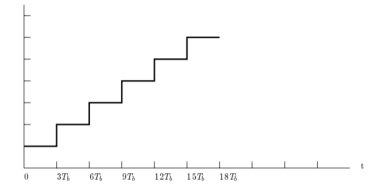
Q1) Figure shows a PCM wave in which the amplitude levels of +1 volt and -1 volts are used to represent binary symbols 1 and 0 respectively. The codeword used consists of three bits. Find the sampled version of an analog signal from which this PCM is derived.
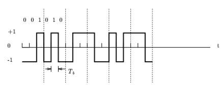
A1) The sample analog signal has the following waveform
Q2) Show that the use of A-law companding provides a ratio of maximum step size to minimum step size equal to the parameter A.
A2)
For the A-law companding we have
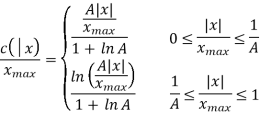
For small input x, the A-law is characterized by its derivatives:

For large input on the other hand it is characterized by

Accordingly

Q3) Consider a DPCM system whose transmitter uses a first order predictor optimized in the minimum mean squared sense. Calculate the prediction gain of the system for the following values of the correlation coefficient for the
(i) 
(ii) 
The correlation coefficient  equals the autocorrelation function of the message signal for the delay T, normalized with respect ot the mean square value of the signal.
(b) Suppose that the predictor is made suboptimal by setting the coefficient  /calculate the resulting values of the prediction gain for the two values of
 specified in part(a). What is the minimum value of
  for which the suboptimal system produces a prediction gain greater that one?
A3)
(a) The predictor Gain is
 As shown in the class, the prediction error variance
  is related to the variance of the input signal,
 as
as

(i) 

(ii) 

(b) The prediction error is 
Correspondingly the prediction error variance is

Substituting (1) in (2) and simplifying we get

The prediction gain is therefore

(i) 

(ii) 

The minimum value for which the prediction gain in (3) exceeds unity is when the correlation coefficient  is less than 0.5
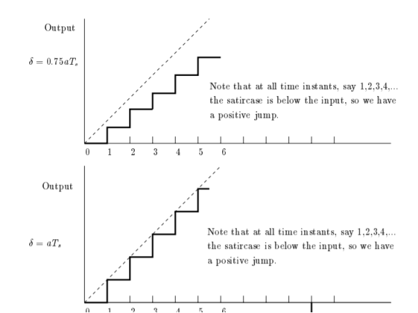
Q4) The ramp signal  is applied to a delta modulator that operates with a sampling period
  , and step size =2δ.
(a) Show slope-overload distortion occurs is δ<
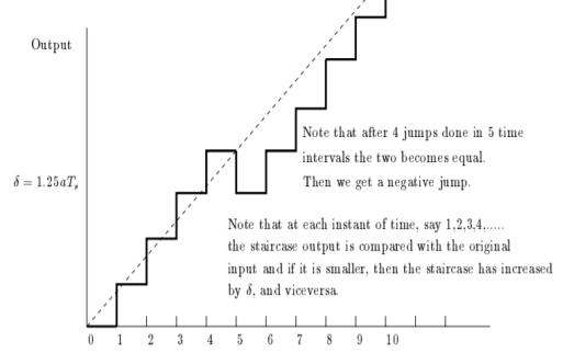
(b) Sketch the modulator output of the following three values of the step size
(i) 
A4)
(a) In a period  , the input signal rises by
 whereas the output of the delta modulator rises by an amount equal to δ/ Hence slope overload distortion occurs if

(b)
For each of the three values of  the modulator output is as shown in fig.
This figure illustrate that slope overload distortion occurs if 
Figure is shown in next question.
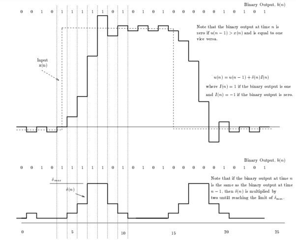
Q5) Consider an adaptive delta modulator. For which the input signal  is given by

The adaption algorithm for the modulator is defined with the constant K equal to 2. The maximum and minimum permissible values of the step size are as follows.


The initial conditions are given by


Plot the stair case approximation  and the binary output for
A5)
Let the sampling period  Then
Then

The binary output,  is equal to zero if
  and is equal to one otherwise
  . This means that
  is one if the binary output is one and is -1, If the binary output is zero


For the reconstruction we have
Resulting in

Initial conditions


Using these initial conditions and input in the defining relations for the adaptive delta modulation ,we get the approximation u(n), the adaptive variation of  , and the resulting binary output b(n) as shown in fig.
Q6) A Delta modulated system is designed to operate at five times the Nyquist Rate. The signal bandwidth B at its input port is 3 kHz and the quantized step is 250 millivolts (0.25 volt). For this problem we assume a 2 kHz sinusoidal input – Find the maximum amplitude Am of this 2 kHz tone.
A6) We know that B = 3 kHz, fm = 2 kHz and = 250 mV.
The Nyquist rate is 3,000 2 = 6,000 Hz. So, five time the Nyquist rate is 30,000 Hz = fs.
Using the relationship

Q7) A one kilohertz (1 kHz) signal m(t) is sampled at 8 kHz with 12-bit encoding for PCM transmission.
(a) How many bits are transmitted per second in in PCM? What is the bandwidth required in this case?
(b) Now switch to using DM with 8 kHz sampling. How many bits are transmitted per second using DM? What is the bandwidth required in using DM?
A7) We know that the signal frequency is fm = 1 kHz and the sampling rate is 8 kHz.
(a) For PCM we have 8,000 samples per second and 12 bits per sample; which equals 96,000 bits/second. The bandwidth is one-half of this giving 48,000 Hz.
(b) Now for DM we have 1 bit per sample at 8,000 samples per second. Thus, we have 8,000 bits per second and a bandwidth of 4,000 Hz.
Comparison
S.No | Parameter of comparison | Pulse code Modulation (PCM) | Delta Modulation (DM) | Adaptive Delta modulation (ADM) | Differential pulse code modulation (DPCM) |
1. | Number of bits | It can use 4, 8 or 16 bits per sample. | It uses only one bit for the sample | It uses only one bit for one sample | Bits can be more than one but are less than PCM. |
2. | Levels and step size | The number of levels depends on number of bits. Level size is fixed. | Slope size is kept fixed and cannot be varied. | According to signal variation step size varies. | The number of levels is fixed. |
3. | Quantization error and distortion | Quantization error depends on number of levels used. | Slope overload distortion and granular noise are present. | Quantization noise is present but other errors are absent. | Slope overload distortion and Quantization noise is present. |
4. | Transmission bandwidth | Highest bandwidth is required since number of bits are high. | Lowest bandwidth is required. | Lowest bandwidth is required. | Bandwidth required is less than PCM. |
5. | Feedback | There is no feedback in transmitter or receiver. | Feedback exists in transmitter | Feedback exists. | Feedback exists. |
The type of modulation, where the sampling rate is much higher and in which the step size after quantization is of a smaller value Δ, such a modulation is termed as delta modulation.
Features
- The quality is moderate.
- The design of the modulator and the demodulator is simple.
- The stair-case approximation of output waveform.
- The step-size is very small, i.e., Δ delta.
- The bit rate can be decided by the user.
- This involves simpler implementation.
Delta Modulation is a simplified form of DPCM technique, also viewed as 1-bit DPCM scheme. As the sampling interval is reduced, the signal correlation will be higher.
Delta Modulator
The Delta Modulator comprises of a 1-bit quantizer and a delay circuit along with two summer circuits. Following is the block diagram of a delta modulator.
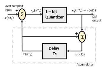
Fig 17: Delta Modulator
The predictor circuit in DPCM is replaced by a simple delay circuit in DM.
From the above diagram, we have the notations as −
- x (n Ts)= over sampled input
- Ep (n Ts) = summer output and quantizer input
- Eq (n Ts) = quantizer output = v (n Ts)
- xˆ (n Ts) = output of delay circuit
- u (n Ts) = input of delay circuit
Using these notations, now we shall try to figure out the process of delta modulation.
Ep(nTs)=x(nTs)−xˆ(nTs) ---------equation 1
=x(nTs)−u([n−1] Ts
=x(nTs)−[xˆ[[n−1] Ts] +v[[n−1] Ts]] -------equation 2
Further,
v(nTs)=eq(nTs)=S.sig. [ep(nTs)] ---------equation 3
u(nTs)=xˆ(nTs)+eq(nTs)
Where,
- xˆ(nTs) = the previous value of the delay circuit
- Eq(nTs) = quantizer output = v(nTs)
Hence,
u(nTs)=u([n−1] Ts) +v(nTs)---------equation 4
Which means,
The present input of the delay unit
= The previous output of the delay unit + the present quantizer output the present quantizer output
Assuming zero condition of Accumulation,

Accumulated version of DM output =  --------equation 5
Now, note that
xˆ(nTs)=u([n−1] Ts)
= ---------equation 6
Delay unit output is an Accumulator output lagging by one sample.
From equations 5 & 6, we get a possible structure for the demodulator.
A Stair-case approximated waveform will be the output of the delta modulator with the step-size as delta (Δ). The output quality of the waveform is moderate.
Delta Demodulator
The delta demodulator comprises of a low pass filter, a summer, and a delay circuit. The predictor circuit is eliminated here and hence no assumed input is given to the demodulator.
Following is the diagram for delta demodulator.
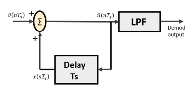
Fig 18. Delta Demodulator
From the above diagram, we have the notations as −
- vˆ(nTs) is the input sample
- uˆ(nTs) is the summer output
- x¯(nTs) is the delayed output
A binary sequence will be given as an input to the demodulator. The stair-case approximated output is given to the LPF.
Low pass filter is used for many reasons, but the prominent reason is noise elimination for out-of-band signals. The step-size error that may occur at the transmitter is called granular noise, which is eliminated here. If there is no noise present, then the modulator output equals the demodulator input.
Advantages of DM Over DPCM
- 1-bit quantizer
- Very easy design of the modulator and the demodulator
Key takeaway
The type of modulation, where the sampling rate is much higher and in which the step size after quantization is of a smaller value Δ, such a modulation is termed as delta modulation.
Limitations of DM
Delta modulation is subject to rate of rise over load problems whenever the input changes too rapidly for the stepped wave form to follow it. If the input signal level remains constant, the reconstructed Delta modulation waveform exhibits a hunting behaviour known as idling noise. This idling noise is a square wave at one half the clock rate. If the clock rate is much greater than twice the highest frequency in the input signal, most of the idling noise can be filtered out at the receiver.
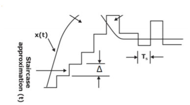
Fig 19. Slope Overload
Slope Overload: Slope overload distortion occurs when the analog input signal changes at a faster rate than the DAC can maintain it, the slope of the analog signal is greater than the delta modulator can maintain. In general, when the slope of stair case is less than (or) equal to modulating signal, the slope overloading occurs. Increasing the clock frequency reduces the probability of slope overload occurring. General method to reduce the slope overload is to increase the magnitude of the size. Assume the input for Delta modulation be f(t) = A cos ωmt.

If the step size used in the Delta modulation system is ‘Δ’, then the maximum (rate of rise) slope over load is / Ts


Granular noise: In general, Granular noise occurs
- When the original analog input signal has a relatively constant amplitude, the reconstructed signal has variations that were not present in the original signal. This is called granular noise
- The granular noise is analogous to the quantization noise in a PCM system.
- When the step size Δ is too large relative to the local slope characteristics of the input waveform x(t), thereby causing the stair case approximation u(t) to hunt around a relatively flat segment of the input waveform Granular noise can be reduced by decreasing the step size so that the stair case approximation may become more closer to the modulating signal.
There is a need to have a large step size to accommodate a wide dynamic range, whereas small step size is required for the accurate representation of relatively low-level signals.


Therefore, a granular noise can be removed by taking a small resolution of step size and a slope over load distortion can be removed by taking a large resolution.
Key takeaway
The input for Delta modulation be f(t) = A cos ωmt.
Slope=
Adaptive Delta Modulation
In digital modulation, we have come across certain problem of determining the step-size, which influences the quality of the output wave.
A larger step-size is needed in the steep slope of modulating signal and a smaller step size is needed where the message has a small slope. The minute details get missed in the process. So, it would be better if we can control the adjustment of step-size, according to our requirement in order to obtain the sampling in a desired fashion. This is the concept of Adaptive Delta Modulation.
Following is the block diagram of Adaptive delta modulator.
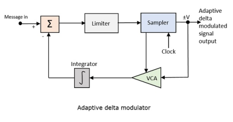
Fig. 20 Adaptive delta modulator
The gain of the voltage-controlled amplifier is adjusted by the output signal from the sampler. The amplifier gain determines the step-size and both are proportional.
ADM quantizes the difference between the value of the current sample and the predicted value of the next sample. It uses a variable step height to predict the next values, for the faithful reproduction of the fast-varying values.
Key takeaway
ADM quantizes the difference between the value of the current sample and the predicted value of the next sample. It uses a variable step height to predict the next values
There are two types of Quantization - Uniform Quantization and Non-uniform Quantization.
The type of quantization in which the quantization levels are uniformly spaced is termed as a Uniform Quantization. The type of quantization in which the quantization levels are unequal and mostly the relation between them is logarithmic, is termed as a Non-uniform Quantization.
Companding
It is a combination of Compressing and Expanding, which means that it does both. This is a non-linear technique used in PCM which compresses the data at the transmitter and expands the same data at the receiver. The effects of noise and crosstalk are reduced by using this technique.
There are two types of Companding techniques. They are −
1. A-law Companding Technique
- Uniform quantization is achieved at A = 1, where the characteristic curve is linear and no compression is done.
- A-law has mid-rise at the origin. Hence, it contains a non-zero value.
- A-law companding is used for PCM telephone systems.
2. µ-law Companding Technique
- Uniform quantization is achieved at µ = 0, where the characteristic curve is linear and no compression is done.
- µ-law has mid-tread at the origin. Hence, it contains a zero value.
- µ-law companding is used for speech and music signals.
- µ-law is used in North America and Japan.
Key takeaway
A-law Companding Uniform quantization is achieved at A = 1, where the characteristic curve is linear and no compression is done.
References:
1. P Ramkrishna Rao, Digital Communication, McGraw-Hill Publication
2. J.G. Proakis, Digital Communication.
3. S. Haykin, Communication Systems
4. Leon W. Couch: Analog/Digital Communication, 5thEdition, PHI,2008