Unit - 1
Introduction to Operational Amplifier
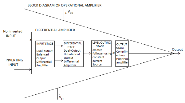
Fig 1 Block Diagram of Operational Amplifier (Op-Amp)
- The op-amp begins with a differential amplifier stage, which operates in the differential mode. Thus the inputs noted with ‘+’ & ‘- ‘ .
- The positive sign is for the non-inverting input and negative is for the inverting input.
- The non-inverting input is the ac signal (or dc) applied to the differential amplifier which produces the same polarity of the signal at the output of op-amp.
- The inverting signal input is the ac signal (or dc) applied to the differential amplifier. This produces 180 degrees out of phase signal at the output.
- The inverting and non-inverting inputs are provided to the input stage which is a dual input, balanced output differential amplifier.
- The voltage gain required for the amplifier is provided in this stage along with the input resistance for the op-amp.
- The output of the initial stage is given to the intermediate stage, which is driven by the output of the input stage.
- In this stage direct coupling is used, which makes the dc voltage at the output of the intermediate stage above ground potential. Therefore, the dc level at its output must be shifted down to 0Volts with respect to the ground.
- For this, the level shifting stage is used where usually an emitter follower with the constant current source is applied.
- The level shifted signal is then given to the output stage where a push-pull amplifier increases the output voltage swing of the signal and also increases the current supplying capability of the op-amp.
Key takeaway
- The inverting signal input is the ac signal (or dc) applied to the differential amplifier. This produces 180 degrees out of phase signal at the output.
- The inverting and non-inverting inputs are provided to the input stage which is a dual input, balanced output differential amplifier.
Differential Amplifier is a device which is used to amplify the difference between the voltages applied at its inputs. Such circuits can be of two types viz.,
- Differential amplifiers built using transistors, either BJT or FET
- Differential amplifiers built using Op-Amps.
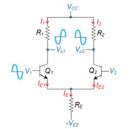
Figure 2. BJT Differential Amplifier
Here the input signals (V1 and V2) are applied to the base of the transistors while the output is collected across their collector terminals (Vo1 and Vo2).
- If V1 at Q1 is sinusoidal, then as V1 goes on increasing, the transistor starts to conduct and this results in a heavy collector current IC1 increasing the voltage drop across RC1, causing a decrease in Vo1.
- Due to the same effect, even IE1 increases which increases the common emitter current, IE resulting in an increase of voltage drop across RE.
- This means that the emitters of both transistors are driven towards positive which in turn implies that the base of Q2 would start to become more and more negative.
- This results in a decrease of collector current, IC2 which in-turn decreases the voltage drop across the collector resistor RC2, resulting in an increase in the output voltage Vo2.
- This indicates that the changes in the sinusoidal signal observed at the input of transistor Q1 is reflected as such across the collector terminal of Q2 and appear with a phase difference of 180o across the collector terminal of Q1.
- The differential amplification can be driven by considering the output in-between the collector terminals of the transistors, Q1 and Q2.
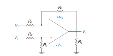
Figure. 3 Differential Amplifier using Op-amp
Here V1 and V2 represent the voltages applied at its inverting and non-inverting input terminals and Ad refers to its differential gain.
The output of the differential amplifier is given as
Vo = Ad (V1 – V2) + Ac (V1 + V2/2)
Where AC is called the common mode gain of the amplifier.
Hence its output voltage will be equal to the sum of the output voltages produced by the Op-Amp circuit operating as an inverting amplifier and the Op-Amp circuit operating as a non-inverting amplifier.
Thus, one gets,
Vo = -Rf/R1 V1 + V2. Rf / R2 + R3 (1 + Rf/R1)
Now, if R1 = R2 and R3 = Rf, then
Vo = -Rf/R1 V1 + V2 . Rf/ R1 + Rf ( R1 + Rf/R1)
Vo = - Rf/R1 . V1 + V2 . Rf /R1
Vo = - Rf/R1 (V1 – V2)
This implies that the gain of the differential amplifier circuit is given by -Rf/R1.
Key takeaway
Ideal Inverting amplifier | Ideal non-inverting amplifier |
1. Voltage gain  | 1. Voltage gain  |
2.The output is inverted with respect to input | 2. No phase shift between input and output |
3. The voltage gain can be adjusted as greater than, equal to or less than one | 3. The voltage gain is always greater than one |
4. The input impedance is  | 4. The input impedance is very large. |
Input voltage
The circuit is designed to have a VCE of 5V across Q2 and Q4. With a ±10 V supply and the bases of Q1 and Q2 at ground level, the voltage drops across R1 and R4 is 5.7 V and 4.3 V respectively. If the input voltage at Q1 base goes down to -4 V, the output terminal and Q2 base also goes down to -4 V as the output follows the input.
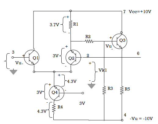
Fig 2 Input Voltage
This means that the emitter terminals of Q1 and Q2 are pushed down from -0.7 to -4.7 V. Consequently, the collector of Q4 is pushed down by 4 V, reducing VCE4 from 5 V to 1 V. Although Q4 might still be operational with a VCE of 1 V, it is close to saturation. It is seen that there is a limit to the negative going input voltage that can be applied to the op-amp if the circuit is to continue to function correctly.
There is also a limit to positive going input voltages. Where VB1 goes to +4 V, the voltage drop across resistor R1 must be reduced to something less than 1 V, in order to move VB2 and VE3 up by 4 V to follow the input. This requires a reduction in Ic2 to a level that makes Q2 approach cut-off. The input voltage cannot be allowed to become large enough to drive Q2 into cut-off
Output Voltage
The maximum voltage swing is limited by the input voltage range. The output voltage can swing in a positive or negative direction depends on the supply voltage and the op-amp output circuitry. The output voltage should be able to rise until Q5 is near saturation and fall until Q6 approaches saturation.
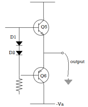
Fig 3 output voltage
But because of the circuits that control the output stage, is normally not possible to drive the output transistors close to saturation levels. A rough approximation for most op-amps is that the maximum output voltage swing is approximately equal to 1 V less than the supply voltage. For the 741 op-amp with a supply of ±15 V, the data sheet lists the output voltage swing as typically ±14 V.
Offset voltages
With an input offset voltage and a differential input circuit, ideal op-amps and comparators will have an offset voltage of 0V, including error voltage.
When inputting a common-mode (same) voltage to the input pins of an op-amp or comparator, with an ideal op-amp no output voltage will be output
In case where an input offset voltage exists, a voltage will be output based on the input offset voltage. This input offset voltage, which is the differential voltage required to make the output voltage 0V, becomes the input conversion value.
The Offset voltage is normally expressed in units of mV or µV. Values closer to 0 are more ideal.
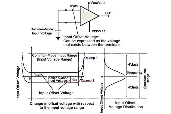
Fig 4 Op-Amp Parameters
The output offset voltage is the voltage at the output when the differential input voltage is zero.
Offset currents
Bias current compensation will work if both bias currents IB+ and IB- are equal. Since the input transistor cannot be made identical. There will always be some small
Difference between IB+ and IB-. This difference is called the offset current
|Ios| = IB+-IB------------------------- (7)
Offset current Ios for BJT op-amp is 200nA and for FET op-amp is 10pA. Even with bias current compensation, offset current will produce an output voltage when Vi = 0.
V1 = IB + R comp
And I1 = V1 R1
KCL at node a gives
I2 = (  – I1) =
  - ( Ib + Rcomp/R1 )
Again V0 = I2 Rf – V1
Vo = I2 Rf - IB+ Rcomp
Vo = 1M Ω X 200nA
Vo = 200mV with Vi = 0
Input and Output Impedance
The input impedance of op-amp is given as
Zif = (1+A )Zi
)Zi
Where:
A = Gain of op-amp
 = Feedback factor
Zi = Input impedance without feedback
The output impedance is given as
Zout = Z0/(1+A )
)
Zo = output impedance of op-amp
CMRR
It is the ratio of differential voltage gain Ad to the common mode voltage gain Acm.
CMRR = 
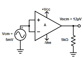
Fig 5 Common Mode Configuration
The common mode voltage gain from above figure can be
 =
= 
Where:
Vocm = output common mode voltage
Vcm = input common mode voltage
Acm = common mode voltage gain
In normal cases the value of Ad is large and Acm is very small making the value of CMRR very high.
Key takeaway
The common mode voltage gain from above figure can be
 =
= 
PSRR
The Power Supply Rejection Ratio (PSRR) is also known as Supply Voltage Rejection Ratio (SVRR). It is defined as the change in op-amps input offset voltage due to variations in the supply voltage.
PSRR = 
 = Change in input offset voltage
 = Change in supply voltage
Slew rate
The slew rate is a parameter that describes the operating speed of an op-amp. It represents the rate that can change per unit time stipulated by the output voltage.
For example, 1V/us indicates that the voltage can change by 1V in 1us. Ideal op-amps make it possible to faithfully output an output signal for any input signal. However, in reality slew rate limits do exist.
When supplying a rectangular pulse at the input with a steep rise and fall, this indicates the possible degree of change in the output voltage per unit time.

Fig 6 Voltage Follower
The rise and fall slew rates are calculated by the following equations:
SRr = ∆ V / ∆ Tr
SRf = ∆ V / ∆ Tf
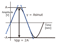
Fig 7 Slew Rate Calculation
Calculate the slew rate
The output is given by
y=Asinωt
The slew rate is the slope of the tangent of the sine wave, differentiating the above equation.
Dy / Dt = Aω cosωt ωt=0
The slew rate is
SR=Aω ω=2πf
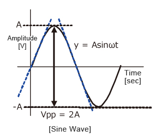
Fig 8 Sine wave amplitude
Since the amplitude of the sine wave becomes Vpp=2A (peak-to-peak), the equation can be modified as follows.

This frequency(f) is referred to as the full power bandwidth. These are conditions where the amplification factor in the op-amp has not been set, in other words the relationship of the frequency and amplitude (within the output voltage range) that can be output by the op-amp in a voltage follower circuit.
Key takeaways
Slew rate is the maximum rate of output voltage change per unit time. It is denoted by S. For getting undistorted output voltage we must have very high slew rate. It is measured in V/sec.
Frequency limitations
Fig below shows the graph of open loop gain (A) plotted versus frequency (f) for a 741 op-amp. f = 100 Hz, A = 80 dB f = 1 KHz, A = 60 dB
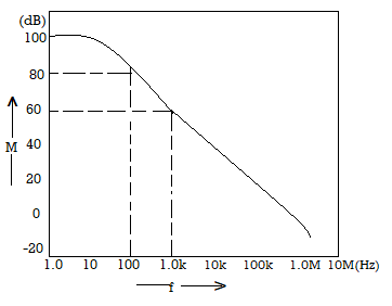
Fig 9 Frequency Response
The open loop gain (A) falls by 20 dB when the frequency increases from 100 Hz to 1 KHz. The ten times increase in frequency is termed a decade. So, the rate of the gain is said to be 20 dB per decade. Where internal gain equals to or greater than 80 dB is required for a particular application, it is available with a 741 only for signal frequencies up to ≈100 Hz. A greater than 20 dB is possible for signal frequencies up to ≈ 90 kHz. Other op-amp maintains substantial 1.3 OP-AMP AS DC AMPLIFIERS: Biasing op-amps internal gain to much higher frequencies than the 741
An Op-Amp has a very high gain typically order of 10 5. If power supply voltage Vcc =15V. Then maximum input voltage which can be applied
Vd = Vcc /Ad = 15/ 105 = 150 µ V
i.e. Op -Amp can work as a linear amplifier (from +Vi to –Vi) if input voltage is less than 150 µV.
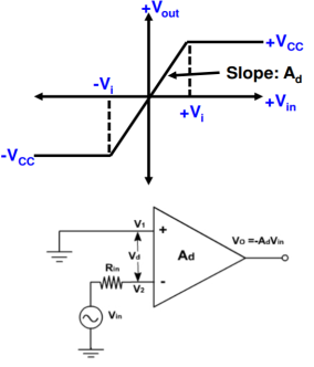
If V1 is grounded then V2 cannot be more than 150 µV which is very small and close to ground. Therefore, V2 can also be considered at ground if V1 is at ground. Physically V 2 is not connected to the ground yet we considered V2 at ground that is called virtual ground.
An Operational Amplifier is basically a three-terminal device which consists of two high impedance inputs. One of the inputs is called the Inverting Input, marked with a negative or “minus” sign, ( – ). The other input is called the Non-inverting Input, marked with a positive or “plus” sign (+).
A third terminal represents the operational amplifiers output port which can both sink and source either a voltage or a current.
In a linear operational amplifier, the output signal is the amplification factor, known as the amplifiers gain ( A ) multiplied by the value of the input signal and depending on the nature of these input and output signals, there can be four different classifications of operational amplifier gain.
- Voltage – Voltage “in” and Voltage “out”
- Current – Current “in” and Current “out”
- Transconductance – Voltage “in” and Current “out”
- Transresistance – Current “in” and Voltage “out”

Fig 2 Operational Amplifier
Practical op-amps have zero offset voltage. The bandwidth of the practical op-amp is very small. This output can be raised to the required value by adjusting the negative feedback. The equivalent circuit is shown below.

Fig 3 Practical Op-Amp
The input impedance Zi ranges to mega ohms. The output impedance Z0 is in the order of ohms and the practical op-amps have high value of open loop voltage gain AV. The value of CMRR and Slew rate should be as high as possible.
Key takeaway
For ideal Op-Amp
Open loop gain = 
Input Resistance = 
Output Resistance =0
Offset voltage = 0
Bandwidth of operation = 
An Operational Amplifier is basically a three-terminal device which consists of two high impedance inputs. One of the inputs is called the Inverting Input, marked with a negative or “minus” sign, ( – ). The other input is called the Non-inverting Input, marked with a positive or “plus” sign (+).
A third terminal represents the operational amplifiers output port which can both sink and source either a voltage or a current.
In a linear operational amplifier, the output signal is the amplification factor, known as the amplifiers gain ( A ) multiplied by the value of the input signal and depending on the nature of these input and output signals, there can be four different classifications of operational amplifier gain.
- Voltage – Voltage “in” and Voltage “out”
- Current – Current “in” and Current “out”
- Transconductance – Voltage “in” and Current “out”
- Transresistance – Current “in” and Voltage “out”
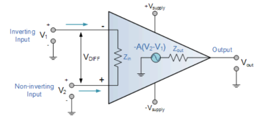
Fig 2 Operational Amplifier
Practical op-amps have zero offset voltage. The bandwidth of the practical op-amp is very small. This output can be raised to the required value by adjusting the negative feedback. The equivalent circuit is shown below.
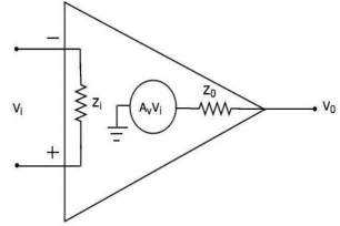
Fig 3 Practical Op-Amp
The input impedance Zi ranges to mega ohms. The output impedance Z0 is in the order of ohms and the practical op-amps have high value of open loop voltage gain AV. The value of CMRR and Slew rate should be as high as possible.
Key takeaway
For ideal Op-Amp
Open loop gain = 
Input Resistance = 
Output Resistance =0
Offset voltage = 0
Bandwidth of operation = 
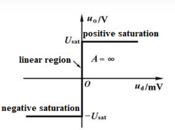
Fig 4 Transfer characteristics of ideal op-amp
Open Loop Gain (Avo)
The main function of an operational amplifier is to amplify the input signal and the more open loop gain it has the better. Open-loop gain is the gain of the op-amp without positive or negative feedback and for such an amplifier the gain will be infinite
Input impedance (ZIN)
Input impedance is the ratio of input voltage to input current and is assumed to be infinite to prevent any current flowing from the source supply into the amplifiers input circuitry ( IIN = 0 ). Real op-amps have input leakage currents from a few pico-amps to a few milli-amps.
Output impedance (ZOUT)
The output impedance of the ideal operational amplifier is assumed to be zero acting as a perfect internal voltage source with no internal resistance so that it can supply as much current as necessary to the load. This internal resistance is effectively in series with the load thereby reducing the output voltage available to the load. Real op-amps have output impedances in the 100-20kΩ range.
Bandwidth (BW)
An ideal operational amplifier has an infinite frequency response and can amplify any frequency signal from DC to the highest AC frequencies, so it is therefore assumed to have an infinite bandwidth.
With real op-amps, the bandwidth is limited by the Gain-Bandwidth product (GB), which is equal to the frequency where the amplifiers gain becomes unity.
Offset Voltage (VIO)
The amplifiers output will be zero when the voltage difference between the inverting and the non-inverting inputs is zero, the same or when both inputs are grounded. Real op-amps have some amount of output offset voltage.
Key takeaway
High input resistance
Lower output resistance
Infinite voltage amplification
Under a certain supply voltage condition, the amplifier can only work in closed-loop (negative feedback) mode.
Non-inverting amplifier
Non- Inverting amplifier is one in which the output is in phase with respect to input that is if you apply a positive voltage, output will be positive. The output is an non -inverted amplified version of input.

Fig 11 Non-Inverting Amplifier
Assuming the op-amp is ideal and applying the concept of virtual short, the voltage at the inverting terminal is equal to non- inverting terminal.
Applying KCL at inverting node we get
Vi -Vo/ R2 + Vo – 0 / R1 = 0
By rearranging the terms, we will get
Voltage gain Av = Vo/ Vi = (1+ Rf/Ri)
Gain of non- inverting amplifier Av= (1+ Rf/Ri).
Example-1
Design a non-inverting amplifier using Op-amp with a closed loop voltage gain of 10.
Af = 1 + Rf/R1 =10
Rf/R1 = 9
Rf = 9 R1
If R1 = 1K
Rf = 9K Ω
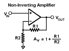
Substitute values in above figure. This is the required non-inverting amplifier circuit
Example-2
In an op-amp inverting amplifier R1 = 1K Ω and Rf = 100KΩ. The DC supply voltage of the op-amp is ± 15V. Calculate the output voltage if input voltage is 1V.
R1 = 1KΩ Rf = 100KΩ
V+ = 15V and V-=-15V. Vi = 1V
Af = -Rf/R1 = -100K/1K = -100
Af = vo/vi
Vo = Af vi
= -100 x 1V = -100V
The output voltage cannot exceed the DC power supply voltage . Since vo is negative and large it is limited to V-
Vo ≈ V- = -15V
Inverting Amplifier
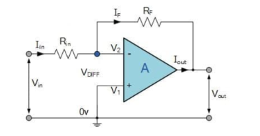
Fig 12 Non-Inverting Amplifier
The input signal vi is applied to the inverting input terminal through resistor R1 and non-inverting input terminal is grounded. The feedback from the output of the inverting terminal is provided through the feedback resistor Rf.
Since the input is applied to the inverting terminal vo and vi are opposite in polarity and hence the feedback is negative. Since the non-inverting input terminal is grounded v2=0. Due to virtual short at the input of op-amp the inverting and non-inverting input terminals are at the same potential.
Therefore, v1 = v2 = 0.
Due to high input impedance of Op-amp the current flowing into its inverting input terminal is zero. Therefore, the same current flows through R1 and Rf.
i 1 = i f
But i1 = vi – v1 / R1 = vi/R1
i f = v1 – vo / Rf = -vo/Rf
Vi/R1 = - vo/Rf
Af = vo/vi = -Rf/R1
Af is the closed loop voltage gain or voltage gain with negative feedback.
Example
A 200mV peak to peak sine waveform voltage is applied to Op-amp inverting amplifier with Rf/R1 = 10.
Solution
Peak to peak input voltage
2Vm = 200 mV
Vm = 100 mV
Vi= Vm sin wt = 100 sin wt mV
Vo = -Rf/R1 x vi = -10 x 100 sinwt mV
= -1000 sin wt mV
References:
1. David A. Bell, ‘Op-amp & Linear ICs’, Oxford, 2013.
2. D. Roy Choudhary, Sheil B. Jani, ‘Linear Integrated Circuits’, II edition, New Age, 2003.
3. Ramakant A. Gayakward, ‘Op-amps and Linear Integrated Circuits’, IV edition, Pearson Education, 2003 / PHI. 2000.
4. N. C. Goyal and Khetan ‘A Monograph on Electronics Design Principals’, Khanna Publications
5. Sergio Franco, “Design with Operational Amplifiers and Analog Integrated Circuits”, McGraw Hill.