Unit - 2
OP-AMP Linear Applications
A voltage follower (also called a unity-gain amplifier, a buffer amplifier, and an isolation amplifier) is a op-amp circuit which has a voltage gain of 1.
This means that the op amp does not provide any amplification to the signal. The reason it is called a voltage follower is because the output voltage directly follows the input voltage, meaning the output voltage is the same as the input voltage. Thus, for example, if 10V goes into the op amp as input, 10V comes out as output. A voltage follower acts as a buffer, providing no amplification or attenuation to the signal.

Fig.:1 Voltage follower
Inverting Summing Amplifier
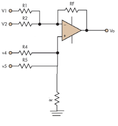
Fig 2: Summing amplifier
- In the above figure, each terminal is connected with two input sources through resistors. V1 and V2 is connected to the inverting terminal and V4 and V5 is connected to the non-inverting terminal.
- Assuming R1=R2=R4=R5=RF=R.
- Now, on applying superposition theorem, for finding output voltage due to V1 alone, keep V2=V4=V5=0V.
- Hence, now the circuit acts as an inverting amplifier.
- Therefore,

- Similarly,

- Now, for V4, voltages V1=V2=V5=0V then the circuit behaves as a non-inverting amplifier.


Hence,


Similarly,

So, the resultant output voltage by all the 4 input voltages is given by,
Vo = V01 + V02 + V04 +V05
Vo = -V1 – V2 +V4 + V5
The output voltage Vo is equivalent to the sum all input voltages applied at both the terminals.
Example 1:
In a summing amplifier, if R = 1kΩ, Va = +3V, Vb = +8V, Vc = +9V, Vd = +5V and supply voltage is ±15V. Find the output voltage Vo.
Solution:
Vo = Sum of all input voltages applied at both the terminals
Vo = Va + Vb + Vc +Vd
Vo = -3 -8 +9 +5
Vo = +3V
Example 2:
Find the output voltage for the given circuit diagram if Rf = 5kΩ.
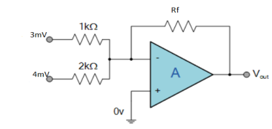
Solution:
We know,
Gain (Av) = =
= 
Hence,
Av1 = 
Av2 = 
Now, Output voltage Vo = Sum of the two amplified input signals
Vo = Av1 x V1 + Av2 x V2
Vo =(-5 x 3) + ( -2.5x 4) mV
Vo = -25mV
As the above output voltage is negative hence it is an inverting amplifier.
Non-Inverting
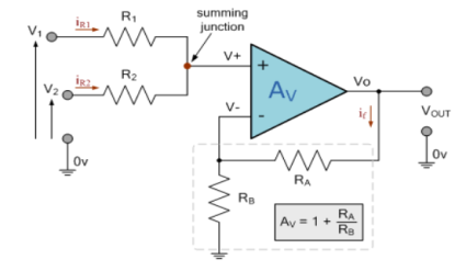
Fig 3: Non-Inverting Summing Amplifier
Applying KCL to the above circuit we have
IR1+IR2 = 0
 =
=  = 0
= 0
When R1 = R2 =R
V+ = 
The voltage gain for non-inverting summing amplifier is given as
AV = Vout/Vin =  = 1+
= 1+
Vout= [1+ ]
] 
Key takeaway
AV = Vout/Vin =  = 1+
= 1+
Vout= [1+ ]
] 
This circuit multiplies each input by a factor (the factor is determined by circuit design) and then adds these values together. The factor that is used to multiply each input is determined by the ratio of the feedback resistor to the input resistor. For example, you could design a circuit that would produce the following output from three inputs (E1, E2, E3):

Using input resistors R1 for input number one (E1), R2 for input number two (E2), R3 for input number three (E3), and R4 for the feedback resistor, you could calculate the values for the resistors:


Any resistors that will provide the ratios shown above could be used. If the feedback resistor (R4) is a 12-kilohm resistor, the values of the other resistors would be:
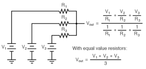
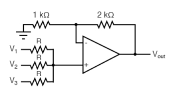
Fig.4: Averaging amplifier
Numerical:
Calculate the currents and voltages as done for the previous circuits. With:

Solution:


The Instrumentation amplifiers consist of three op-amps. In this circuit, a non-inverting amplifier is connected to each input of the differential amplifier.
This instrumentation amplifier provides high input impedance for exact measurement of input data from transducers. The circuit diagram of an instrumentation amplifier is as shown in the figure below.
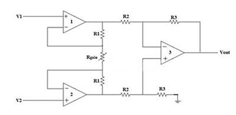
Fig 5 Instrumentation Amplifier
The op-amps 1 & 2 are non-inverting amplifiers and together form an input stage of the instrumentation amplifier. The op-amp 3 is a difference amplifier that forms the output stage of the instrumentation amplifier.
Working
The output stage of the instrumentation amplifier is a difference amplifier, whose output Vout is the amplified difference of the input signals applied to its input terminals.
If the outputs of op-amp 1 and op-amp 2 are Vo1 and Vo2 respectively, then the output of the difference amplifier is given by,
Vout = (R3/R2) (Vo1-Vo2)
The expressions for Vo1 and Vo2 can be found in terms of the input voltages and resistances.
Consider the input stage of the instrumentation amplifier as shown in the figure below.
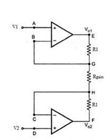
Fig 6 Input Stage of Instrumentation Amplifier
The potential at node A is the input voltage V1. Hence the potential at node B is also V1, from the virtual short concept. Thus, the potential at node G is also V1.
The potential at node D is the input voltage V2. Hence the potential at node C is also V2, from the virtual short. Thus, the potential at node H is also V2.
Ideally the current to the input stage op-amps is zero. Therefore, the current I through the resistors R1, Rgain and R1 remains the same.
Applying Ohm’s law between the nodes E and F,
I = (Vo1-Vo2)/(R1+Rgain+R1) ——————— 1
I = (Vo1-Vo2)/(2R1+Rgain)
Since no current is flowing to the input of the op-amps 1 & 2, the current I between the nodes G and H can be given as,
I = (VG-VH)/Rgain = (V1-V2)/Rgain ————————- 2
Equating equations 1 and 2,
(Vo1-Vo2)/(2R1+Rgain) = (V1-V2)/Rgain
(Vo1-Vo2) = (2R1+Rgain) (V1-V2)/Rgain —————— 3
The output of the difference amplifier is given as,
Vout = (R3/R2) (Vo1-Vo2)
Therefore, (Vo1 – Vo2) = (R2/R3) Vout
Substituting (Vo1 – Vo2) value in the equation 3, we get
(R2/R3) Vout = (2R1+Rgain) (V1-V2)/Rgain
i.e. Vout = (R3/R2) {(2R1+Rgain)/Rgain} (V1-V2)
The above equation gives the output voltage of an instrumentation amplifier. The overall gain of the amplifier is given by the term (R3/R2) {(2R1+Rgain)/Rgain}.
Advantages
- The gain of a three op-amp instrumentation amplifier circuit can be easily varied and controlled by adjusting the value of Rgain without changing the circuit structure.
- The gain of the amplifier depends only on the external resistors used. Hence, it is easy to set the gain accurately by choosing the resistor values carefully.
- The input impedance of the instrumentation amplifier is dependent on the non-inverting amplifier circuits in the input stage. The input impedance of a non-inverting amplifier is very high.
- The output impedance of the instrumentation amplifier is the output impedance of the difference amplifier, which is very low.
- The CMRR of the op-amp 3 is very high and almost all of the common mode signal will be rejected.
Applications
- These amplifiers mainly involve where the accuracy of high differential gain is required, strength must be preserved in noisy surroundings, as well as where huge common-mode signals are there. Some of the applications are
- Instrumentation amplifiers are used in data acquisition from small o/p transducers like thermocouples, strain gauges, measurements of Wheatstone bridge, etc.
- These amplifiers are used in navigation, medical, radar, etc.
- These amplifiers are used to enhance the S/N ratio (signal to noise) in audio applications like audio signals with low amplitude.
- These amplifiers are used for imaging as well as video data acquisition in the conditioning of high-speed signal.
- These amplifiers are used in RF cable systems for amplification of the high-frequency signal.
Key takeaways
This instrumentation amplifier provides high input impedance for exact measurement of input data from transducers. The output impedance of the instrumentation amplifier is the output impedance of the difference amplifier, which is very low.
Integrator
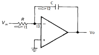
Fig 7: Integrator
- It is a circuit which provides output voltage Vo as an integral form of input voltage Vin.
- It is obtained by using an inverting amplifier and replacing its feedback resistor Rf with a capacitor C.
- Hence,

Ignoring I3 we have, I3 ≈ 0
So, I1 ≈ I2.
- We know current across the capacitor is given by,

- Now by applying Kirchoffs current law,

However, V = 0 because gain A is very large

Integrating both sides we get


 + Q
+ Q
Where Q is the integration constant and is proportional to Vo at t = 0 sec.
Therefore, voltage Vo is directly proportional to Vin and inversely proportional to constant RC.
Frequency response of basic integrator circuit is given by,
 ( for 0 db gain)
Practical integrator with frequency response
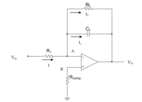
Fig. 8: Practical Integrator
The practical integrator overcomes the limitations of an ideal integrator that uses a resistor Rf , in parallel with Cf . The basic circuit is shown in figure. A compensating resistor is added to compensate for bias current effects. The resistance Rf reduces the low frequency gain of the opamp.


When Rf is very large, then R1 / Rf can be ignored and hence the circuit behaves like an ideal integrator whose output is given by

 (From the output equation)
Replace s by j and let the gain be A, in the steady state, we can write


Where  called as the break frequency of the practical integrator. Thus in the frequency response, dc gain remains constant for all frequencies less than fa and from fa onwards, as frequency increases, gain reduces at a rate of 20 dB / decade.
Magnitude of the gain is given by

At dc condition, (f = 0) we get IAI =Rf/R1
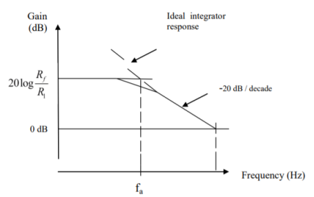
Fig. 9: frequency response
Example-1
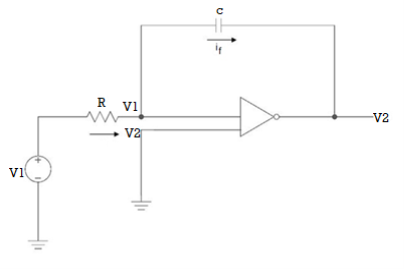
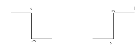
The integrator circuit as shown in the figure has R = 500K Ω and C=1µF. Find and plot the output voltage for the inputs as shown in the figure.
a) b)
c)vi= 2 sin 4tV d) vi= 4tV
Solution:
We know that
v0 = - 1/RC  + v0(0)
Here R= 500K Ω and C = 1µF
1/RC = 1/ 500 x 1000 x 1 x 10-6
= 1/RC = 2
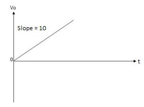
= -2  ; vi =- 5V
= -2 
= 10t V
Which means it is a ramp voltage with positive slope.
When vi=5V
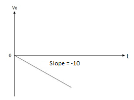
-2  ; vi = 5V
= -2 
= -10t V
Which means it is a ramp voltage with negative slope.
When vi= 2 sin4t V
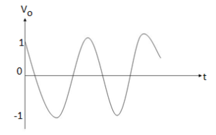
Vo = -2 
= -4 [-cos 4t] /4 = cos 4t
When vi=4t V
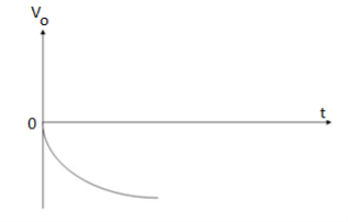
Vo = 
= -8 [t2/2] = - 4V
Key takeaway
 + Q
+ Q
Where Q is the integration constant and is proportional to Vo at t = 0 sec.
4.4 Differentiator
- A differentiator is a circuit that performs differentiation operation. Hence, the output is a derivative of input.
- In an inverting amplifier, if input resistor is replaced by a capacitor then a differentiator circuit is formed.
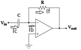
Fig 10: Differentiator
- In the above fig. On applying Kirchhoff’s law we get,

Since Ib = 0 then,
Ic ≈ If

Since Gain A is very large hence, V1 = 0

Or 
- So, the output voltage is RC times the negative rate of change of input voltage.
- When input is a cosine wave, output is a sine wave i.e it performs the inverse function of integrator circuit.
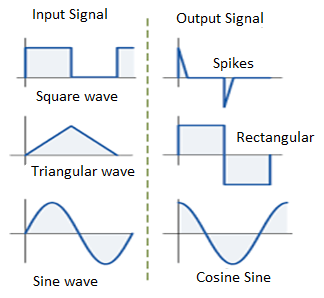
Fig 11: Input and output waveform of differentiator
Frequency response of basic differentiator circuit is given by,
 ( for 0 db gain)
Practical differentiator with frequency response
The noise and stability at high. Frequency can be corrected, in the practical differentiator circuit using the resistance R1 in series with Cl and the capacitor C f in parallel with resistance R f.
The circuit is shown in the Fig. The resistance R comp is used for bias compensation.
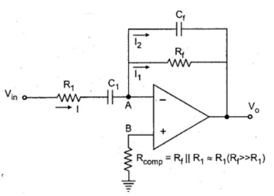
Fig.12: Practical Differentiator
As the input current of op-amp is zero, there is no current input at node B. Hence it is at the ground potential. From the concept of the virtual ground, node A is also at the ground potential and hence VB = VA = 0 V.
For the current I, we can write

Where Z1 = Ri in series with C1
So, in Laplace domain we can write,
 R1 + 1/sC1


Now current I1 is,

In Laplace,


Taking laplace we get,
I2 = -sCf Vo(s)
Applying node analysis at node A
I = I1 + I2


The time constant R 1C1 is much greater than R1C1 or R fC f and hence the equation (20) reduces to,

 as
as 
Thus the output voltage is the RfCi times the differentiation of the input.
It may be noted that though R fel is much larger than RfCf or R1C1, it is less than or equal to the time period T of the input, for the true differentiation.

Applications
- In the wave shaping circuits to detect the high frequency components in the input signal.
- As a rite-of-change detector in the FM demodulators.
- The differentiator circuit is avoided in the analog computers.
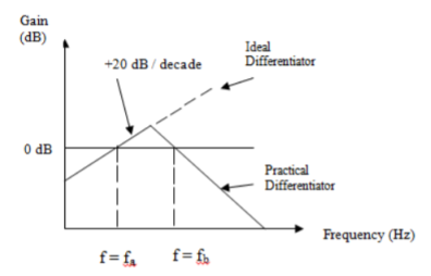
Fig.13: frequency response
Key takeaway
The output voltage for differentiator is 
A current to voltage converter or I to V converter is an electronic circuit that takes current as the input and produces voltage as the output.
An op-amp based current to voltage converter produces an output voltage when current is applied to its inverting terminal. The circuit diagram of an op-amp based current to voltage converter is shown in the following figure.
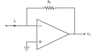
Fig 14. I-V Converter
In the circuit shown above, the non-inverting input terminal of the op-amp is connected to ground. That means zero volts is applied at its non-inverting input terminal.
According to the virtual short concept, the voltage at the inverting input terminal of an op-amp will be equal to the voltage at its non-inverting input terminal. So, the voltage at the inverting input terminal of the op-amp will be zero volts.
The nodal equation at the inverting terminal's node is −
−Ii+0−V0/Rf=0
−Ii=V0/Rf
V0=−Rf.Ii
Thus, the output voltage, V0 of current to voltage converter is the (negative) product of the feedback resistance, Rf and the input current, It. Observe that the output voltage, V0 is having a negative sign, which indicates that there exists a 1800 phase difference between the input current and output voltage.
We can re-write the above equation as −
V0/Ii=−Rf
The above equation represents the ratio of the output voltage V0 and the input current Ii, and it is equal to the negative of feedback resistance, Rf. The ratio of output voltage V0 and input current Ii is called as Trans-resistance.
Key takeaways
A voltage to current converter or V to I converter, is an electronic circuit that takes current as the input and produces voltage as the output.
An op-amp based voltage to current converter produces an output current when a voltage is applied to its non-inverting terminal.
A current to voltage converter or I to V converter is an electronic circuit that takes current as the input and produces voltage as the output.
An op-amp based current to voltage converter produces an output voltage when current is applied to its inverting terminal.
A voltage to current converter or V to I converter, is an electronic circuit that takes current as the input and produces voltage as the output.
An op-amp based voltage to current converter produces an output current when a voltage is applied to its non-inverting terminal. The circuit diagram of an op-amp based voltage to current converter is shown in the following figure.
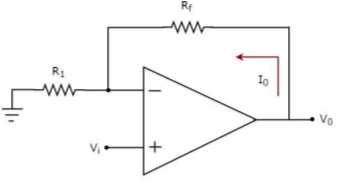
Fig 15. V-I Converter
In the circuit shown above, an input voltage Vi is applied at the non-inverting input terminal of the op-amp.
According to the virtual short concept, the voltage at the inverting input terminal of an op-amp will be equal to the voltage at its non-inverting input terminal .
So, the voltage at the inverting input terminal of the op-amp will be Vi.
The nodal equation at the inverting input terminal's node is −
ViR1−I0=0
=>I0=VtR1
Thus, the output current I0 of a voltage to current converter is the ratio of its input voltage Vi and resistance R1.
We can re-write the above equation as −
I0/Vi=1/R1
The above equation represents the ratio of the output current I0 and the input voltage Vi & it is equal to the reciprocal of resistance R1. The ratio of the output current I0 and the input voltage Vi is called as Transconductance.
Rectifier circuit gives average value of input signal; but in practice we need peak value of input signal. This is achieved by peak detector circuit. The following figure shows a simple peak detector circuit using diode and capacitor.
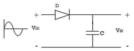
Fig 16. Peak detector
In the positive half cycle, diode D is forward biased and capacitor C starts charging. When input reaches its peak value, capacitor gets charged to positive peak value.
In negative half cycle, as input decreases, diode D is reversed biased and capacitor is isolated and holds the peak value of previous cycle. Hence called as peak detector.
But in practice, output is taken across some load RL, so when input voltage decreases capacitor discharges through load RL. To avoid this, select RL of very large value so that capacitor discharges very slowly hence almost hold the charge. Whatever charge it lost through RL is gets back in next half cycle.
Key takeaway
The diode D is acting as an instant switch, so supply gets loaded.
To avoid the loading while charging capacitor, we use op-amp.
Log Amplifier
As the name says it is an amplifier which produces the output proportional to logarithmic of the applied input. The log amplifier using op-amp is shown below. The input is applied through the inverting end of op-amp. As the non-inverting end has voltage zero then by virtual ground concept the voltage at inverting terminal also becomes zero.
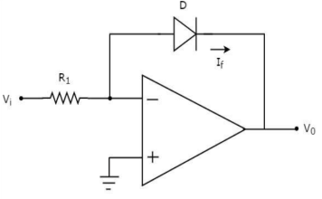
Fig 17. Log Amplifier
The equation for input voltage will be
 +If = 0
If = 
The current flowing through diode is given as

Where:
Is = Saturation Current
Vf = Voltage drop across diode in forward bias
VT = Thermal equivalent voltage
For feedback loop the KVL equation will be
0-Vf -V0 = 0
Vf = -V0
Substituting Vf in above equation of If

Equating both equations of If


Taking natural log of both sides we get


The above equations shows that the output is natural log of the applied input.
Antilog Amplifier
This device produces the output proportional to antilog of input. The inverting op-amp is used in this case as well. The figure below shows an antilog amplifier with its inverting terminal connected to the input end with diode and the non-inverting terminal is grounded.
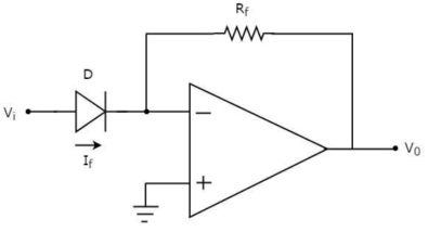
Fig 18. Antilog Amplifier
Applying KCL at input terminal we get


The current flowing through diode is given as

Substituting If in above voltage equation we get


At inverting terminal applying KVL we get


Substituting Vf in equation of V0 we get

The above equations shows that the output is natural antilog of the applied input.
Key takeaways
For Log Amplifier


For Antilog Amplifier

References:
1. David A. Bell, ‘Op-amp & Linear ICs’, Oxford, 2013.
2. D. Roy Choudhary, Sheil B. Jani, ‘Linear Integrated Circuits’, II edition, New Age, 2003.
3. Ramakant A. Gayakward, ‘Op-amps and Linear Integrated Circuits’, IV edition, Pearson Education, 2003 / PHI. 2000.
4. N. C. Goyal and Khetan ‘A Monograph on Electronics Design Principals’, Khanna Publications
5. Sergio Franco, “Design with Operational Amplifiers and Analog Integrated Circuits”, McGraw Hill.