Unit - 3
OP-AMP Non-Linear Applications
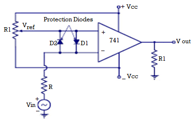
Fig1 Comparator
- A reference voltage Vref of 1V is applied to the inverting terminal of op-amp.
- A time varying voltage Vin is applied to the non-inverting terminal of op-amp.
- Diode D1 and D2 are used to protect the op-amp from damage from excess amount of input voltage Vin.
- They are known as clamp diodes as they clamp the difference input voltage to +0.7V to -0.7V.
- Hence, the above circuit is called as non-inverting Comparator.
Characteristics of comparator
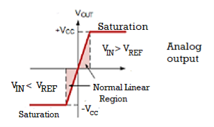
Fig 2 Voltage levels for comparator
- When Vin <Vref, then output Vo = -Vsat (≈ -Vee) because the voltage at negative input is higher than that of positive input.
- When Vin >Vref, then output Vo = +Vsat (≈ +Vee) as the positive input becomes positive with respect to the negative input.
- When Vin ≈ Vref, then Vo changes from one Vsat level to another.
- Therefore the comparator is a type of analog to digital converter.
- It is also known as Voltage Level Detector because for a particular value of Vref, the voltage level of Vin can be detected.
Key takeaway
- When Vin <Vref , then output Vo = -Vsat (≈ -Vee) because the voltage at negative input is higher than that of positive input.
- When Vin >Vref , then output Vo = +Vsat (≈ +Vee) as the positive input becomes positive with respect to the negative input.
The Schmitt Trigger is a logic input type that provides hysteresis or two different threshold voltage levels for rising and falling edge. This is useful because it can avoid the errors when we have noisy input signals from which we want to get square wave signals.
Symmetrical
If we add a positive feedback by connecting the output voltage to the non-inverting input with a resistor between them and another resistor between the VIN and the non-inverting input we will get the Schmitt Trigger. Now the output will switch from VCC– to VCC+ when the voltage at the A node will cross 0 volts.
That means that now by adjusting the values of the resistors we can set at what value of the VIN input the switch will occur using the following equations. We get these equations with the following relationships. The current “i” through this line equals VIN – VA divided by R1 as well as VA – VOUT divided by R2. So if we replace the VA with zero, as we need that value for the switch to occur, we will get that final equation.
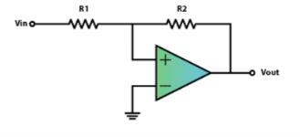
Fig 3 Symmetrical

Va = 0


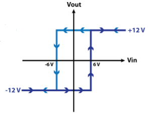
Fig 4 Symmetrical characteristics
Asymmetrical
In order to get two different non-symmetrical thresholds, we can use this circuit of an inverting single powered Schmitt Trigger. Here the VREF voltage is the same as the VCC of the op-amp. Now because the VIN input is connected to the inverting input of the op-amp when its values will reach the upper threshold, the output will switch off to 0 volts, and then when its values will decline to the lower threshold, the output will switch on to 5 volts.
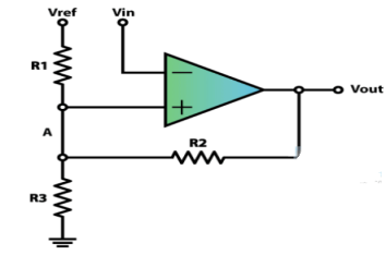
Fig 5 Asymmetrical
Example-1
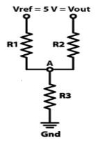
The VREF = VCC = 5 volts and the three resistors will be the same 10k ohms. So calculate the voltage at the A node. Assume Vout =0V and 5V.
Solution:
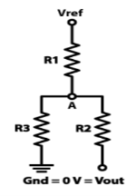
Vout = 0V

Va = 166V
Vout = 5V

Va = 333V
Key takeaway
The Schmitt Trigger is a logic input type that provides hysteresis or two different threshold voltage levels for rising and falling edge. This is useful because it can avoid the errors when we have noisy input signals from which we want to get square wave signals.
The major limitation of conventional rectifiers is that it cannot rectify AC voltages below forward voltage drop VD (0.7V) of a diode. The precision rectifier will make it possible to rectify input voltage of a very small magnitude even less than forward voltage drop of diode. The diode can be used in AM detector where power is negligible and we want information in the signal. Rectifier circuits used for circuit detection with op-amps are called precision rectifiers.
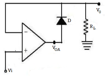
Fig 6 Precision Rectifier
The below figure shows a non-inverting precision rectifier. The diode used is called as precision diode. When the voltage VI is positive the voltage VOA is also positive. When Vi<0the voltage VOA becomes negative and hence reverse biasing the diode and making Vo =0.
When the value of input voltage Vi< (cut-in voltage). The diode again becomes reverse biased as VOA becomes negative. The op-amp then comes to negative saturation. There is no current through RL and V0= 0.
When the value of input voltage Vi> (cut-in voltage) the circuit acts as voltage follower and the output voltage follows the input voltage during this positive half cycle of input.
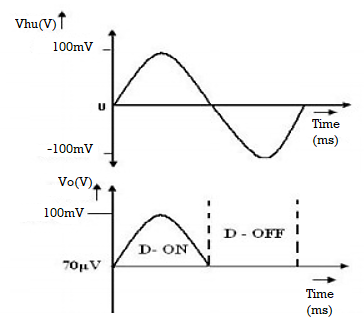
Fig 7 Input and Output of Precision Rectifier
The precision rectifier is another rectifier that converts AC to DC, but in a precision rectifier we use an op-amp to compensate for the voltage drop across the diode, that is why we are not losing the 0.6V or 0.7V voltage drop across the diode, also the circuit can be constructed to have some gain at the output of the amplifier as well.
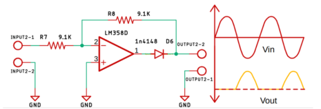
Fig 8 Half wave precision rectifier circuit.
The input and output waveform of the precision rectifier circuit, which is exactly equal to the input. That's because we are taking the feedback from the output of the diode and the op-amp compensates for any voltage drop across the diode. So, the diode behaves like an ideal diode.
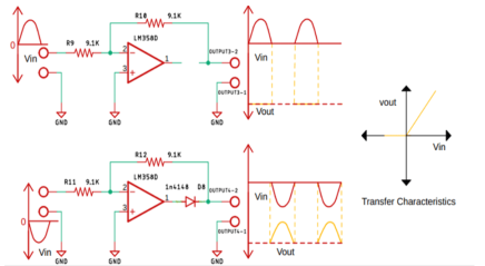
Fig 9 When positive and negative half cycle of input signal is applied to Op-amp
Full wave precision rectifier circuit
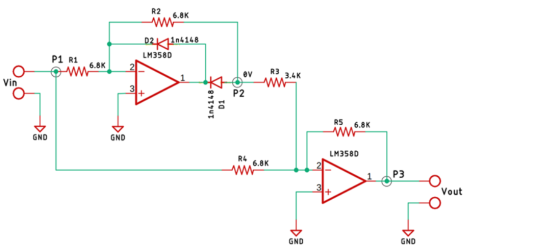
In full wave summing amplifier is added at the output. From the point, P1 to point P2 is the basic precision rectifier circuit and the diode is so configured that we get a negative voltage at the output.
From the point, P2 to point P3 is the summing amplifier, the output from the precision rectifier is fed to the summing amplifier through the resistor R3.
The input from the point P1 is also fed to the summing amplifier with the help of the resistor R4, the resistors R4 and R5 are responsible for setting the gain of the op-amp to 1X.
Since the output from the Point P2 is fed directly to the summing amplifier with the gain of 2X, that means the output voltage will be 2-times the input voltage. The output is obtained at P3.
Key takeaway
The precision diode operates in first quadrant when Vi>0 and V0>0. The precision diode operates in third quadrant when diode is connected in reverse bias
Astable Multivibrator
These multivibrators are termed as “Free Running” multivibrators, and they have only quasi stable states as seen earlier in introduction. The circuit diagram of astable multivibrator using Operational amplifier is shown below
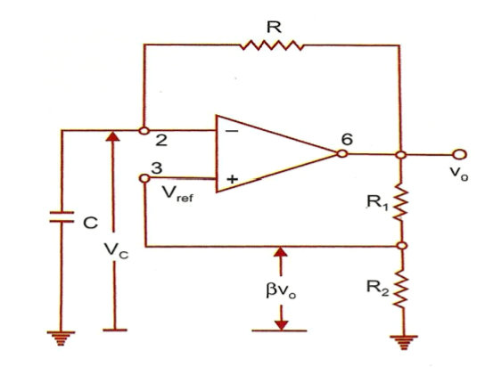
The circuit as simple and resembles like OP AMP Schmitt trigger circuit. One end of a capacitor C and a resistor R are connected to the inverting terminal. The other end of the resistor is connected to the output terminal and that of capacitor is connected to ground terminal. This capacitor C and feedback resistor R decide the period for oscillation of the multivibrator. A resistor R1 is connected between the output terminal and non-inverting terminal and another resistor R2 is connected between non-inverting terminal and ground terminals. If the output voltage is considered as Vo, then the voltage tapped between R2 shall be a reference voltage applied to the non-inverting terminal with amplitude of βVo where β is feedback factor for comparison.
Working
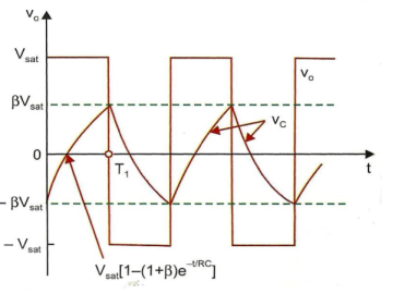
At Time 0: At time 0, assume the output transits from -Vsat to +Vsat. Since the output is +Vsat at time 0, reference voltage +βVo and capacitor voltage is -βVo.
From Time 0 to Time T1: Since reference is at +βVo, the inverting terminal is also at +βVo due to virtual ground. Now the capacitor tries to charge till the output voltage +Vo. It reaches +βVo and tries to charge more, then the inverting terminal go beyond reference voltage +βVo after time constant RC.
At Time T1: At time T1, since the inverting terminal goes little above than reference voltage +βVo, the output transits from +Vsat to -Vsat. Now capacitor voltage remains at +βVo. The reference voltage at non-inverting terminal is at -βVo. The time T1 is decided by RC (time constant) factor.
After Time T1: Since reference is at -βVo, the inverting terminal is also at -βVo due to virtual ground. Now the capacitor tries to charge till the output voltage -Vo. It tries to reach -βVo and tries to charge more, then the inverting terminal go beyond reference voltage -βVo after time RC (time constant). Now again whatever happened at time 0 happens again. These 3 steps repeat periodically till power is available for the circuit.
Circuit Analysis

Where VC is capacitor voltage, Vinitial and Vfinal are capacitors’ initial and final charging voltages respectively, t is the time function, RC is time constant where R and C are value of Resistor and capacitor attached to inverting terminal of the opamp. In this circuit


But as shown in the figure, T1 is only ON time and T is the total cycle time which is T1+T2 where T2 is considered =T1. Then T=2T1,


CASE 1
If  then
then  . Then


CASE 2
If  then
then  then
then


Thus when 
The frequency of oscillation of Astable multivibrator is

Monostable Multivibrators
These multivibrators are termed as “one-shot multivibrators” and they have only one stable state and other is quasi-stable state induced by single external trigger as seen earlier in introduction. The circuit diagram of monostable multivibrator using Operational amplifier is shown below
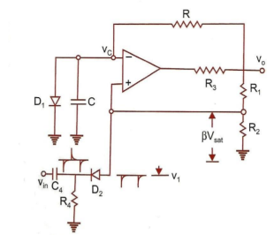
Fig 10.
The circuit as simple and resembles like OP AMP Schmitt trigger circuit. One end of a capacitor C and a resistor R are connected to the inverting terminal. The other end of the resistor is connected to the output terminal and that of capacitor is connected to ground terminal. A diode D1 is connected parallel to the capacitor C. This capacitor C and feedback resistor R decide the period for T of the multivibrator. A resistor R1 is connected between the output terminal and non-inverting terminal and another resistor R2 is connected between non-inverting terminal and ground terminals. If the output voltage is considered as Vo, then the voltage tapped between R2 shall be a reference voltage applied to the non-inverting terminal with amplitude of βVo where β is feedback factor for comparison. A pulse trigger circuit consisting of diode D2 and a differentiator circuit connected to pulse generator of negative pulse width Tp. The anode of the diode D2 is connected to non-inverting terminal.
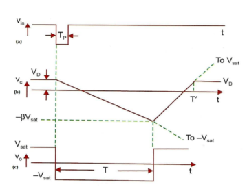
Fig. 11
Waveform a shows the pulse trigger waveform whose trigger pulse width is TP, waveform b shows voltage output VC across capacitor C and waveform c shows the monostable output Vo of quasi-stable state of time T. Before pulse trigger: At time before pulse trigger, assume the output is at +Vsat. Since the output is at +Vsat, then reference voltage is at +βVo and so capacitor voltage VC tries to charge towards +Vsat. Due to this the diode D1 gets forward biased when inverting terminal is positive, and the diode D1 starts conducting beyond 0.7V (Approximate cut-in voltage of Silicon diode). Thus the diode D1 conducts and provides a short path beyond 0.7V, and hence the capacitor C which is parallel can charge upto 0.7V only. So now the capacitor voltage VC is 0.7V.This voltage is shown as VD in the fig waveform (b). At time of pulse trigger: As shown in fig. Waveform (a & b), a negative pulse trigger is applied at non-inverting terminal and its amplitude being –Vin. Hence at the non-inverting terminal, pulse voltage –Vin and reference voltage +βVsat exists. The total voltage is (+βVsat –Vin). The amplitude of this voltage is less than 0.7V due to existence of diode D2 which is forward biased (ON) due to –ive trigger pulse (Cathode of the diode D2 is negative due to -Vin and anode is positive due to +βVsat). Now non-inverting terminal acts as reference terminal of an inverting comparator. At this point inverting terminal is at 0.7V and non-inverting reference voltage is below 0.7V. Hence inverting terminal is more than reference voltage at non-inverting terminal and the output transits from +Vsat to –Vsat as shown in fig. Waveform (c). That is output transited from stable high state to low state. The capacitor voltage VC is at 0.7V and output is at –Vsat. Hence the capacitor C starts charging towards -Vsat through the resistor R. The non-inverting terminal reference voltage is less than 0.7V.
At Time AFTER pulse trigger:
When pulse trigger ends after time TP, it becomes positive. So the cathode of diode D2 is at positive voltage and anode is at –βVsat. Thus the diode D2 is in reverse bias condition (OFF). Due to this the non-inverting voltage is affected only by reference voltage across resistor R2 which is -βVsat. Now reference voltage is at –βVsat and the charging capacitor is charging towards –Vsat. But when capacitor voltage VC reaches just above –βVsat, output transits from -Vsat to +Vsat (Inverting terminal voltage VC is more than reference voltage at non-inverting terminal). This transition happens at time T from start of pulse trigger where T is decided by RC time constant. That is capacitor C took time period of T for charging from VD to –βVsat which is through resistor R. The output stays at a quasi-stable state for a time period of T.
After Time T
Now output voltage Vo is at +Vsat and reference voltage at non-inverting terminal is at +βVsat. The capacitor starts charging from –βVsat to +Vsat. But when the capacitor voltage VC increases more than VD, diode D1 is forward biased and starts conducting. Hence the capacitor voltage VC cannot charge beyond VD. The waveform is shown in fig.waveform (a). As seen initially, now the amplitude at inverting terminal is VD due to charge of capacitor, non-inverting terminal voltage is at +βVsat. The output is a negative pulse voltage whose time period is T. This negative pulse was generated due to an external negative trigger (one-shot trigger). The output transit from a stable high state to a low quasi-stable state time T and then to a stable high state. This is a monostable waveform because it has one stable state and a quasi-stable state.
Analysis


But as shown in the figure, T1 is time period of Monostable multivibrator, it is considered as T Then T=T1,

If Vsat>>VD then VD / Vsat becomes negligible and R1=R2, then =0.5


The frequency of oscillation of monostable multivibrator is (if R1=R2)


Bistable Multivibrator
This is easy to use an operational amplifier as a bistable multivibrator. An incoming waveform is converted into short pulses and these are used to trigger the operational amplifier to change between its two saturation states. To prevent small levels of noise triggering the circuit, hysteresis is introduced into the circuit, the level being dependent upon the application required. The operational amplifier bistable multivibrator uses just five components, the operational amplifier, a capacitor and three resistors.
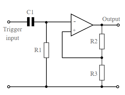
Fig 12 Simple bistable multivibrator circuit
The bistable circuit has two stable states. These are the positive and negative saturation voltages of the operational amplifier operating with the given supply voltages. The circuit can then be switched between them by applying pulses. A negative going pulse will switch the circuit into the positive saturation voltage, and a positive going pulse will switch it into the negative state.
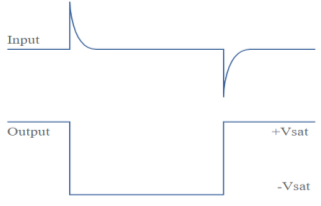
Fig 13 Waveforms for the bistable multivibrator circuit
It is very easy to calculate the points at which the circuit will trigger. The positive going pulses need to be greater than Vo-Sat through the potential divider, i.e. -Vsat x R3 / (R2 + R3), and similarly the negative going pulses will need to be greater than +Vsat through the potential divider, i.e. +Vsat x R3 / (R2 + R3). If they are not sufficiently large then the bistable will not change state.
When requiring a switching circuit, comparators are normally better than op amps as they do not exhibit the tendency that some op amps have to latch up. Also, comparators are much faster. That said, for some applications an op amp can work well enough.
- The Sample and Hold circuit are an electronic circuit which creates the samples of voltage given to it as input, and after that, it holds these samples for the definite time. The time during which sample and hold circuit generates the sample of the input signal is called sampling time.
- Similarly, the time duration of the circuit during which it holds the sampled value is called holding time.
- Sampling time is generally between 1µs to 14 µs while the holding time can assume any value as required in the application.
- It will not be wrong to say that capacitor is the heart of sample and hold circuit.
- This is because the capacitor present in it charges to its peak value when the switch is opened, i.e during sampling and holds the sampled voltage when the switch is closed.
Need for Sample and Hold Circuits
If the input analog voltage of an ADC changes more than ±1/2 LSB, then there is a severe chance that the output digital value is an error. For the ADC to produce accurate results, the input analog voltage should be held constant for the duration of the conversion.
It is based on a sampling command and holds the output value at its output until the next sampling command is arrived.
The following image shows the input and output of a typical Sample and Hold Circuit.
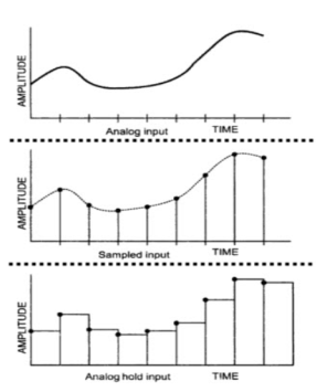
Fig 14 Input and output of S/H circuit
This sample and hold circuit consist of two basic components:
- Analog Switch
- Holding Capacitor
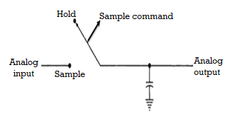
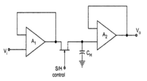
Fig 15 Open loop s/h circuit
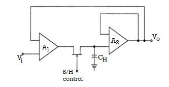
Fig 16 Closed loop s/h circuit
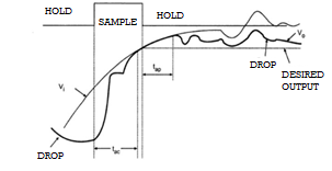
Fig 17 S/H characteristics
Acquisition Time (tac)
The time required for the charge in the holding capacitor to rise up to a level that is close to the input voltage during the sampling is called acquisition time. It is affected by three factors:
- The RC Time Constant
- The Slew-Rate of the Op-Amp
- The maximum output current of the Op-Amp
Aperture Time (tap)
The time delay between the initiation of VO tracking the Vi and the initiation of the hold command is called the Aperture Time. This delay is usually due to the propagation delays through the driver and the switch circuits.
For a precise timing operation, the hold command must be initiated in advance by an amount of aperture time.
Aperture Uncertainty (∆ tap)
The Aperture time will not be the same for all the sample and will vary from sample to sample. This uncertainty is called Aperture Uncertainty. This will severely affect the advancing of the hold command.
Hold Mode Settling Time (ts)
The hold mode settling time is the time taken by the output VO to settle within the specified error band (usually 1%, 0.1% or 0.01%) after the application of hold command.
Hold Step
During the switching from sample mode to hold mode, there might an unwanted transfer of charge between the switch and the holding capacitor (mainly due to the parasitic capacitances). This will affect the capacitor voltage as well as the output voltage. This change in the output voltage from the desired voltage is called Hold Step.
Feedthrough
Again, the parasitic capacitances in the switch may cause AC coupling between VO and Vi in hold mode. As a result, the output voltage may vary with changes in the input voltage and this is referred to as feedthrough.
Droop
Voltage Droop is a phenomenon where the voltage across the holding capacitor drops down due to leakage currents.
Advantages
- The main and important advantage of a typical SH Circuit is to aid an Analog to Digital Conversion process by holding the sampled analog input voltage.
- In multichannel ADCs, where synchronization between different channels is important, an SH circuit can help by sampling analog signals from all the channels at the same time.
- In multiplexed circuits, the crosstalk can be reduced with an SH circuit.
Key takeaways
They are used in
- Analog to Digital Converter Circuits (ADC)
- Digital Interface Circuits
- Operational Amplifiers
- Analog De-multiplexers
- Data distribution systems
- Storage of outputs of multiplexers
- Pulse Modulation Systems
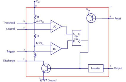
Fig 18 IC 555 Timer
For IC555 timer working as a flip flop or as a multi-vibrator, it has a particular set of configurations. Some of the major features include:
- It operates from a wide range of power ranging from +5 Volts to +18 Volts supply voltage.
- Sinking or sourcing 200 mA of load current.
- The external components should be selected properly so that the timing intervals can be made into several minutes along with the frequencies exceeding several hundred kilohertz.
- The output of a 555 timer can drive a transistor-transistor logic (TTL) due to its high current output.
- It has a temperature stability of 50 parts per million (ppm) per degree Celsius change in temperature which is equivalent to 0.005 %/ °C.
- The duty cycle of the timer is adjustable.
- Also, the maximum power dissipation per package is 600 mW and its trigger and reset inputs has logic compatibility.
Applications
The 555 generally operates in 3 modes:
- A-stable
- Mono-stable
- Bi-stable modes.
Astable mode
This means there will be no stable level at the output. So, the output will be swinging between high and low. This character of unstable output is used as a clock or square wave output for many applications.
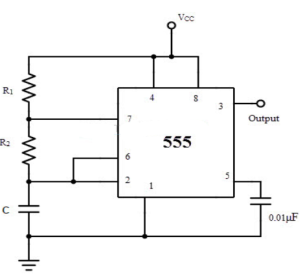
Fig 19 Astable Multivibrator
It is self-triggered multivibrator as pin 2 and 6 are connected. The supply is given through pin 8 and the output is obtained through pin 3. The timer will be reset if a low signal is given to pin 4. The capacitor is connected across pin 5 so that the external noise or any dc level are filtered. The resistor pair R1 and R2 form a circuit for determining the width of the output pulse.
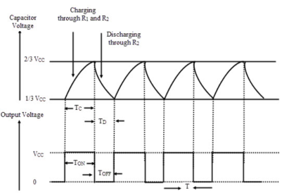
Fig 20 Capacitor and Output voltage waveform
During charging the capacitor charges through R1 and R2 and voltage across capacitor rises exponentially and during discharging the capacitor discharges through R2 and voltage falls exponentially. The output is obtained across pin 3.
The time for which capacitor charges from 1/3VCC to 2/3VCC is equal to the time the output is high which is given by
tc= 0.69(R1+R2) C
The discharging time from 2/3Vcc to 1/3VCC is given as
td= 0.69 R2C
The total period of output waveform is given by
T = tc+ td = 0.69(R1+2R2) C
The frequency of oscillations is given by
f0 =  =
= 
The duty cycle is defined as the ratio of the charging time of capacitor at which the output is high to the total time period.
%duty cycle =  x 100
x 100
Applications of Astable Multivibrator
Square wave Oscillator: The astable multivibrator shown in the figure below [Ref.1] can be used to generate square wave oscillations. The diode is connected across RB and the diode and capacitor are charged through RA to a voltage of 2/3 of VCC. The capacitor discharges through RB and Q1. The discharging of capacitor when reaches 1/3VCC the discharging stops.
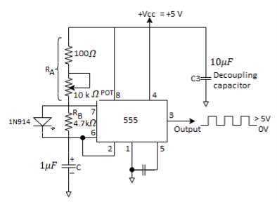
Fig 21 Astable multivibrator as square wave oscillator
Free-Running Ramp Generator
The circuit diagram is shown below [Ref.1]. The transistor Q1 is turned on by the comparator 1 when voltage across capacitor is 2/3Vcc. The capacitor C discharges through Q1. When capacitor discharges the voltage across C is 1/3Vcc, comparator 2 turns off Q1. The time period is given as
T = VCCC/3IC
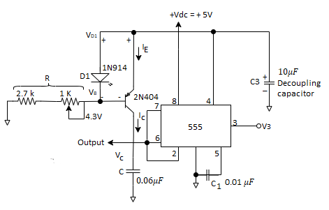
Fig 22 Free Running Ramp generator circuit
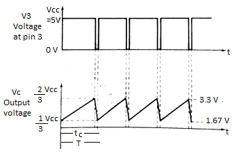
Fig 23 Output waveform
IC = (VCC-VBE)/R
The free running frequency of ramp generator is given by
f0 = 3IC/VCCC
The output waveform is shown in above figure.
Mono-stable mode
This configuration consists of one stable and one unstable state. The stable state can be chosen either high or low by the user.
If the stable output is set at high (1), the output of the timer is high (1). At the application of an interrupt, the timer output turns low (0). Since the low state is unstable it goes to high (1) automatically after the interrupt passes. The monostable multivibrator using IC555 is shown below.
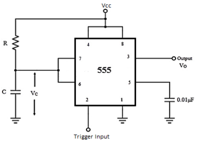
Fig 24 Monostable multivibrator using 555
The output is taken through pin 3. The supply is connected to pin 8. A small capacitor is connected to filter noise. The working is shown below in figure and explained as well.
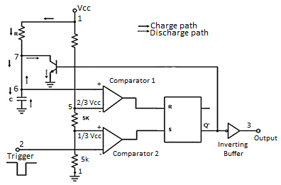
Fig 25 555 connected as monostable multivibrator
The discharge transistor will go to saturation when the F/F is reset. The discharge of C takes place through drain of CMOS. During negative pulse comparator 2 compares the pulse with reference voltage of 1/3 Vcc and output is low until the input becomes greater than the reference voltage. The output of F/F is set high when the output goes below 1/3Vcc. The output at pin 3 is high.
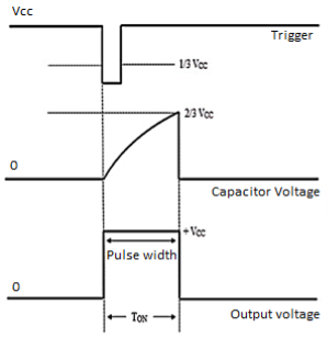
Fig 26 Input and Output waveform
When the C discharges the transistor is off and the voltage decays exponentially. This is input to the comparator 1 with reference voltage 2/3Vcc. The output is still high obtained at pin 3. The output of comparator is high when the threshold voltage becomes more than the reference voltage. Due to this the F/F is reset and output goes to zero. When the output is low the capacitor discharges completely and the transistor goes into saturation.
Pulse width
The voltage across C is Vc = Vcc (1-e-t/RC)
When voltage across capacitor is 2/3Vcc
2/3Vcc = Vcc (1-e-t/RC)
e-t/RC= 1/3
Taking log of both sides and solving we get
t= 1.098RC
The pulse width of rectangular pulse is 1.1RC (approx.)
Application of Monostable Multivibrator
Frequency Divider
The monostable multivibrator can be used as frequency divider by adjusting the time interval off charging. The charging time is made larger than the period of input pulse the device acts as divide-by-2 network. By proper selection of R and C the timing interval can be controlled. The waveform is shown below.
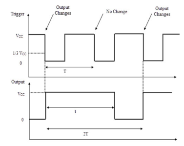
Fig 27 Divide-by-2 circuit waveform
When negative input pulse is applied the output goes high and will remain high irrespective of any other input pulse application as the timing interval s greater than the time period of trigger pulse. The circuit is triggered for every alternate negative going pulse.
Pulse Stretcher
This application makes use of the fact that output pulse width of monostable multivibrator is larger than the negative pulse width of trigger pulse. The output of monostable multivibrator is the stretched form of the input pulse. The pulse stretcher is shown below.
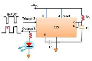
Fig 28 Pulse Stretcher
Example-1
An Astable 555 Oscillator is constructed using the following components, R1 = 1kΩ, R2 = 2kΩ and capacitor C = 10uF. Calculate the output frequency from the 555 oscillator and the duty cycle of the output waveform.
t1 – capacitor charge “ON” time is calculated as:
t1 = 0.693(R1 + R2). C
= 0.693(1000 +2000) x 10 x 10 -6 = 0.021 s= 0.21 msec
t2 – capacitor discharge “OFF” time is calculated as:
t2 = 0.693 R2. C
= 0.693 X 2000 x 10 x 10 -6 = 14ms
Total periodic time (T) is therefore calculated as:
T = t1 + t2 = 21 ms + 14 ms = 35 ms.
The output frequency, ƒ is therefore given as:
f = 1/T = 1/35ms = 28.6 Hz
Giving a duty cycle value of:
Duty Cycle = R1 + R2 / (R1 + 2 R2) = 1000 + 2000/ (1000 + 2 x 2000) = 60%
Key takeaways
S.No | Astable multivibrator | Monostable | Multivibrator |
1 | There are no stable states of output | There is only one stable state of the output | There are two stable states of the output. |
2 | Trigger input is not necessary for changing the state of the output | Trigger pulse is required for changing the state of output. | Trigger input is required for changing the state of output |
3 | Used as rectangular squarewave or ramp generator | Used as timer | Used as flip-flop |
4 | Number of quasi-stable state is 2. | Number of quasi-stable state is 1. | No quasi stable state. |
5 | Time for the two quasi stable states depends on RC time constant. The tow quasi stable states can have different intervals. | Time for the quasi table states depends on RC time constant | No quasi stable state. |
Key takeaway
They can be used as frequency divider, PWM, SR F/F, missing pulse detection etc.
A phase-locked loop consists of a phase detector and a voltage-controlled oscillator. The output of the phase detector is the input of the voltage-controlled oscillator (VCO) and the output of the VCO is connected to one of the inputs of a phase detector which is shown below in the basic block diagram. When these two devices are feed to each other the loop forms.
A basic phase locked loop, PLL, consists of three basic elements:
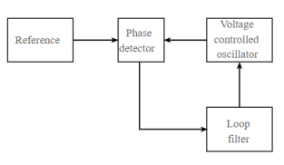
Fig 29 Block Diagram of PLL
- Phase comparator / detector: As the name implies, this circuit block within the PLL compares the phase of two signals and generates a voltage according to the phase difference between the two signals.
- Voltage controlled oscillator, VCO: The voltage-controlled oscillator is the circuit block that generates the radio frequency signal that is normally considered as the output of the loop. Its frequency can be controlled over the operational frequency band required for the loop.
- Loop filter: This filter is used to filter the output from the phase comparator in the phase locked loop, PLL. It is used to remove any components of the signals of which the phase is being compared from the VCO line, i.e. the reference and VCO input. It also governs many of the characteristics of the loop including the loop stability, speed of lock, etc.
Operation
The diagram for a basic phase locked loop shows the three main element of the PLL: phase detector, voltage- controlled oscillator and the loop filter.
In the basic PLL, reference signal and the signal from the voltage- controlled oscillator are connected to the two input ports of the phase detector.
The output from the phase detector is passed to the loop filter and then filtered signal is applied to the voltage- controlled oscillator.
The Voltage Controlled Oscillator, VCO, within the PLL produces a signal which enters the phase detector. The phase of the signals from the VCO and the incoming reference signal are compared and a resulting difference or error voltage is produced. This corresponds to the phase difference between the two signals.
The error signal from the phase detector passes through a low pass filter which governs many of the properties of the loop and removes any high frequency elements on the signal.
Once through the filter the error signal is applied to the control terminal of the VCO as its tuning voltage. The sense of any change in this voltage is such that it tries to reduce the phase difference and hence the frequency between the two signals.
Initially the loop will be out of lock, and the error voltage will pull the frequency of the VCO towards that of the reference, until it cannot reduce the error any further and the loop is locked.
When the PLL, phase locked loop, is in lock a steady state error voltage is produced. By using an amplifier between the phase detector and the VCO, the actual error between the signals can be reduced to very small levels.
However, some voltage must always be present at the control terminal of the VCO as this is what puts onto the correct frequency.
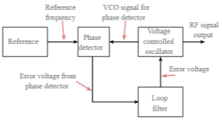
Fig 30 PLL showing voltages
The fact that a steady error voltage is present means that the phase difference between the reference signal and the VCO is not changing. As the phase between these two signals is not changing means that the two signals are on exactly the same frequency.
Key takeaways
The phase locked loop has three main elements: phase detector, voltage- controlled oscillator and the loop filter. When the PLL, phase locked loop, is in lock a steady state error voltage is produced. By using an amplifier between the phase detector and the VCO, the actual error between the signals can be reduced to very small levels.
References:
1. David A. Bell, ‘Op-amp & Linear ICs’, Oxford, 2013.
2. D. Roy Choudhary, Sheil B. Jani, ‘Linear Integrated Circuits’, II edition, New Age, 2003.
3. Ramakant A. Gayakward, ‘Op-amps and Linear Integrated Circuits’, IV edition, Pearson Education, 2003 / PHI. 2000.
4. N. C. Goyal and Khetan ‘A Monograph on Electronics Design Principals’, Khanna Publications
5. Sergio Franco, “Design with Operational Amplifiers and Analog Integrated Circuits”, McGraw Hill.