Unit - 4
Design of DC Power Supply
Half wave rectification
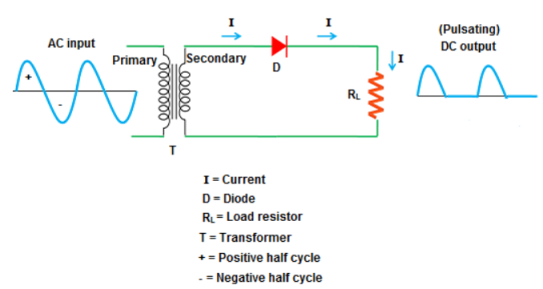
- It is the simplest form of the rectifier. Here, a single diode is used.
- It consists of an AC source, transformer (step-down), diode, and resistor (load).
- The diode is placed between the transformer and resistor (load).
Operation:
- It allows only half cycle and blocks the other half cycle.
- When it allows positive half cycles and blocks negative half cycles, it is called a positive half wave rectifier. The output DC current or DC signal produced by a positive half wave rectifier is a series of positive half cycles or positive sinusoidal pulses.
- When it allows electric current during the negative half-cycle of input AC signal and blocks electric current during the positive half-cycle of the input AC signal.
- A negative half wave rectifier produces a series of negative sinusoidal pulses.
- For an ideal diode, the positive half cycle or negative half cycle at the output is exactly same.
Characteristics of half wave rectifier
Ripple factor
The ripple factor is given as

Finally, we get
γ = 1.21
Hence, the DC voltage is 121% of the DC magnitude.
DC current
The DC current is given by,

Where,
Imax = maximum DC load current
Output DC voltage (VDC)
The output DC voltage is given by,

Where, VSmax = Maximum secondary voltage
Rectifier efficiency
It is defined as the ratio of output DC power to the input AC power.
The rectifier efficiency of a half wave rectifier is 40.6%
Root mean square (RMS)
The root mean square (RMS) value of load current in a half wave rectifier is

The root mean square (RMS) value of output load voltage in a half wave rectifier is

Form factor
It is defined as the ratio of RMS value to the DC value given by,
F.F = RMS value / DC value
The form factor of a half wave rectifier is F.F = 1.57
Advantages:
- Very few components are used. So, the cost is very low.
- Easy to construct
Disadvantages:
- Loss of power
- Pulsating direct current
- Produces low output voltage.
Key Takeaways:
- It allows only half cycle and blocks the other half cycle.
- When it allows positive half cycles and blocks negative half cycles, it is called a positive half wave rectifier and vice-versa.
Ques.
A half-wave rectifier is used to supply 50V d.c. To a resistive load of 800 Ω. The
diode has a resistance of 25 Ω. Calculate a.c. Voltage required.
Solution:
Output d.c. Voltage 
Diode resistance
Load resistance 
Let  be the maximum value of a.c voltage required


Hence a.c. Voltage of maximum value 162 V is required.
Full wave rectification
Types on the basis of construction:
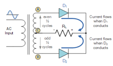
- Center-taped transformer
It consists of two power diodes connected to a single load resistance (RL) and each diode supply current to the load one by one. When point A of the transformer becomes positive, diode D1 conducts in the forward direction.
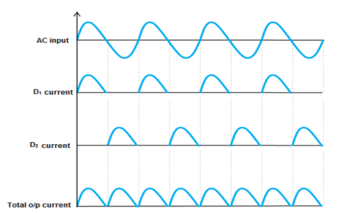
When point B becomes positive (for the negative half of the cycle) with respect to point C, diode D2 conducts and the current starts flowing through resistor R is in the same direction for both half-cycles.
As the output voltage across the resistor R is the sum of the two waveforms combined, this type of circuit is also called as a “bi-phase” circuit.
The spaces present between the frequency response of each half-wave developed by each diode is now being filled in by the other therefore, the average DC output voltage across the load resistor becomes double that of the single half-wave rectifier circuit.
2. Bridge Rectifier
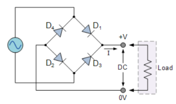
It uses four individual rectifying diodes which are connected in a closed loop called “bridge” configuration to produce the desired output.
It does not require a special centre tapped transformer, hence reducing its size and cost. The single secondary winding is connected one side to the diode bridge network and the other side to the load.
The four diodes D1 to D4 are arranged in “series pairs” and only two diodes conduct current during each half cycle.
During the positive half cycle, diodes D1 and D2 conduct in series while diodes D3 and D4 are reverse biased producing current through the load.
During the negative half cycle, diodes D3 and D4 conduct in series and diodes D1 and D2 are switched “OFF” as they become reverse biased producing current through the load.
During each half cycle the current flows through two diodes instead of just one. The ripple frequency is now twice the supply frequency.
Output Waveform:
Characteristics of full wave rectifier
Ripple factor
The ripple factor is given by

Finally, we get γ = 0.48
Rectifier efficiency
It is defined as the ratio of DC output power to the AC input power.
It can be mathematically written as
η = output PDC / input PAC
The rectifier efficiency of a full wave rectifier is 81.2%.
Peak inverse voltage (PIV)
It is the maximum voltage a diode can withstand in the reverse bias condition.
The peak inverse voltage (PIV) = 2Vsmax
DC output current
The current produced by D1 is Imax / π and the current produced by D2 is Imax / π.
So, the output current IDC = 2Imax / π
Where, Imax = maximum DC load current
DC output voltage
The DC output voltage appeared at the load resistor RL is given as
VDC = 2Vmax /π
Where,
Vmax = maximum secondary voltage
Root mean square (RMS) value of load current IRMS
The root mean square (RMS) value of load current in a full wave rectifier is

The root mean square (RMS) value of output load voltage in a full wave rectifier is

Form factor
It is the ratio of RMS value of current to the DC output current
F.F = RMS value of current / DC output current
The form factor of a full wave rectifier is F.F = 1.11
Advantages:
- High rectifier efficiency
- Low power loss
- Low ripples
- It has fewer ripples than the half wave rectifier.
Disadvantages:
- High cost
- The center tapped transformers are expensive and occupy a large space.
Key Takeaways:
- The process of converting the AC current into DC current is called rectification.
- When an additional wire is connected across the exact middle of the secondary winding of a transformer, it is known as a center tapped transformer.
- Bridge rectifier uses four individual rectifying diodes connected in a closed loop “bridge” configuration to produce the desired output.
Ques. A full-wave rectifier uses two diodes, the internal resistance of each diode may
be assumed constant at 20 Ω. The transformer r.m.s. Secondary voltage from center tap to each end of secondary is 50 V and load resistance is 980 Ω. Find: (i) the mean load current (ii) the r.m.s. Value of load current.
Solution:

Max a.c voltage 
Max. Load current 
(i) Mean load current 
Ii) RMS value of load current is

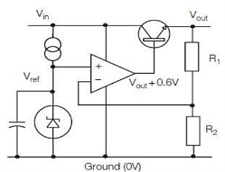
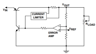
A simple voltage regulator is shown in Figure. This uses an op-amp to drive the base of a power transistor, to turn on the transistor and pass current from the input (Vin) to the output (Vout). The accuracy of the output voltage depends upon both the gain of the op-amp and the transistor, as well as the reference voltage Vref. This reference voltage is applied to the non-inverting input of the op-amp. A potential divider, comprising R1 and R2, applies a fraction of the output voltage to the inverting input of the op-amp. The output voltage is stable when the feedback voltage equals the reference voltage. The output voltage equals the reference voltage (developed across R1) plus the voltage drop across R2. The current through R2 is VREF/R1, therefore 

Integrated circuit voltage regulators are popular, because they have current limiting outputs and over-temperature shutdown circuits built into them. One such regulator is the LM317, which is produced by a number of manufacturers. This uses external resistors to set the output voltage and a typical circuit is shown in Figure. The reference voltage is a band-gap reference set at 1.25 V. Resistor R1 is usually set at 240kohm to give a nominal5 mA through the potential divider R1 and R2. This level of current over comes any errors due to small current leakage out of the LM317 reference terminal. The output voltage is given by the equations above. Capacitors C1 and C2 connected from the input and output terminals to ground are necessary to prevent oscillation.
There are two types of voltage regulators −
- Fixed voltage regulator
- Adjustable voltage regulator
Fixed voltage regulator
A fixed voltage regulator produces a fixed DC output voltage, which is either positive or negative. In other words, some fixed voltage regulators produce positive fixed DC voltage values, while others produce negative fixed DC voltage values.
78xx voltage regulator ICs produce positive fixed DC voltage values, whereas, 79xx voltage regulator ICs produce negative fixed DC voltage values.
The following points are to be noted while working with 78xx and 79xx voltage regulator ICs −
- “xx” corresponds to a two-digit number and represents the amount (magnitude) of voltage that voltage regulator IC produces.
- Both 78xx and 79xx voltage regulator ICs have 3 pins each and the third pin is used for collecting the output from them.
- The purpose of the first and second pins of these two types of ICs is different−
- The first and second pins of 78xx voltage regulator ICs are used for connecting the input and ground respectively.
- The first and second pins of 79xx voltage regulator ICs are used for connecting the ground and input respectively.
Adjustable voltage regulator
An adjustable voltage regulator produces a DC output voltage, which can be adjusted to any other value of certain voltage range. Hence, adjustable voltage regulator is also called as a variable voltage regulator.
The DC output voltage value of an adjustable voltage regulator can be either positive or negative.
Linear IC regulators contain built-in protection circuits which make them virtually immune to damage from either excessive load current or high operating temperature. The two protection circuits found in nearly all linear IC regulators are: Thermal Shutdown Current Limiting CHAIN OF COMMAND The thermal shutdown, current limiter, and voltage error amplifier make up three distinct and separate control loops that have a definite hierarchy (pecking order) which allows one to "override" the other. The order of command (and importance) of the loops is:
1) Thermal Limit (IC is regulating junction temperature/power dissipation)
2) Current Limit (IC is regulating load current)
3) Voltage Control (IC is regulating output voltage)
This hierarchy means that a linear regulator will normally try to operate in "constant voltage" mode, where the voltage error amplifier is regulating the output voltage to a fixed value. However, this assumes that both the load current and junction temperature are below their limit threshold values. If the load current increases to the limiting value, the current limiting circuitry will take control and force the load current to the set limiting value (overriding the voltage error amplifier). The voltage error amplifier can resume control only if the load current is reduced sufficiently to cause the current limiting circuits to release control.
Note that the thermal limiter can override both the current limit circuits and the voltage error amplifier. Thermal shutdown is detailed in the next section. It is important to understand that a regulator holds its output voltage fixed only when it is in constant voltage mode. In current limiting, the output voltage will be reduced as required to hold the load current at the set limiting value. In thermal limiting, the output voltage drops and the load current can be reduced to any value (including zero). No performance characteristic specifications apply when a part is operating in thermal shutdown mode.
THERMAL SHUTDOWN
The thermal shutdown circuitry in an IC prevents the junction temperature from rising high enough to damage the part (see Figure). This is accomplished by monitoring the die temperature and reducing internal power dissipation to hold the temperature at the limiting value (usually about 160°C).
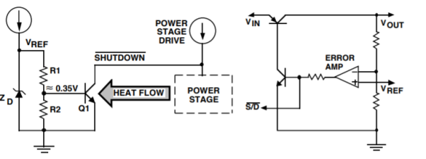
Circuit Operation: The temperature sensor (Q1) is located near the power transistor on the die, to assure very close thermal tracking. R1 and R2 hold the base of Q1 at about 0.35V, which corresponds to the turn-on VBE of Q1 at a temperature of about 160°C. As the die temperature increases, Q1 eventually reaches the turn-on threshold (about 160°C), and starts pulling current away from the current source which supplies drive to the power stage. In this way, the load current is reduced (or cut off entirely) which reduces the internal power dissipation of the regulator. In cases where thermal limiting occurs, both the output voltage and current will be reduced. When the output voltage drops below its nominal value, the error signal appearing at the voltage error amplifier will cause it to try and correct the regulator output voltage by driving its output high (and sourcing more current to the pass transistor). The thermal limit circuit can sink all of the current from the error amplifier output, and keep the regulator output voltage/current as low as needed to maintain the junction temperature at 160°C. As shown, the thermal limiter can "override" the voltage control loop when needed to prevent damage to the IC.
CURRENT LIMITING
The function of current limiting circuitry is to prevent damage to the IC when an overload is placed on the output of the regulator (the load impedance is too low). Without current limiting, the regulator would source excessive load current and destroy the pass transistor inside the part. To prevent this occurrence, the current limit circuit will override the voltage control loop, and cut down the drive to the pass transistor so that the maximum safe current level is not exceeded . There are two basic types of current limiting circuits most commonly used in linear regulators:
Constant Current Limiting
Voltage-Dependent Current Limiting
CONSTANT CURRENT LIMITING The maximum current that a linear regulator can supply to a load is specified on the data sheet. Many regulators (and most LDO regulators) specify only a single value of maximum current. This value is guaranteed for any input/output voltage within the maximum ratings for the part. For example, the LP2952 is guaranteed to source at least 250 mA without going into current limiting, as long as the output is in the 1.25V - 29V range and the input voltage is at least 0.8V above the output. In Figure, a simplified schematic diagram is shown of a circuit that will provide constant current limiting. This is a "discrete" design implementation (the circuitry used in an IC regulator may be slightly different).
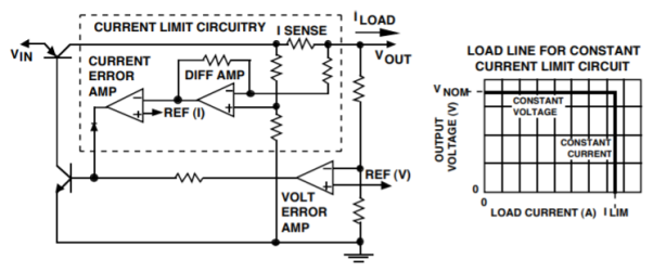
Circuit Operation:
The load current is sensed by the "I SENSE" resistor, which develops a voltage that is directly related to the current. This voltage is level shifted (and amplified) by the differential amplifier. The voltage at the output of the differential amplifier is a ground-referenced signal that is proportional to the load current. This "load current" signal coming from the differential amplifier is applied to the inverting input of the current limit error amplifier, while the non-inverting input is connected to a reference voltage.
The value of this reference voltage would be equal to the voltage at the output of the differential amplifier when the regulator is driving maximum current (at the current limit point). Note that as long as the load current is below the limit threshold, the output of the current error amplifier is high (and the voltage error amplifier keeps the regulator in constant voltage mode). When the load current reaches the limit threshold, the output of the current error amplifier drops low and starts sinking current away from the output of the voltage error amplifier (this puts the regulator in constant current mode). When current limiting occurs, the regulator output voltage will drop below its nominal value, which will be sensed by the voltage error amplifier as an undervoltage condition. The voltage error amplifier will drive its output high in an attempt to raise the output voltage, but the current error amplifier can sink all of the current coming from the voltage error amplifier.
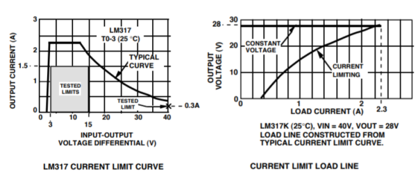
Like the thermal limiter, the current limiter overrides the voltage error amplifier to prevent damage to the IC. The load line shown in Figure above illustrates how the output voltage is held constant up to the point where the load current reaches the limit value, where the regulator crosses over into constant current mode. When operating in constant current mode, the IC regulates the load current to the "limit" value, which means the output voltage may be any value down to zero volts. It should be made clear that the thermal limiter can always override the current limiter, and can reduce the output voltage and current to any value necessary to maintain a junction temperature of about 160°C.
For example, if the LP2952 (which is rated for 250 mA) is shorted from the output to ground, a current will flow from the output which is greater than 250 mA but less than 530 mA (see "Current Limit specification on the data sheet). However, if the input voltage is high enough to generate sufficient power to activate the thermal limiter, that current will drop off as the LP2952 regulates its die temperature to about 160°C. Important: Current limit circuits are (by necessity) very high-speed circuits, and input bypass capacitors on the regulator are always recommended to prevent possible device failure due to interaction with the input source impedance.
VOLTAGE DEPENDENT (FOLDBACK) CURRENT LIMITING
Voltage regulators which are relatively high current (>1A) use a type of current limiting where the maximum allowable value of load current is dependent on the input-output voltage differential across the part. The reason this is required is due to a characteristic of all transistors called Safe Operating Area (SOA) that limits the amount of current a transistor can safely handle as the voltage increases.
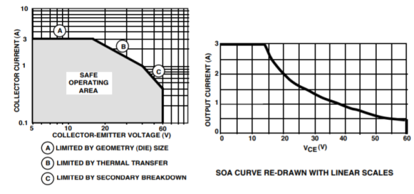
It is important to realize that the input-output voltage across a linear regulator is also the VCE across its pass transistor. This means the load current must be limited in accordance with the SOA curve of the regulator pass transistor.
CONSTANT CURRENT vs. FOLDBACK LIMITING
Constant current and foldback limiting have different characteristics that have the potential to cause some confusion. Assuming that the designer wished to test the current limiting, he could use an adjustable power resistor connected to the output of the regulator. As the resistance is adjusted to lower values (and the load current increases), the point will eventually be reached where current limiting occurs.
Constant Current Limiting: When current limiting first occurs, the output voltage is seen to drop from its nominal value as the regulator goes from constant voltage mode to constant current mode of operation. As the load resistance is decreased and current limiting occurs, the amount that the output voltage drops is directly proportional to the decrease in load resistance (because the load current is held constant). The drop in output voltage can be made to occur gradually, and the output voltage can be moved up and down by adjusting the load resistance. If the load resistance is increased above the point where the current limiter activated, the regulator will automatically go back into constant voltage mode (the output voltage will be in regulation).
Foldback Limiting: The action of a foldback limiting circuit is different, because it has some "hysteresis" built in to it. As the load resistance decreases to the point where limiting occurs, the output voltage can drop suddenly from the nominal voltage to a much lower value. Returning the load resistance back to the value where limiting started may not restore the output voltage to nominal (the load resistance may have to be increased to a higher value to allow the regulator to return to constant voltage operation). This apparent "hysteresis" is due to the shape of the "foldback" current limit curve.
The Switched mode power supply is abbreviated as SMPS is used to convert the regulated DC output voltage from unregulated DC or AC voltage. The basic block diagram showing the working of SMPS is represented below.
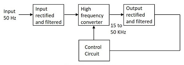
Input Unit
The rectifiers and the filters are fed with a 50Hz input supply. The capacitance value of the capacitor should be high as there can be fluctuations in the output. There is no need for any transformer for input supply as the rectifier and filter circuit combinations are used.
Switching Section
As there are various fluctuations at the output of the input unit Power transistors or MOSFETs are used for fast switching. They can be turned ON or OFF as per the need and the output from here is fed to the transformer present in this section.
Output Unit
The desired DC output is obtained by again passing the output from the switching section to the rectifier and filter unit. The regulated output voltage obtained from here is again fed as input to the control unit through a feedback circuit.
Control Unit
The control unit consists of many other small units functioning together as represented below.

The input to the control unit is fed to the sensor. The final output voltage is controlled by controlling the chopping frequency. This helps to maintain the final voltage level. This is achieved by comparing the error amplifier inputs. The input to the error amplifier is the signal from the sensor and one reference signal. The reference signal is nothing but the required output signal; the error amplifier compares the mentioned two signals and generates the required output voltage level accordingly. The PWM oscillator produces a standard PWM wave fixed frequency.
Types of SMPS
There are four main types of SMPS listed below
- DC to DC Converter
- AC to DC Converter
- Fly back Converter
- Forward Converter
Applications
There are many applications of SMPS. They are used in the motherboard of computers, mobile phone chargers, HVDC measurements, battery chargers, central power distribution, motor vehicles, consumer electronics, laptops, security systems, space stations, etc.
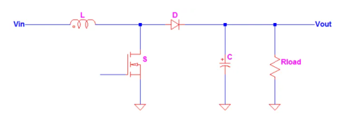
A typical Boost converter is shown below.
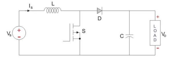
The input voltage source is connected to an inductor. The solid-state device which operates as a switch is connected across the source. The second switch used is a diode. The diode is connected to a capacitor, and the load and the two are connected in parallel as shown in the figure above.
The inductor connected to input source leads to a constant input current, and thus the Boost converter is seen as the constant current input source. And the load can be seen as a constant voltage source.
The controlled switch is turned on and off by using Pulse Width Modulation (PWM).
The Boost converter has two modes of operation. The first mode is when the switch is on and conducting.
Mode I: Switch is ON, Diode is OFF
The switch is ON and therefore represents a short circuit ideally offering zero resistance to the flow of current so when the switch is ON all the current will flow through the switch and back to the DC input source. Let us say the switch is on for a time TON and is off for a time TOFF. We define the time period, T, as
T = TON + T OFF
And the switching frequency
f switching = 1/T.
Let us now define another term, the duty cycle,
D = TON/T
Let us analyze the Boost converter in steady state operation for this mode using KVL.
Vin = VL
VL = L diL /dt = Vin
DiL/dt = ∆ iL/∆t = ∆iL/DT = Vin/L
Since the switch is closed for a time Ton = DT we can say that ∆t=DT
(∆ iL) closed= (Vin/L) DT
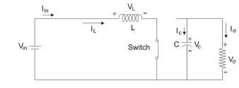
Analysis and waveforms at steady state
Let us analyze the Boost converter in steady state operation for this mode using KVL. Since the switch is closed for a time TON = DT we can say that Δt = DT.
While performing the analysis of the Boost converter, we have to keep in mind that
- The inductor current is continuous and this is made possible by selecting an appropriate value of L.
- The inductor current in steady state rises from a value with a positive slope to a maximum value during the ON state and then drops back down to the initial value with a negative slope. Therefore, the net change of the inductor current over anyone complete cycle is zero.
Mode II: Switch is OFF, Diode is ON
In this mode, the polarity of the inductor is reversed. The energy stored in the inductor is released and is ultimately dissipated in the load resistance, and this helps to maintain the flow of current in the same direction through the load and also step-up the output voltage as the inductor is now also acting as a source in conjunction with the input source. But for analysis, we keep the original conventions to analyze the circuit using KVL.
Let us now analyse the Boost converter in steady state operation for Mode II using KVL.
Vin = VL + Vo
VL = L diL/dt = Vin -VO
DiL/dt = ∆ iL/∆t = ∆ iL / (1-D) T = Vm-Vo/L
Since the switch is open for a time
TOFF = T – TON = T -DT = (1-D) T
We can say that
∆t = (1-D) T
(∆ iL) open = (Vin -Vo/L) (1-D) T
It is already established that the net change of the inductor current over any one complete cycle is zero
(∆ iL) closed + (∆ iL) open =0
(Vin – Vo) /L (1-D) T + (-Vo/L) DT =0
Vo /Vin = 1/ 1-D
Since the switch is open for a time
TOFF = T – TON = T – DT = (1-D) T
We can say that
∆t = (1-D) T
It is already established that the net change of the inductor current over any one complete cycle is zero.
(∆ iL) closed + (∆ iL) open =0
(Vin – Vo/L) (1-D) T + (-Vo/L) DT =0
Vo /Vin = 1/ 1-D
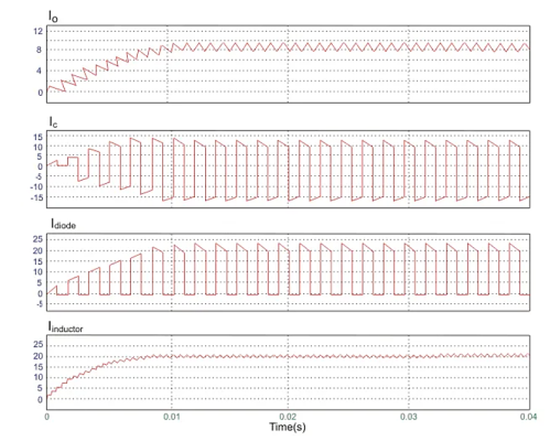
A circuit of a Boost converter and its waveforms are shown below. The inductance, L, is 20mH and the C is 100µF and the resistive load is 20Ω. The switching frequency is 1 kHz. The input voltage is 100V DC and the duty cycle is 0.5.
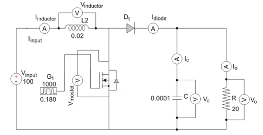
The voltage waveforms are as shown above and the current waveforms are as shown in the figure below.
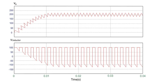
The voltage waveforms are as shown above and the current waveforms are as shown in the figure below.
Relation between duty ratio and average output voltage.
The inductor of the boost converter charges during Ton and discharges during Toff. The inductor current waveform is then resembled like Figure 2 below.
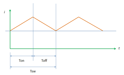
The figure is an inductor waveform of a continuous conduction mode boost converter. A boost converter by the way can operate in three modes; continuous conduction (CCM), discontinuous conduction (DCM) and boundary mode. For CCM the inductor current will not reach zero after every switching cycle. For DCM, the inductor current is reaching zero before the next Ton occur.
How to Calculate the Duty Cycle of Boost Converter – Analysis during Ton
During Ton, the switch S is on. The diode will be reversed biased and this
time the load is being supplied by the energy stored in the capacitor C. The inductor will charge. The flow of the current is from Vin to inductor L then to switch S. By KVL,

Then expressing VL
 -------------------------(1)
The voltage across inductor is also defined by below formula.

---------------------------------------(2)
Expressing the change in current di
 ---------------------------------------(3)
Substitute 1 to 3
 ----------------------------------------(4)
Then we will get rid of the variable dt by integrating the equation from 0 to Ton.

 ----------------------------------------------------(5)
How to Calculate the Duty Cycle of Boost Converter – Analysis during Toff
During Toff, the inductor reverses its polarity and the diode at this time will be forward biased and the load will be supplied by the energy in the inductor. The energy on the inductor will start to decay. The flow of current is from Vin to diode D then to the load. Applying KVL,

Expressing VL,
 ------------------------------------------(6)
Substituting [Eq. 6] to [Eq. 3] will result to
 ----------------------------------(7)
Then we will eliminate the variable dt through integration from Ton to T.
 ---------------------------------------(8)

Now go back to Figure 2, the magnitude of the inductor current during Ton and Toff is equal. Therefore, we can equate [Eq. 5] and [Eq. 8].


Then substitute Ton = DT

Then solving for the duty cycle, D

-----------------------------------------------------(9)
Eq. 9
Assuming ideal values (diode and switch voltage drops are zero)
 ----------------------------------------(10)
Output Voltage:
The relationship of voltage and current for an inductor is:

, or

For a constant rectangular pulse:

From this we can see that the current is a linear ramp, when the voltage is a constant pulse.
When the transistor switches on the current is:

 or
or
And when the transistor switches off the current is:

, or
 (Equation 1)
Where VD is the voltage drop across the diode, and VTrans is the voltage drop across the transistor. Note that the continuous/discontinuous boundary occurs when io is zero.
By equating through delta i, we can solve for Vout:


We can also solve for the duty cycle as follows,


If we neglect the voltage drops across the transistor and diode then:

So, it is clear that the output voltage is related directly to the duty cycle of the pulses.
Buck Boost Converter
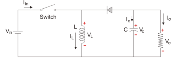
It is basically a DC-DC converter which has output either low or high than the input voltage value. It is combination of a step up (Buck) and step up (Boost) converter. These devices have a diode connected with inductor and a capacitor. The input is connected to a solid-state device. The diode acts as a switch. The circuit shown below is of a buck-boost converter.

Fig: Buck-Boost Converter
The diode is in the reverse direction to the source. The capacitor and diode are in parallel to load. We use pulse width modulation to turn the controlled switch ON and OFF. Normally time based PWM is used as frequency based is difficult in implementation. This operates in two modes
i) When switch is ON, Diode is OFF:
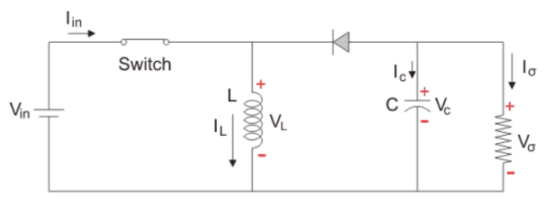
As seen from the above figure when the switch is ON it acts as a short circuit and hence, allows all the current to pass through it. In this condition the current flows through the switch and inductor and again to the input. The inductor stores energy at this time. When the switch is OFF the inductor reverses its polarity and then the current flows through the load and then diode and back to the inductor.
The total time period T = TON+TOFF
TON: ON time
TOFF: OFF time
The switching frequency fs= 1/T
In steady state Vin=VL
VL= L  = Vin
= Vin
Now duty cycle D= 
 =
= 
At end of ON state
 ILON =
  =
=  dt =
dt = 
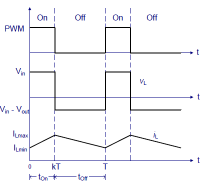
Ii) When switch is OFF, Diode is ON:
The circuit is shown below where the switch is in OFF state. The polarity of inductor is reversed. The current flows through the load resistance from the inductor and a step-up voltage is obtained at the output.
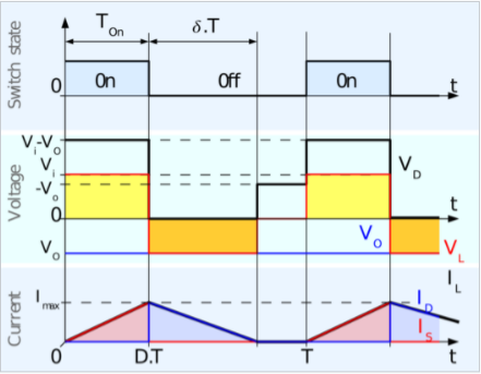
In this case VL=Vo
VL= L  = Vo
= Vo
 =
= 
TOFF= T-TON = T_DT = (1-D) T
 t= (1-D) T
 iL)open=
  (1-D) T
Solved Examples
Q1) A transistor dc chopper circuit (Buck converter) is supplied with power form an ideal battery of 100 V. The load voltage waveform consists of rectangular pulses of duration 1 ms in an overall cycle time of 2.5 ms. Calculate, for resistive load of 10 Ω. (a) The duty cycle γ. (b) The average value of the output voltage Vo. (c) The rms value of the output voltage Vorms. (d) The ripple factor RF. (e) The output dc power.
A1)
(a) 

(b) 


Q2) An 80 V battery supplies RL load through a DC chopper. The load has a freewheeling diode across it is composed of 0.4 H in series with 5Ω resistor. Load current, due to improper selection of frequency of chopping, varies widely between 9A and 10.2. (a) Find the average load voltage, current and the duty cycle of the chopper. (b) What is the operating frequency f ? (c) Find the ripple current to maximum current ratio.
A2)
(a) The average load voltage and current are

(a) The average load voltage and current are:


(b) To find the operating (chopping) frequency:
During the ON period, 
Assuming 

From eq (1)


But


Hence 
The maximum current  occurs at =1

Ripple current 

Q3) A DC Buck converter operates at frequency of 1 kHz from 100V DC source supplying a 10 Ω resistive load. The inductive component of the load is 50mH.For output average voltage of 50V volts, find: (a) The duty cycle (b) ton (c) The rms value of the output current (d) The average value of the output current (e) Imax and Imin (f) The input power (g) The peak-to-peak ripple current.
A3)
(a) 

(b) 

(c) 
(d) 
(e) 
(f)


(g)

A dc chopper in figure has a resistive load of and input voltage of V = 200 V. When chopper is ON, its voltage drop is 2 V and the chopping frequency is 1 kHz. If the duty cycle is 60%, determine Average output voltage RMS value of output voltage Effective input resistance of chopper Chopper efficiency.
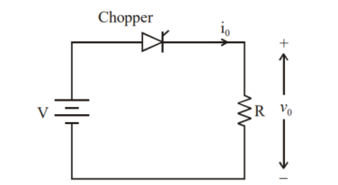
 Cho[[er voltage drop,
Average output voltage


RMS value of output voltage


Effective input resistance of chopper is


Output Power:


Input Power:


Chopper efficiency


Q) A chopper feeding on RL load is shown in figure, with V = 200 V, R = 5, L = 5 mH, f = 1 kHz, d = 0.5 and E = 0 V. Calculate – Maximum and minimum values of load current. – Average value of load current. – RMS load current. – Effective input resistance as seen by source. – RMS chopper current.
A)


Chopping period is 
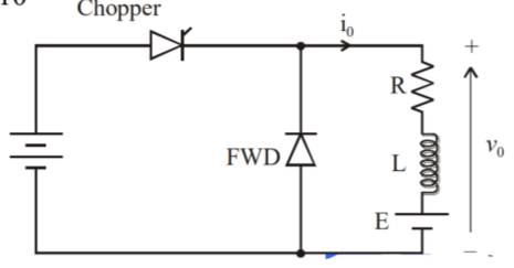
Maximum value of load current is given by


Minimum value of closing current is given by


Average value of load current is

For linear variations of current

RMS load current is given by


RMS chopper current is given by

Effective input resistance is

 Average source current


Therefore effective input resistance is

Q1) A Chopper circuit is operating on TRC at a frequency of 2 kHz on a 460 V supply. If the load voltage is 350 volts, calculate the conduction period of the thyristor in each cycle.
A1) 
Chopping period 

Output voltage 
Conduction period of thyristor


Q2) Input to the step up chopper is 200 V. The output required is 600 V. If the conducting time of thyristor is 200 µsec. Compute – Chopping frequency, – If the pulse width is halved for constant frequency of operation, find the new output voltage.
A2) 


Solving for T

Chopping frequency 
Pulse width is halved

Frequency is constant 

Output voltage 
Q3) A dc chopper has a resistive load of 20Ω and input voltage VS = 220V. When chopper is ON, its voltage drop is 1.5 volts and chopping frequency is 10 kHz. If the duty cycle is 80%, determine the average output voltage and the chopper on time.
A3)


 Voltage drop across chopper =1.5 volts
Average output voltage

 =0.80(220-1.5)=174.8 volts

Chopping period


Chopping ON time


Q4) In a dc chopper, the average load current is 30 Amps, chopping frequency is 250 Hz, supply voltage is 110 volts. Calculate the ON and OFF periods of the chopper if the load resistance is 2 ohms.
A4)

Chopping period 


Chopper ON period,

Chopper OFF period,


References:
1. David A. Bell, ‘Op-amp & Linear ICs’, Oxford, 2013.
2. D. Roy Choudhary, Sheil B. Jani, ‘Linear Integrated Circuits’, II edition, New Age, 2003.
3. Ramakant A. Gayakward, ‘Op-amps and Linear Integrated Circuits’, IV edition, Pearson Education, 2003 / PHI. 2000.
4. N. C. Goyal and Khetan ‘A Monograph on Electronics Design Principals’, Khanna Publications
5. Sergio Franco, “Design with Operational Amplifiers and Analog Integrated Circuits”, McGraw Hill.