Unit - 1
Introduction to Microcontrollers
Basically, a microcontroller is classified based on the following categories listed below
Based on Memory
Depending upon the type of memory it is classified as External memory microcontroller and Embedded Memory Microcontroller. For external memory microcontroller we need to provide external program memory as the microcontroller does not have any on chip memory. On the other hand, Embedded memory microcontroller has on chip program and data memory. These controllers have I/O ports, timer, interrupts and counters embedded on chip.
Based on Architecture
According to Von Neumann Architecture the storage of data and program has common memory. But there are separate memory units for program and data storage in Harvard Architecture. Also, it has separate buses for transfer of data and instructions.
Based on Bit Configuration
In case of 8-bit microcontroller it processes 8 bits of data at a time. It is employed for basic arithmetic and logical operations such as addition, subtraction, multiplication and division. For higher accuracy and performance 16-bit microcontrollers are used. For superior processing and speed control we use 32-bit microcontroller. For automatic controlling of appliances like computer and medical we use 32-bit MC.
Based on Instruction Set
The Complex Instruction Set Computer (CISC) allows the user to replace multiple simple instructions with a single simple instruction. The Reduced Instruction Set Computer (RISC) reduces the clock cycle per instructions by reducing the operational time.
Key takeaway
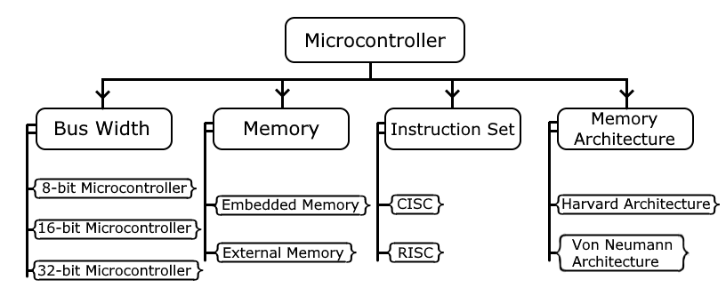
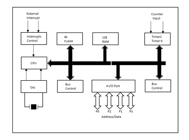
Figure 1. 8051 Architecture
Central Processor Unit (CPU)
The brain of any processing device of the microcontroller is the CPU. It monitors and controls all operations performed on these units. It reads program written in ROM memory, executes and does the expected task.
Interrupts
Interrupt is a subroutine call that interrupts the microcontrollers main operations or work and causes it to execute any other program, at the time of operation. It provides a mechanism to put on hold the ongoing operations, execute a subroutine and resume to another type of operation.
8051 has five interrupt sources:
- INTO
- TFO
- INT1
- TF1
- R1/T1
(INT0) ̅ and (INT1) ̅ are external interrupts negative edge triggered or low level triggered. When these interrupts are activated, the corresponding flags are set except for serial interrupt.
When the processor branches to ISR the interrupt flags are cleared. The external interrupts are timer and serial port interrupts.
Memory
They require memory to save as well as read so that the microcontroller performs specific operations of the task.
The memory which is used to store the program known as code memory or Program memory It is also known as ROM memory.
8051 data memory is used to storing data temporarily for operation known as RAM memory. It has 4K of code memory or program memory and 128 bytes of data memory of RAM.
BUS
A collection of wires that work as communication channel or medium for transfer of data. It consists of 8, 16 or more wires of microcontroller. Thus, they carry 8 bits or 16 bits of data simultaneously. There are two types of buses which are
Address Bus
Data Bus
Address Bus:
Microcontroller 8051 has a 16-bit address bus for transferring data. It addresses memory locations to transfer address from CPU to Memory. It has four addressing modes that are:
- Immediate addressing modes.
- Bank address (or) Register addressing mode.
- Direct Addressing mode.
- Register indirect addressing mode.
Data Bus: Microcontroller 8051 has 8 bits of data bus used to carry data for applications.
Oscillator
The 8051 microcontroller has an on-chip oscillator that acts as a clock source for CPU of microcontroller. The output pulses of the oscillator are stable. Therefore, it enables synchronized work for all the parts of Microcontroller system.
Input/output Port
To control the operation of machines microcontroller is used in embedded systems. To connect to other machines, devices or peripherals I/O interfacing ports is required. Microcontroller 8051 has 4 input and output ports to connect to other peripherals
Timers/Counters
8051 microcontroller has two 16-bit timers and counters. The counters are again divided into 8-bit register. Timers are used for measurement of time intervals to determine pulse width.
Block Diagram
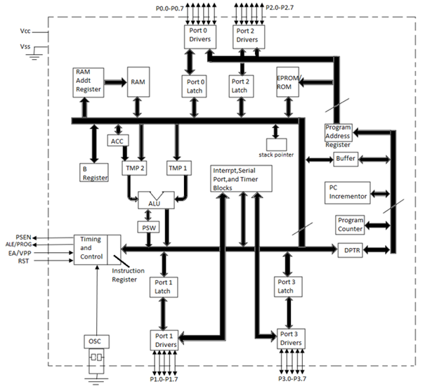
Figure 2. Block Diagram of 8051
ALU
ALU performs all arithmetic and logical functions.
Addition, subtraction with carry, and multiplication are categorized as arithmetic operations.
Logical AND, OR and exclusive OR (XOR) as logical operations.
Program Counter (PC)
A program counter is a 16-bit register that has no internal address. The program counter fetches the address of the next instruction to be executed from memory. The PC holds the address of next instruction residing in memory. When a command is encountered, it executes that instruction. PC increments and holds the address of the next instruction.
Registers
Registers are known as data storage devices. There are two registers namely Register A and Register B. Register A is used as an accumulator and Register B as general -purpose register. The output of mathematical and logical instructions are stored in these registers.
The operations of addition, subtraction, multiplication and division are performed by Register A. Register B is for multiplication and division which are carried by Register A. For data transfers between microcontroller and external memory Register A is involved.
8051 microcontrollers also have 7 Special Function Registers (SFRs). They are:
1. Serial Port Data Buffer (SBUF)
2. Timer/Counter Control (TCON)
3. Timer/Counter Mode Control (TMOD)
4. Serial Port Control (SCON)
5. Power Control (PCON)
6. Interrupt Priority (IP)
7. Interrupt Enable Control (IE)
4. Timers and Counters
In internal operations synchronization is achieved by clock circuits for generating clock pulses. During each clock pulse operations assure synchronization.
For oscillator formation XTAL1 and XTAL2 are used to form resonant network. It consists of four more pins.
1. EA: External enable
2. ALE: Address latch enable
3. PSEN: Program store enable and
4. RST: Reset.
Quartz crystal is used for generating periodic clock pulses.
5. Internal RAM and ROM
ROM
In 8051 a code of 4K memory is incorporated as on-chip ROM. ROM is a non-volatile memory that is its contents cannot be altered. They can address program memory and data memory which is a separate block of 64KB.
RAM
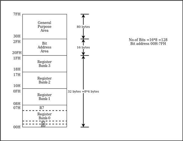
The internal RAM of 8051 microcontroller is composed of 128 bytes. It is a volatile memory because its contents is lost if power is switched off.
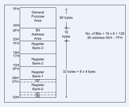
In internal RAM 128 bytes is divided into 32 working registers which constitute of 4 register banks (Bank 0-Bank 3), each bank consisting of 8 registers (R0 - R7). Internal RAM consists of 128 addressable bits.
6. Four General Purpose Parallel Input/Output Ports
It consists of four 8-bit input/output ports.
These are:
PORT P0: In absence of external memory present, this port acts as a general-purpose input/output port. In the presence of external memory, it operates as multiplexed address and data bus performing dual role.
PORT P1: This port is used for different interfacing activities. This 8-bit port is a normal I/O port and does not perform dual functions.
PORT P2: Port 2 is like PORT P0 which is used as general- purpose port if no external memory is present. However, in presence of external memory, it works in conjunction with PORT PO as an address bus. This is an 8-bit port which performs dual functions.
PORT P3: PORT P3 behaves as dedicated I/O port.
7. Interrupt Control
An interrupt is either an internal or external event where the microcontroller suspends for a certain time by obstructing the sequential flow of a program.
There are two ways of giving interrupts to a microcontroller
- Sending software instructions
- Sending hardware signals.
In interrupt mechanism 8051 keeps the normal program execution in “put on hold" mode and executes a subroutine program. After execution of subroutine it returns to normal program execution. This subroutine program is called an interrupt handler. A subroutine is executed when certain event occurs.
8051 is provided with 5 sources of interrupts are provided.
They are:
a) Two external interrupt sources connected through INT0 and INT1
b) Three external interrupt sources- serial port interrupt, Timer Flag 0 and Timer Flag 1.
8. Serial Data Communication
In serial data communication is established among computers by transmitting and receiving data bits in a serial connection network.
For holding data SBUF (Serial Port Data Buffer) register;
Manage data communication SCON (Serial Control) register
Managing data transfer rate PCON (Power Control) register
RXD and TXD establish serial network.
SBUF register has 2 parts
For storing the data to be transmitted use TXD pin
For receiving data from other source use RXD pin.
Serial data communication operates in four modes. They are serial data
1. Mode 0 (shift register mode)
2. Mode 1 (standard UART)
3. Mode 2 (multiprocessor mode)
4. Mode 3
9. PSW (Program Status Word)
Program Status Word or PSW is a hardware register a memory location which holds a program's information and monitors the status of the program this is currently being executed. It has a pointer which points towards the address of the next instruction to be executed.
The register has 3 fields namely instruction address field, condition code field and error status field. PSW is an internal register which keeps track of the computer at every instant.
There are7 flags in PSW. 4 are math flags and 3 are general purpose or user flags.
The Math flags are:
• Carry (c)
• Auxiliary carry (AC)
• Overflow (OV)
• Parity (P)
The General-purpose flags or User flags are:
• FO
• GFO
• GF 1
10. Data Pointer (DPTR)
DPTR is a 16-bit register. It consists of two 8-bit registers DPH and DPL. Separate addresses are assigned to each DPH and DPL. These 8-bit registers are used for storing memory addresses which can be accessed internal and external data/code.
11. Stack Pointer (SP)
A special area of data in memory. The stack pointer is an 8-bit register whose main function is to access the stack. It can take values in the range 00 H to FF H. SP acts as a pointer to points to an address at the top of the stack.
12. Data and Address Bus
A bus consists of group of wires to transfer data from one location to another within the system. Buses reduce the number of paths or cables needed to set up connection between components.
There are two kinds of buses - Data Bus and Address Bus
Data Bus: The purpose of data bus is to transfer data. It acts as a channel for data to travel.
Address Bus: The purpose of address bus is to transfer information but not data. The information tells from where within the components, the data should be sent to or received from.
Port Structure
8051 has four ports P0,P1,P2,P3. They are required for I/O operations.
32 pins are set for four ports P0,P1,P2,P3. Each port takes 8 pins.
All the ports are configured as input upon Reset
When zero is written to port it becomes output. To make it input 1 needs to be sent to the port.
Port 0:
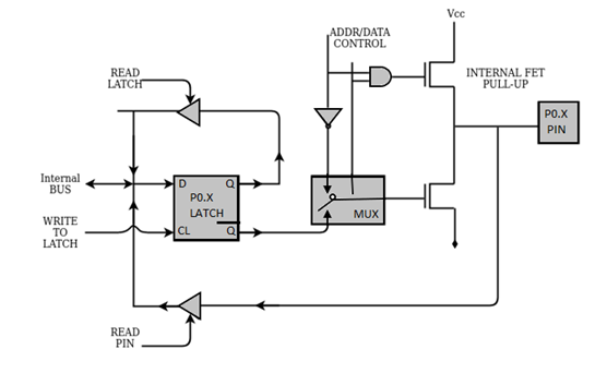
Fig 3. Port -0
When Port0 is used as input port 1 must be written to the corresponding zero latch that causes the output transistor to switch off and pin floats in high impedance state.
When configured as input port it provides two facilities:
Reads logic level on physical pin by asserting read pin signal.
Read contents of internal latch by asserting the read latch signal.
The latch is read for instruction read-modify-write type instruction.
It reads data from the port modifies and writes to the port.
When Port0 is configured as output the latch pins that are programmed to 0 will cause the lower FET to turn ON and pin is grounded.
If 1 is written to the latch pin FET will turn OFF and pin is pulled HIGH by external pull-up resistor.
Port 1:

Figure 4. Port 1 circuit
When port 1 is used as in input port ‘1’ must be written to the corresponding port1 latch bit. This causes the lower FET to turn off.
The pin and the input buffer are pulled to logic HIGH by internal pull load.
This port is called quasi-bidirectional port because its output is pulled high with pull up resistor.
When port 1 is used as an output port, the latch pins that are programmed to 0, will cause the lower FET turn on the internal pull to turn off and input is logic 0.
If 1 is written onto the latch, then it will drive the input of external circuit high through pull up. The lower FET turns off.
Port 2:
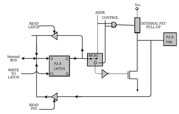
Figure 5. Port 2 circuit
When Port2 is used as an input port 1 must be written to the corresponding latch bit. This cause the FET turn off. The pin and input to pin buffer are pulled to logic high by internal pull up load.
Port 2 is called as “quasi-bidirectional port” as its output is pull up resistors.
When port2 is used as output port the latch pins that are programmed to 0, will cause the lower FET to turn off and input to the circuit logic 0.
If “1” is written onto latch pin, then it will drive the input of external circuit high through pull-up. The lower FET turns off.
Port 3:
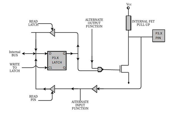
Figure 6. Port 3 circuit
When port3 is used as input port 1 must be written to the corresponding port3 latch bit.
This causes FET to turn off.
The pin and input to the buffer are pulled to logic HIGH by internal pull up load.
When port3 is used as output port, the latched pins that are programmed to 0 will cause to lower FET to turn on and internal pull up to turn off and input to circuit is logic 0.
If 1 is written onto latch pin it will drive the input external circuit high through pull up. The lower FET turns off.
Key takeaway
A special area of data in memory. The stack pointer is an 8-bit register whose main function is to access the stack. It can take values in the range 00 H to FF H. SP acts as a pointer to points to an address at the top of the stack.
When Port0 is used as input port 1 must be written to the corresponding zero latch that causes the output transistor to switch off and pin floats in high impedance state.
Program Status Word (PSW)
It is an 8-bit register out of which only 6-bits are used by 88051 Microcontroller. The 2-bits which are not used are user definable flags. It has four flags which are affected as a result of some execution of any instruction. These flags are CY-carry, AC-auxiliary carry, P-Parity, OV-Overflow. The bit 3 and 4 of PSW are for register selection RS0 and RS1 and are also used to change bank register.
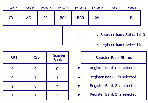
Fig 7 Program Status Word
The functions of above mentioned four flags are
CY (Carry Flag)
- When there is carry from D7 bit this flag is set.
- Usually, after arithmetic operations like addition and subtraction this flag is affected.
- With instructions like SET BC and CLRC this bit can be set to 1 or 0.
AC (Auxiliary Flag)
- This bit is set when a carry is generated from D3 to D4 during arithmetic operation. If not then it is clear.
- When instructions performing BCD arithmetic are executed this bit is used.
P (Parity Flag)
- The number of 1 in the accumulator are shown through this flag.
- When number of 1 in accumulator are 1, P=1 and P=0 when number of 1 in accumulator is even.
OV (Overflow Flag)
- When result of signed number operation is large this flag is set. Because of which higher order bit overflow into the sign bit.
- To detect error in signed arithmetic operations this flag is used.
Key takeaway
It is an 8-bit register out of which only 6-bits are used by 88051 Microcontroller. It has four flags which are affected as a result of some execution of any instruction. These flags are CY-carry, AC-auxiliary carry, P-Parity, OV-Overflow.
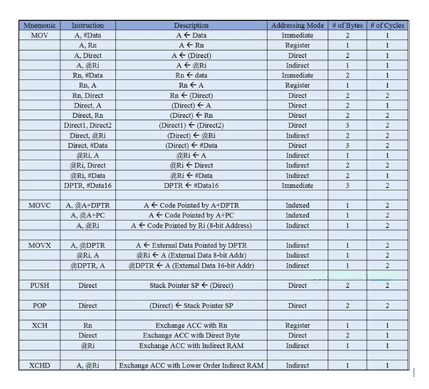
Data Transfer Instructions
The Data Transfer Instructions relate to transfer of data between registers or external program memory or data memory. The Mnemonics associated with Data Transfer are given below.
- MOV
- MOVC
- MOVX
- PUSH
- POP
- XCH
- XCHD
Arithmetic Instructions
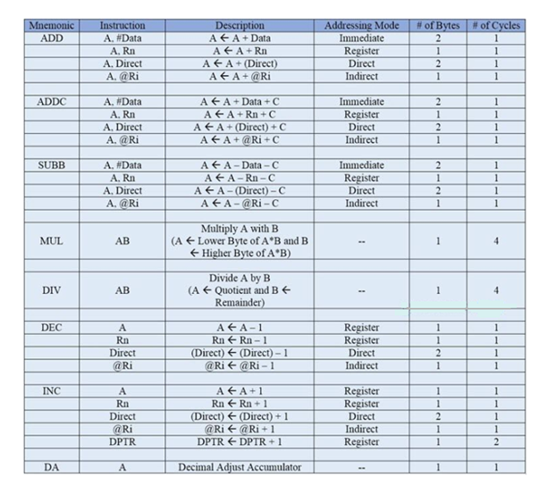
Using Arithmetic Instructions, one can perform addition, subtraction, multiplication and division. It consists of increment by one, decrement by one and a special instruction called Decimal Adjust Accumulator.
The Mnemonics associated with the Arithmetic Instructions of the 8051 Microcontroller Instruction Set are:
- ADD
- ADDC
- SUBB
- INC
- DEC
- MUL
- DIV
- DA A
The arithmetic instructions have no knowledge about the data format that is signed, unsigned, ASCII, BCD, and so on. The operations performed by the arithmetic instructions affect flags like carry, overflow, zero, etc. in PSW Register.
Logical Instructions
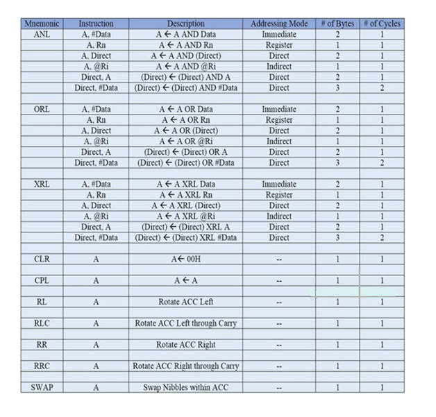
Logical Instructions perform logical operations like AND, OR, XOR, NOT, Rotate, Clear and Swap. Logical Instruction are performed on bytes of data on a bit-by-bit basis.
Mnemonics associated with Logical Instructions are as follows:
- ANL
- ORL
- XRL
- CLR
- CPL
- RL
- RLC
- RR
- RRC
- SWAP
Bit Manipulation Instructions
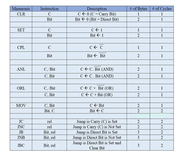
Boolean or Bit Manipulation Instructions will deal with bit variables. There is a special bit-addressable area in RAM and some Special Function Registers (SFRs) that are bit addressable.
The Mnemonics corresponding to the Boolean or Bit Manipulation instructions are:
- CLR
- SETB
- MOV
- JC
- JNC
- JB
- JNB
- JBC
- ANL
- ORL
- CPL
These instructions perform set, clear, and, or, complement at bit level. All the possible mnemonics of the Boolean Instructions are specified in the following table.
Program Branching Instructions
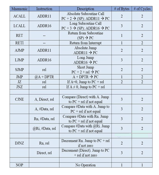
The logic of the program is controlled by these instructions. The mnemonics of the Program Branching Instructions are:
- LJMP
- AJMP
- SJMP
- JZ
- JNZ
- CJNE
- DJNZ
- NOP
- LCALL
- ACALL
- RET
- RETI
- JMP
All these instructions, except the NOP (No Operation) affect the Program Counter (PC) Some of these instructions have decision making capability before transferring control to other part of the program.
The following table shows all the mnemonics with respect to the program branching instructions.
Key takeaway
There are following group of instructions:
- Arithmetic Instructions.
- Data transfer Instructions.
- Bit Manipulation.
- Program Branching Instructions.
- Logical Instructions.
Exchange the content of FFH and FF00H
MOV dptr, #0FF00H ; take the address in dptr
MOVX A, @dptr ; get the content of 0050H in a
MOV r0, 0FFH ; save the content of 50H in r0
MOV 0FFH, a ; move a to 50H
MOV A, r0 ; get content of 50H in a
MOVX @dptr, a ; move it to 0050H
Store the higher nibble of r7 in to both nibbles of r6
Firstly, we get the upper nibble of r7 in r6. Then we swap nibbles of r7 and make OR operation with r6 so the upper and lower nibbles are duplicated
MOV A, r7 ; get the content in acc
ANI A, #0F0h ; mask lower bit
MOV r6, A ; send it to r6
SWAP A ; xchange upper and lower nibbles of accumulator
ORL A, r6 ; OR operation
MOV r6, A ; finally load content in r6
Transfer the block of data from 20H to 30H to external location 1020H to 1030H.
MOV r7, #0AH ; initialize counter by 10d
MOV r0, #20H ; get initial source location
Mov dptr, #1020H ; get initial destination location
Nxt: MOV A, @r0 ; get first content in acc
MOVX @dptr, a ; move it to external location
INC r0 ; increment source location
INC dptr ; increase destination location
DJNZ r7, nxt ; decrease r7. If zero then over otherwise move next
Given block of 100h to 200h. Find out how many bytes from this block are greater then, the number in r2 and less then number in r3. Store the count in r4.
MOV dptr, #0100H ; get initial location
MOV r7, #0FFH ; counter
MOV r4, #00H ; number counter
MOV 20H, R2 ; get the upper and lower limits in
MOV 21H, R3 ; 20H and 21H
Nxt: MOVX A, @dptr ; get the content in acc
CJNE A, 21H, lower ; check the upper limit first
SJMP out ; if number is larger
Lower: JNC out ; jump out
CJNE A, 20H, limit ; check lower limit
SJMP out ; if number is lower
Limit: JC out ; jump out
INC r4 ; if number within limit increment count
Out: INC dptr ; get next location
DJNZ r7, nxt ; repeat until block completes
Find out how many equal bytes between two memory blocks 10H to 20H and 20H to 30H.
MOV r7, #0AH ; initialize counter by 10d
MOV r0, #10H ; get initial location of block1
MOV r1, #20H ; get initial location of block2
MOV r6, #00H ; equal byte counter. Starts from zero
Nxt: MOV A, @r0 ; get content of block 1 in acc
MOV b, a ; move it to B
MOV A, @r1 ; get content of block 2 in acc
CJNE A, B, nomatch ; compare both if equal
INC r6 ; increment the counter
Nomatch: INC r0 ; otherwise go for second number
INC r1
DJNZ r7, nxt ; decrease r7. If zero then over otherwise move next
A stack is a last in first out memory. In 8051 internal RAM space can be used as stack. The address of the stack is contained in a register called stack pointer. Instructions PUSH and POP are used for stack operations. When a data is to be placed on the stack, the stack pointer increments before storing the data on the stack so that the stack grows up as data is stored (pre-increment). As the data is retrieved from the stack the byte is read from the stack, and then SP decrements to point the next available byte of stored data (post decrement). The stack pointer is set to 07 when the 8051 resets. So that default stack memory starts from address location 08 onwards (to avoid overwriting the default register bank ie., bank 0). Eg; Show the stack and SP for the following.
[SP]=07 //CONTENT OF SP IS 07 (DEFAULT VALUE)
MOV R6, #25H [R6]=25H //CONTENT OF R6 IS 25H
MOV R1, #12H [R1]=12H //CONTENT OF R1 IS 12H
MOV R4, #0F3H [R4]=F3H //CONTENT OF R4 IS F3H
PUSH 6 [SP]=08 [08]=[06]=25H //CONTENT OF 08 IS 25H
PUSH 1 [SP]=09 [09]=[01]=12H //CONTENT OF 09 IS 12H
PUSH 4 [SP]=0A [0A]=[04]=F3H //CONTENT OF 0A IS F3H
POP 6 [06]=[0A]=F3H [SP]=09 //CONTENT OF 06 IS F3H
POP 1 [01]=[09]=12H [SP]=08 //CONTENT OF 01 IS 12H
POP 4 [04]=[08]=25H [SP]=07 //CONTENT OF 04 IS 25H
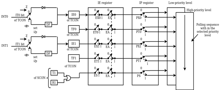
Figure 8. Interrupt Structure of 8051.
8051 has five interrupts. These are INT0, INT1, T0, T1, TI/RI. All these interrupts can be enabled or disabled by IE (interrupt enable) register.
Interrupt Enable (IE)Register
This register can be used to enable or disable interrupts by programming. It is an SFR with address A8H. This byte is bit addressable hence can be programmed by the user. Every bit in this register has a specific meaning.


Interrupt Priority (IP) Register
The five interrupts can be either one or two interrupt level. The priority levels are level 1 and level 0. Higher Priority is indicated by level 1 and level 0 indicates lower priority. To store priority levels for each interrupt IP register is used. This is bit addressable SFR with address B8H.


External Interrupt
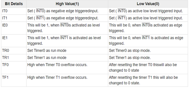
The external interrupts are INT0 and INT1. The TCON register can be used to program external interrupts to edge or level triggered. The TCON is Timer Control. TCON is another bit addressable SFR. The address is 88H.
Key takeaway
Interrupt is a subroutine call that interrupts the microcontroller's main operations or work and causes it to execute any other program, at the time of operation. It provides a mechanism to put on hold the ongoing operations, execute a subroutine and resume to another type of operation.
8051 has five interrupts as mentioned below:
- INTO
- TFO
- INT1
- TF1
- R1/T1
The interrupts (INT0) ̅ and (INT1) ̅ are called as external interrupts. The interrupts (INT0) ̅ and (INT1) ̅ are negative edge triggered. When, these interrupts are activated, the corresponding flags are set except for serial interrupts.
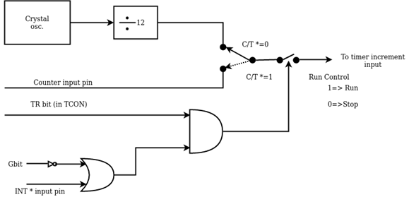
There are two 16-bit timer registers are known as Timer0 and Timer1. The timer registers are used as Timer mode and Counter mode. The only difference in these two modes is the source for incrementing the timer registers.
Timer Mode
In timer mode, it counts internal machine cycles. So, this register gets incremented for each machine cycle. When the clock frequency is 12MHz, timer register is incremented for every millisecond. It ignores external timer input pin in this mode.
Counter Mode
In counter mode, it counts external events. The timer register gets incremented for every 1 to 0 transition in the external input pin. This type of transitions is referred as events.
The external input pins are sampled once for each machine cycle. In order to determine 1or 0 transitions another machine cycle is required.
Therefore, atleast two machine cycles are required in this mode. When frequency is12MHz the maximum count frequency will be 12MHz/24 = 500KHz. So, for event counting time duration is 2 µs.
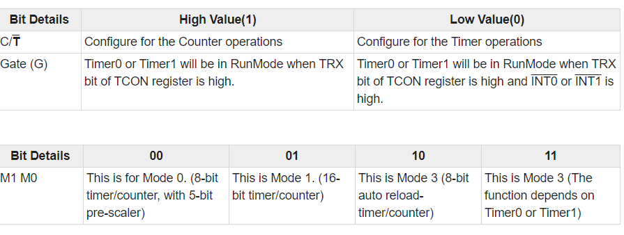
Timer or Counter has four different modes. Mode 0 to Mode 2 are for both Timer/Counter. Mode 3 represent different meaning for each timer register. There is a register called TMOD which can be programmed to configure these timers or counters.
The Serial port is used for serial communication in mode 1 and 3. For baud rate generation timer1 is used. Hence, Timer0 is available for timer or counter operations.
TMOD Register
TMOD(Timer Mode) is an SFR. The address of this register is 89H. This is not bit-addressable.

Mode 0 of Timer/Counter
Mode 0 operation is 8-bit timer or counter with 5-bit pre-scaler. It is 13-bit timer/counter. Which uses 5 bits of TL0 or TL1 and 8-bits of TH0 or TH1.

Figure 9. Mode 0
Mode 1 of Timer/Counter
Mode 1 operation is 16-bit timer or counter. In the following diagram, Mode 1 is used for Timer0.

Figure 10. Mode 1
Mode 2 of Timer/Counter
Mode 2 operation is 8-bit auto reload timer or counter. Mode 2 is used for Timer1.
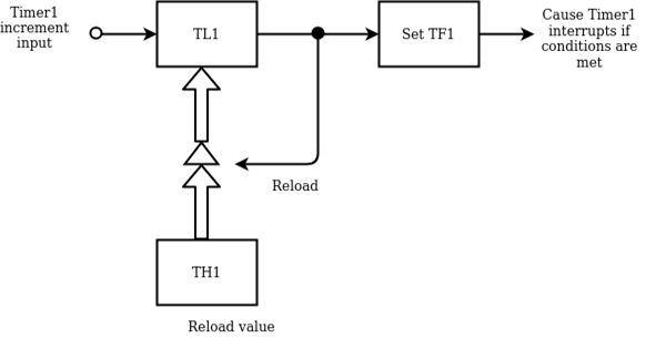
Figure 11. Mode 2
Mode 3 of Timer/Counter
Mode 3 is different for Timer0 and Timer1. When Timer0 is working in mode 3, TL0 will be used as 8-bit timer/counter. It will be controlled by standard Timer0 control bits, T0 and INT0 inputs. TH0 is used as 8-bit timer not counter. This is controlled by Timer1 Control bit TR1. When the TH0 overflows from FFH to 00H, TF1 is set to 1. In the following diagram, Timer0 is in Mode 3.

Figure 12. Mode 3
Operation:
- It controls the running of 8-bit timer/counter TL0 like Mode 0, 1, or 2. The running of TH0 is controlled by TR1 bit. So, the gate bit in this mode for Timer0 has no specific role.
- The mode 3 is present for applications requiring an extra 8-bit timer/counter. In Mode 3 of Timer0, 8051 has three timers. One 8-bit timer by TH0, another8-bit timer/counter by TL0, and one 16-bit timer/counter by Timer1.
- If Timer0 is in mode3, and Timer1 is working on either 0, 1 or 2, then the gun control of the Timer1 is activated when the gate bit is low or INT1 is high. The run control is deactivated when the gate is high and INT1 is low.
Key takeaway
Timer or Counter has four different modes. Mode 0 to Mode 2 is for both Timer/Counter. Mode 3 represent different meaning for each timer register. There is a register called TMOD which can be programmed to configure these timers or counters.
The Serial port is used for serial communication in mode 1 and 3. For baud rate generation timer1 is used. Hence, Timer0 is available for timer or counter operations.
It is also called the Universal Asynchronous Receiver Transmitter used in serial communication. It basically does serial to parallel data conversion on the transmitter side. Again, at the receiver side it converts the received data from serial to parallel. It is an interconnection between the processor and the serial communication port.

Figure 13. UART
Above figure shows the connection of UART with the controller and USB interface. The timing settings between the transmitter and receiver in this case are of major concern. To maintain synchronisation UART uses special bits at the starting and end of each word.
The UART at the sender end receives the parallel data and converts it to serial data. The receiving side UART receives this serial data and converts it to parallel and sends it back to the CPU.
Working of UART
The transmission in UART is asynchronous. The transmitter and receiver do not have any timing synchronisation. There are special bits which are used for synchronisation. They are called Start and Stop bits.
These bits are attached at the start and end of the data allowing the receiver to identify the actual data. The data bus transfers the data to the transmitting UART from the controlling device. This received data is in parallel.
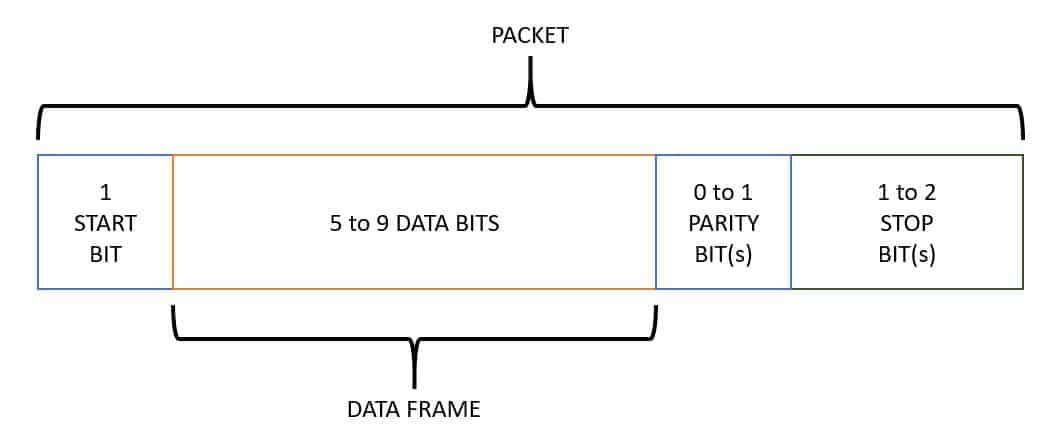
The start, parity and stop bits are added to this received data. After inserting the special bits they are converted to serial data with the help of shift registers. At the Rx pin the receiving UART receives this serial data. The original data is recognised by the special bits. Parity bit is used to check the integrity of the data.
The special bits are separated from the received data and it is again converted back to parallel data. Through the data bus this data is sent back to the receiving end of the controller.
Necessary requirement for UART
The requirements for data transmission are mentioned below.
- Synchronisation Bits (Start and Stop bits)
- Parity Bit
- Data Bits and
- Baud Rate
The rate of data transmission is called Baud rate. It is measured in bits per second.
Calculation of Baud Rate
In order to calculate the machine cycle frequency, the 8051 divides the crystal frequency by 12. The oscillator frequency is 11.0592 MHz.

Figure 14. Oscillator Frequency
Here the oscillator is XTAL = 11.0592 MHz, the machine cycle frequency is 921.6 kHz. 8051's UART divides the machine cycle frequency of 921.6 kHz by 32 once more before it is used by Timer 1 to set the baud rate. 921.6 kHz divided by 32 gives 28,800 Hz. Timer 1 must be programmed in mode 2, that is 8-bit, auto-reload.
Example
In serial communication if data transferred with a baud rate of 9600 and XTAL used is 11.0592 then following is the steps followed to find the TH1 value to be loaded.
Clock frequency of timer clock: f = (11.0592 MHz / 12)/32 = 28,800Hz
Time period of each clock tick: T0 = 1/f = 1/28800
Duration of timer: n*T0 (n is the number of clock ticks)
9600 baud ->duration of 1 symbol: 1/9600
1/9600 = n*T0 = n*1/28800
n = f/9600 = 28800/9600 = 3 ->TH1 =-3
Similarly, for baud 2400 n = f/2400 = 12 ->TH1 = -12
Registers are known as data storage devices. There are two registers namely Register A and Register B. Register A is used as an accumulator and Register B as general -purpose register. The output of mathematical and logical instructions are stored in these registers.
The operations of addition, subtraction, multiplication and division are performed by Register A. Register B is for multiplication and division which are carried by Register A. For data transfers between microcontroller and external memory Register A is involved.
8051 microcontrollers also has 7 Special Function Registers (SFRs). They are:
1. Serial Port Data Buffer (SBUF)
2. Timer/Counter Control (TCON)
3. Timer/Counter Mode Control (TMOD)
4. Serial Port Control (SCON)
5. Power Control (PCON)
6. Interrupt Priority (IP)
7. Interrupt Enable Control (IE)
Timers and Counters
In internal operations synchronization is achieved by clock circuits for generating clock pulses. During each clock pulse operations assure synchronization.
For oscillator formation XTAL1 and XTAL2 are used to form resonant network. It consists of four more pins.
1. EA: External enable
2. ALE: Address latch enable
3. PSEN: Program store enable and
4. RST: Reset.
Quartz crystal is used for generating periodic clock pulses.
Internal RAM and ROM
ROM
In 8051 a code of 4K memory is incorporated as on-chip ROM. ROM is a non-volatile memory that is its contents cannot be altered. They can address program memory and data memory which is a separate block of 64KB.
RAM
The internal RAM of 8051 microcontroller is composed of 128 bytes. It is a volatile memory because its contents is lost if power is switched off.
In internal RAM 128 bytes is divided into 32 working registers which constitute of 4 register banks (Bank 0-Bank 3) , each bank consisting of 8 registers (R0 - R7). Internal RAM consists of 128 addressable bits.
Four General Purpose Parallel Input/Output Ports
It consists of four 8-bit input/output ports. These are:
PORT P0: In absence of external memory present, this port acts as a general-purpose input/output port. In the presence of external memory, it operates as multiplexed address and data bus performing dual role.
PORT P1: This port is used for different interfacing activities. This 8-bit port is a normal I/O port and does not perform dual functions.
PORT P2: Port 2 is like PORT P0 which is used as general- purpose port if no external memory is present. However, in presence of external memory, it works in conjunction with PORT PO as an address bus. This is an 8-bit port which performs dual functions.
PORT P3: PORT P3 behaves as dedicated I/O port
Interrupt Control
An interrupt is either an internal or external event where the microcontroller suspends for a certain time by obstructing the sequential flow of a program.
There are two ways of giving interrupts to a microcontroller
– Sending software instructions
- Sending hardware signals.
In interrupt mechanism 8051 keeps the normal program execution in “put on hold" mode and executes a subroutine program. After execution of subroutine it returns to normal program execution. This subroutine program is called an interrupt handler. A subroutine is executed when certain event occurs.
8051 is provided with 5 sources of interrupts are provided.
They are:
a) Two external interrupt sources connected through INT0 and INT1
b) Three external interrupt sources- serial port interrupt, Timer Flag 0 and Timer Flag 1.
Serial Data Communication
In serial data communication is established among computers by transmitting and receiving data bits in a serial connection network.
For holding data SBUF (Serial Port Data Buffer) register;
Manage data communication SCON (Serial Control) register
Managing data transfer rate PCON (Power Control) register
RXD and TXD establish serial network.
SBUF register has 2 parts
For storing the data to be transmitted use TXD pin
For receiving data from other source use RXD pin.
Serial data communication operate in four modes. They are serial data
1. Mode 0 (shift register mode)
2. Mode 1 (standard UART)
3. Mode 2 (multiprocessor mode)
4. Mode 3
PSW (Program Status Word)
Program Status Word or PSW is a hardware register a memory location which holds a program's information and monitors the status of the program this is currently being executed. It has a pointer which points towards the address of the next instruction to be executed.
The register has 3 fields namely instruction address field, condition code field and error status field. PSW is an internal register which keeps track of the computer at every instant.
There are7 flags in PSW. 4 are math flags and 3 are general purpose or user flags.
The Math flags are:
• Carry (c)
• Auxiliary carry (AC)
• Overflow (OV)
• Parity (P)
The General purpose flags or User flags are:
• FO
• GFO
• GF 1
Data Pointer (DPTR)
DPTR is a 16-bit register. It consists of two 8-bit registers DPH and DPL. Separate addresses are assigned to each DPH and DPL. These 8-bit registers are used for storing memory addresses which can be accessed internal and external data/code.
Stack Pointer (SP)
A special area of data in memory. The stack pointer is an 8-bit register whose main function is to access the stack. It can take values in the range 00 H to FF H. SP acts as a pointer to points to an address at the top of the stack.
Data and Address Bus
A bus consists of group of wires to transfer data from one location to another within the system. Buses reduce the number of paths or cables needed to set up connection between components.
There are two kinds of buses:
Data Bus and Address Bus
Data Bus: The purpose of data bus is to transfer data. It acts as a channel for data to travel.
Address Bus: The purpose of address bus is to transfer information but not data. The information tells from where within the components, the data should be sent to or received from.
Five ports are selected depending on the device and features selected.When a peripheral is enabled the pin is not used as general purpose I/O pin.
Each port has three registers for its operation:
- TRIS registers (Data Direction register)
- PORT register (reads the levels on the pins of the device)
- LAT register (Data Latch register)
The data latch is used for read-modify write operations depending on the value of I/O pins.
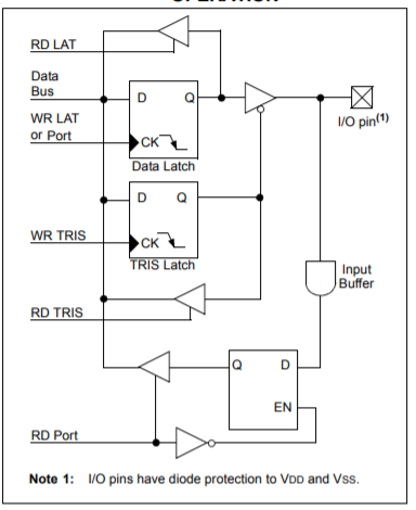
Figure 15. Port Operation
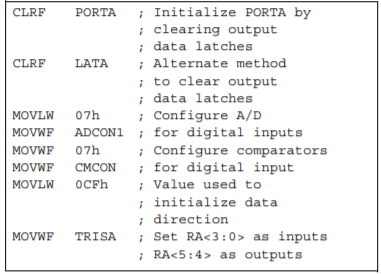
The TRISA register controls PORTA pins direction while being used as analog inputs. The user must ensure that the bits in TRISA register are set when using them as analog inputs.
Program for initializing port A
PORTB is an 8-bit wide, bidirectional port. The Data Direction register is TRISB. When TRISB bit (= 1) then PORTB pin serves as input. Clearing a TRISB bit (= 0) PORTB pin serves as output. The Data Latch register (LATB) is memory mapped. Read-modify-write operations on LATB register read and write the latched output value for PORTB.

Program for initializing Port B
PORTC is an 8-bit wide, bidirectional port. The Data Direction register is TRISC. Setting a TRISC bit (= 1) will make PORTC pin an input. Clearing a TRISC bit (= 0) will make the PORT C pin an output. The Data Latch register (LATC) is memory mapped. Read-modify-write operations on LATC register read and write the latched output value for PORTC. When enabling peripheral functions, define TRIS bits for each PORTC pin. Some peripherals override TRIS bit to make the pin an output, while other peripherals override the TRIS bit to make the pin as input.
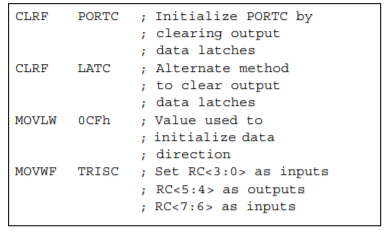
Program for initializing Port C
PORTD is an 8-bit wide, bidirectional port. The corresponding Data Direction register is TRISD. Setting a TRISD bit (= 1) will make the corresponding PORTD pin an input. Clearing a TRISD bit (= 0) will make the corresponding PORTD pin an output. The Data Latch register (LATD) is also memory mapped. Read-modify-write operations on the LATD register read and write the latched output value for PORTD.
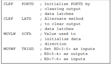
Program for initializing Port D
The fourth pin of PORTE (MCLR/VPP/RE3) is an input pin. Its operation is controlled by MCLRE configuration bit. When selected as port pin (MCLRE = 0), it functions as digital input pin; Otherwise, it functions as the device’s Master Clear input. In either configuration, RE3 functions as programming voltage input during programming.
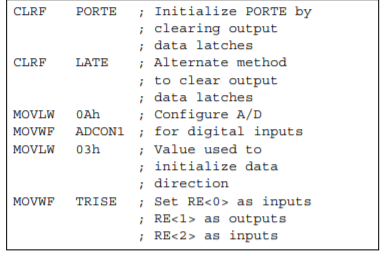
Program for initializing Port E
References:
1. The 8051 Microcontroller: A System Approach by Muhammad Mazidi, 1st Ed., PHI, 2012
2. D. M Calcutt, Fredrick J. Cowan " 8051 microcontroller: an application based introduction".
3. Subrata Ghoshal "8051 microcontroller" Pearson Education